
A Low-Power Analog Processor-in-Memory-Based Convolutional Neural Network for Biosensor Applications

 ,
,  ,
, 
Abstract
:1. Introduction
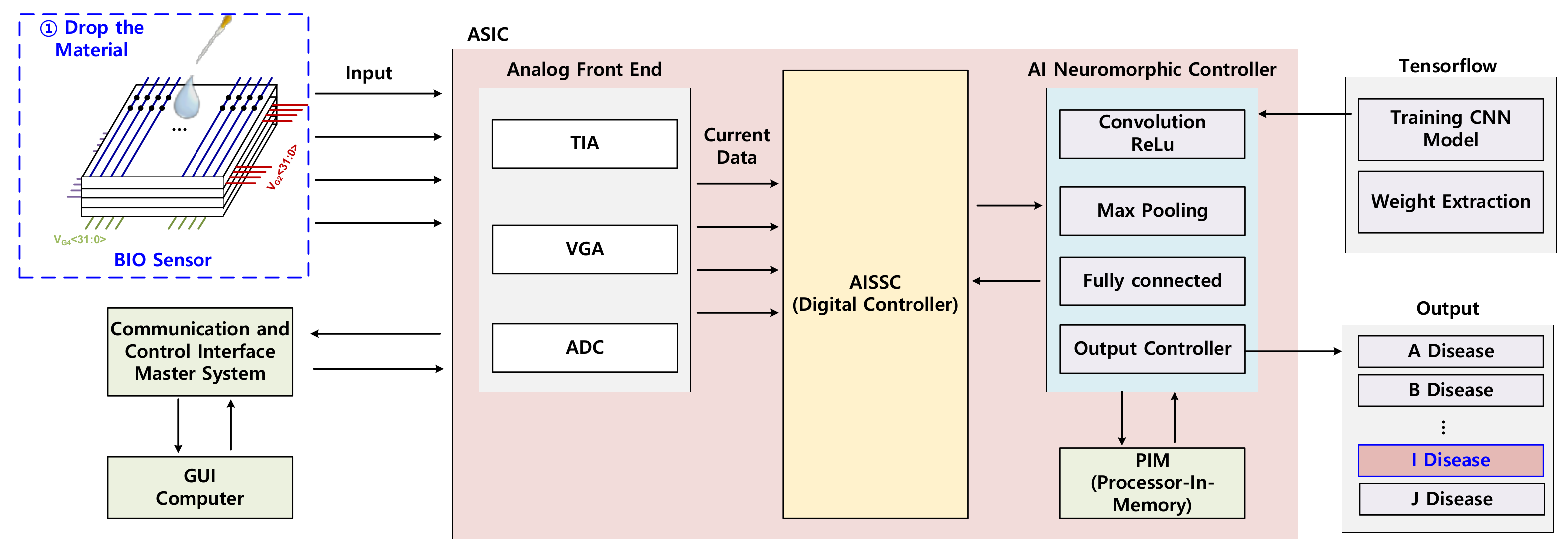
2. Architecture
2.1. Top Architecutre
2.2. Detailed Structure
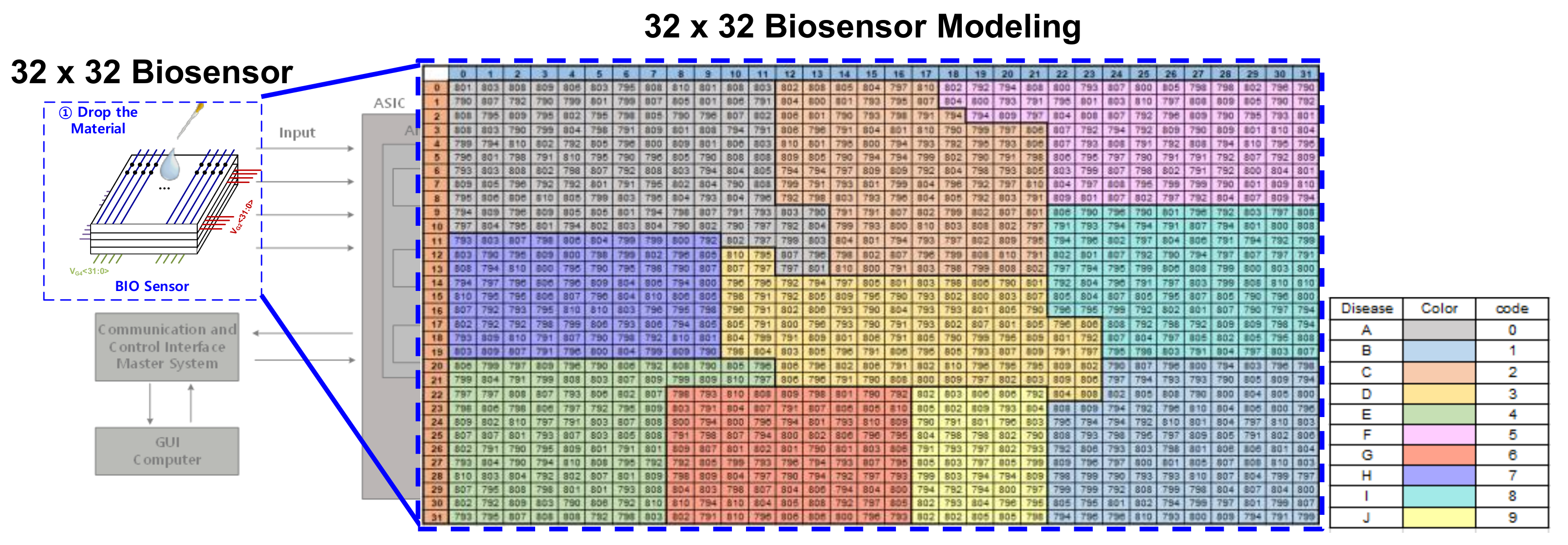
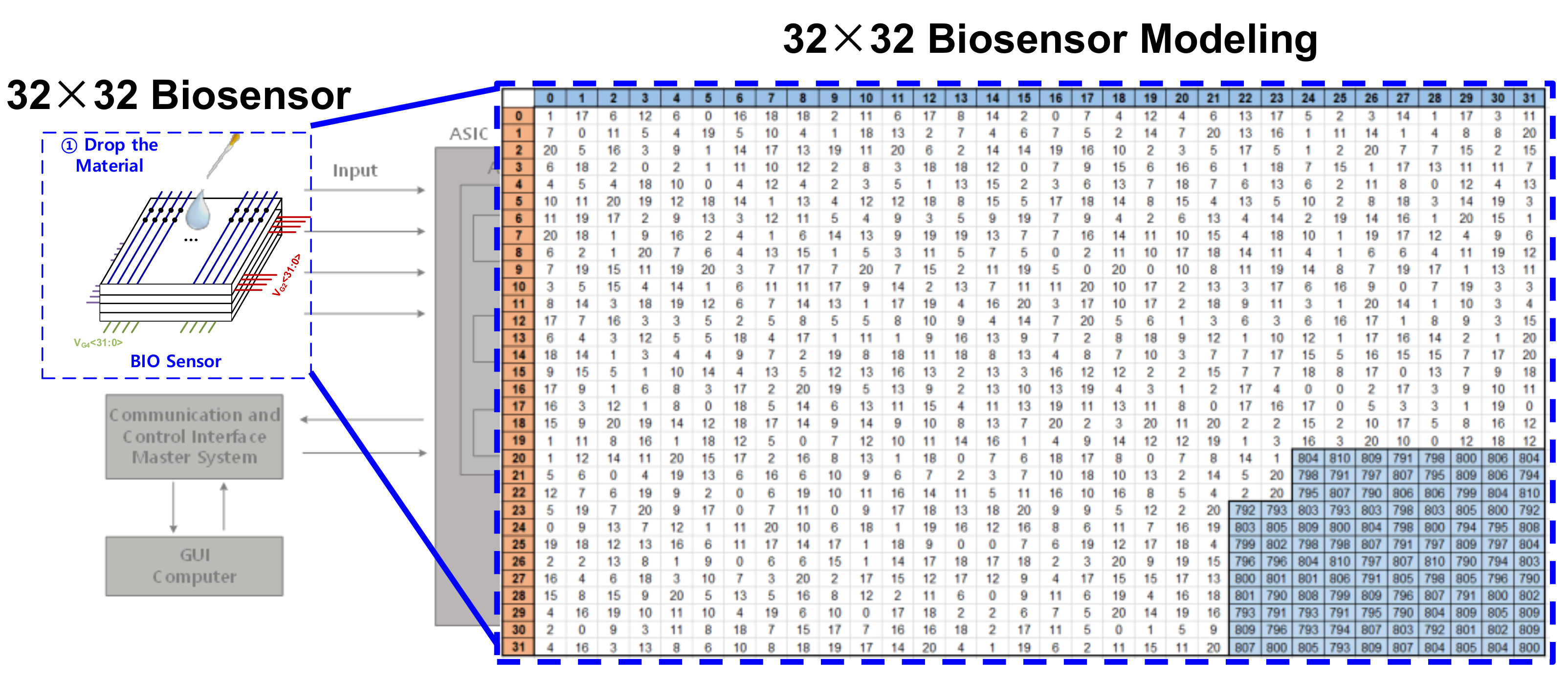
2.2.1. Input Feature
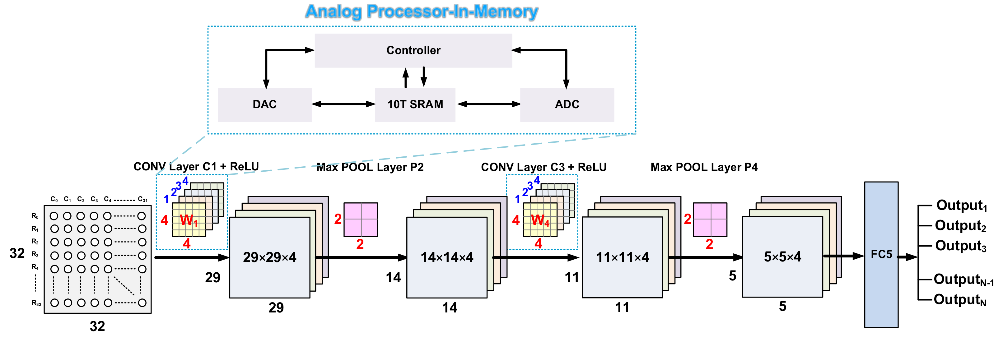
2.2.2. The Proposed CNN Model Architecture
2.2.3. The Proposed Analog CNN Filter
3. Experimental Results
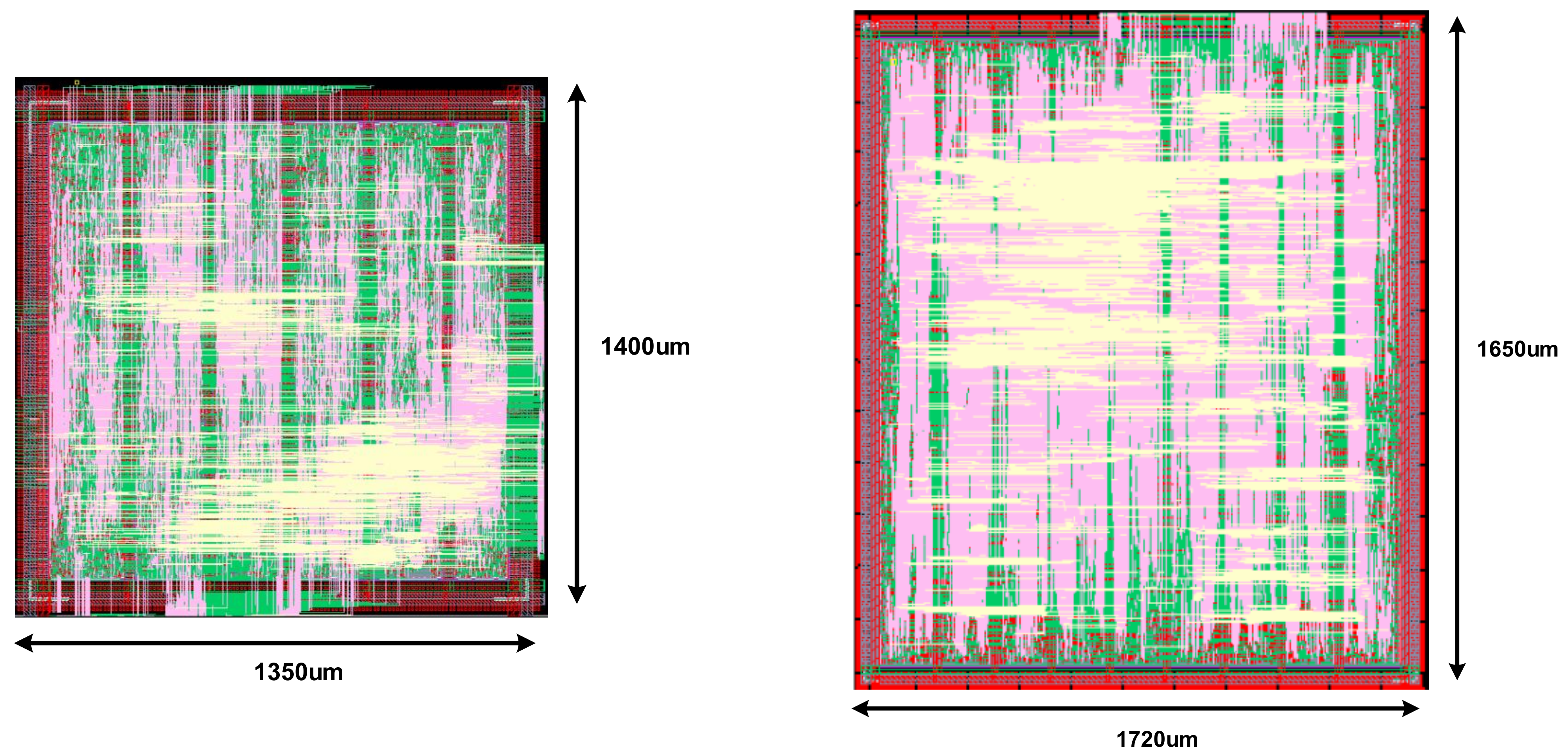
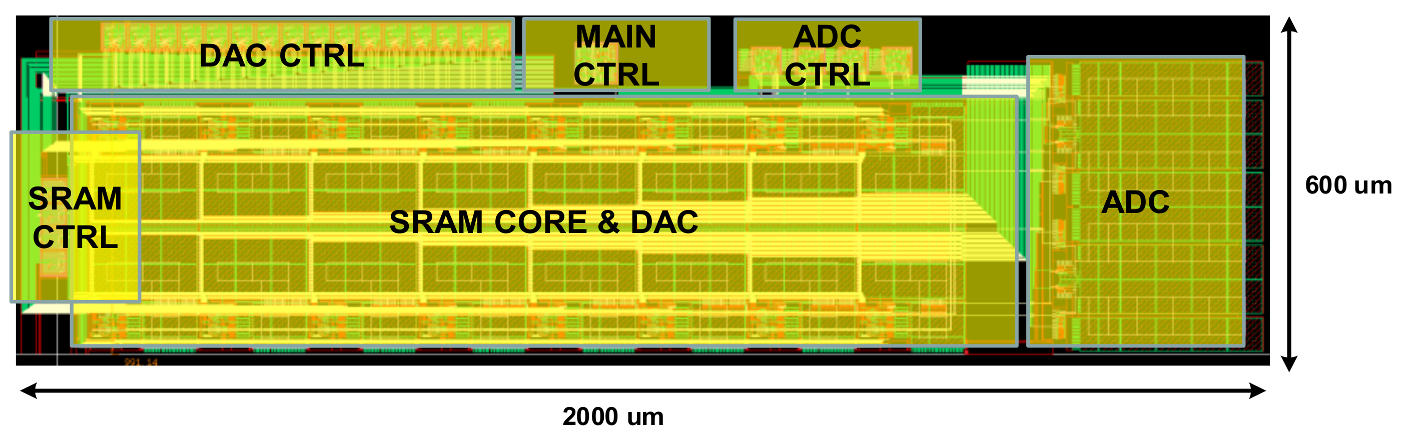
3.1. Implementation
3.2. Classification
3.3. CNN
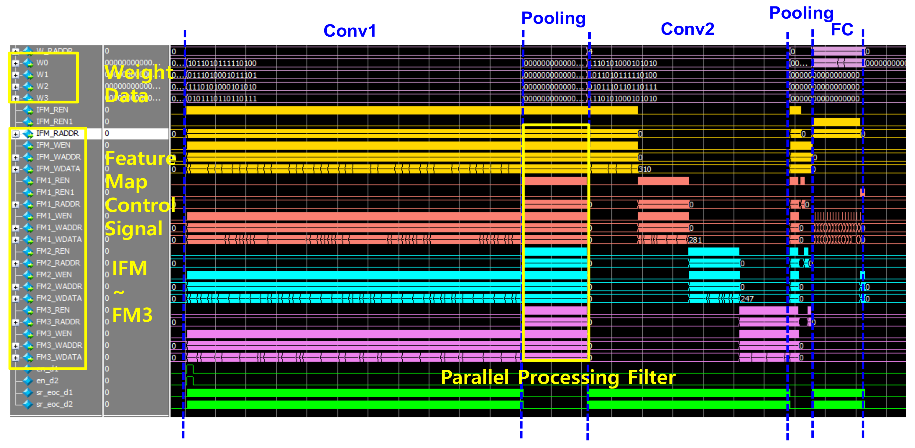
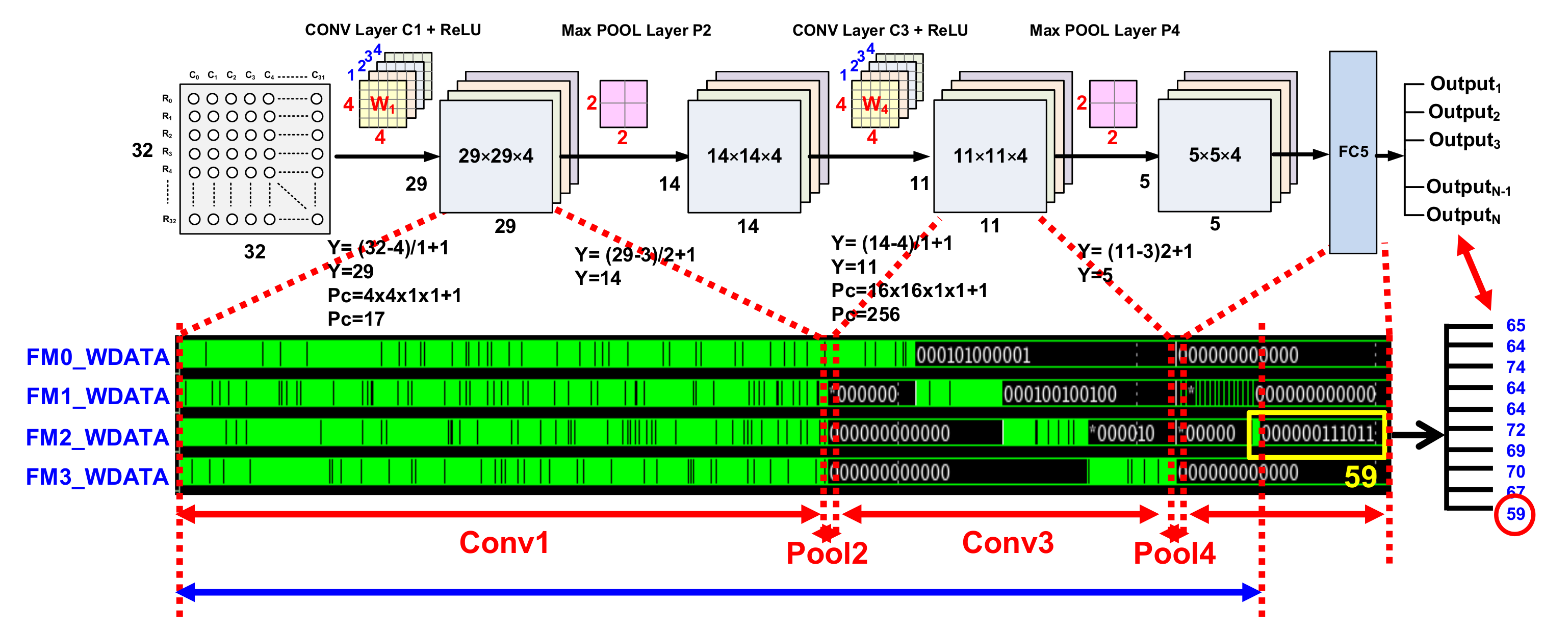
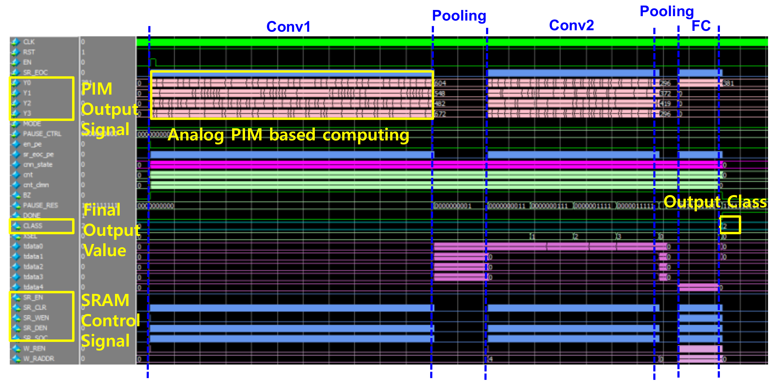
3.3.1. CNN Simulation
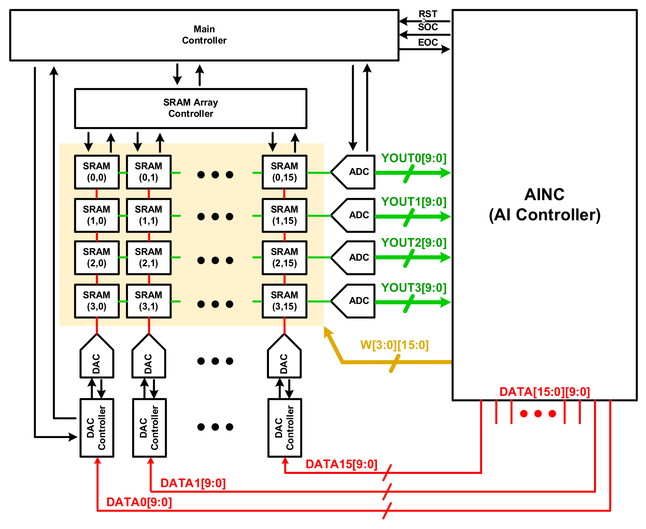
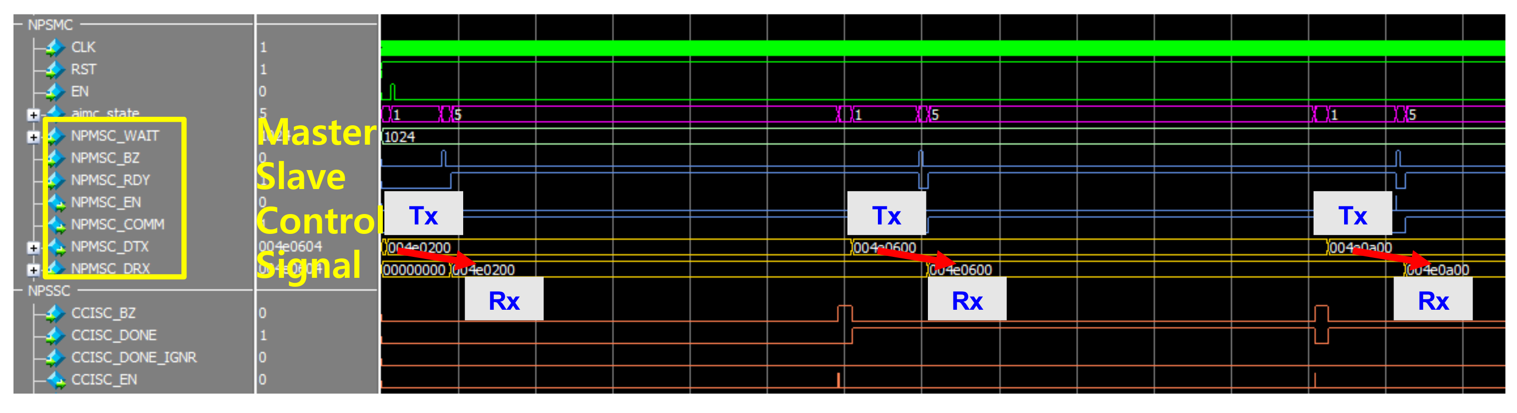
3.3.2. AI Main Controller (AIMC)
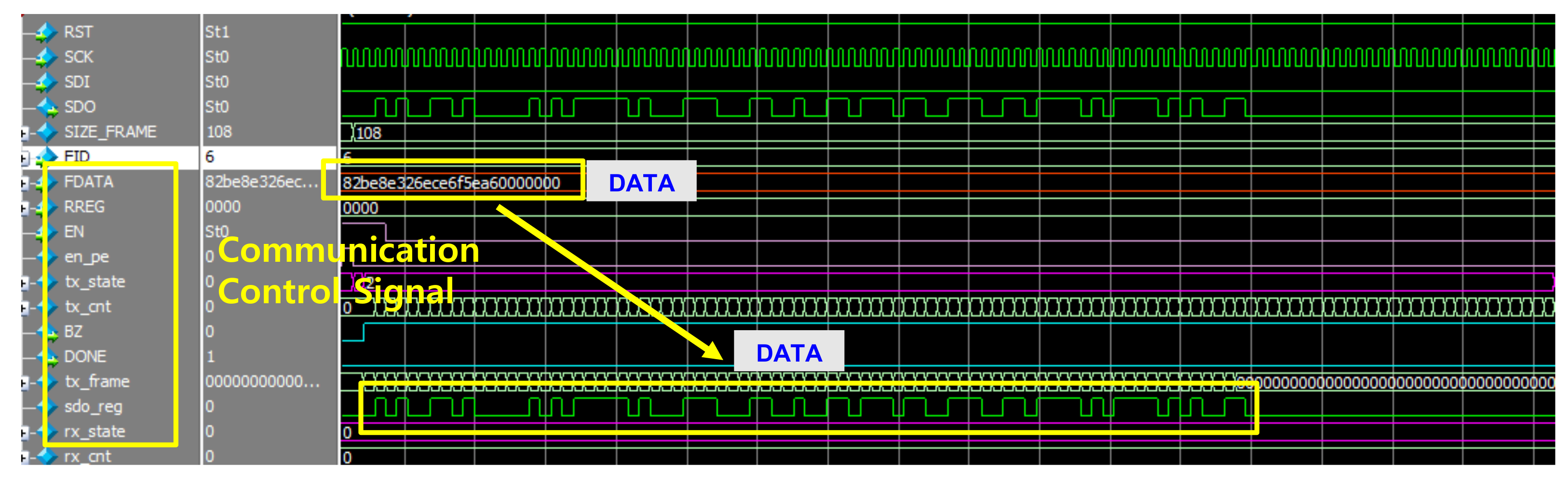
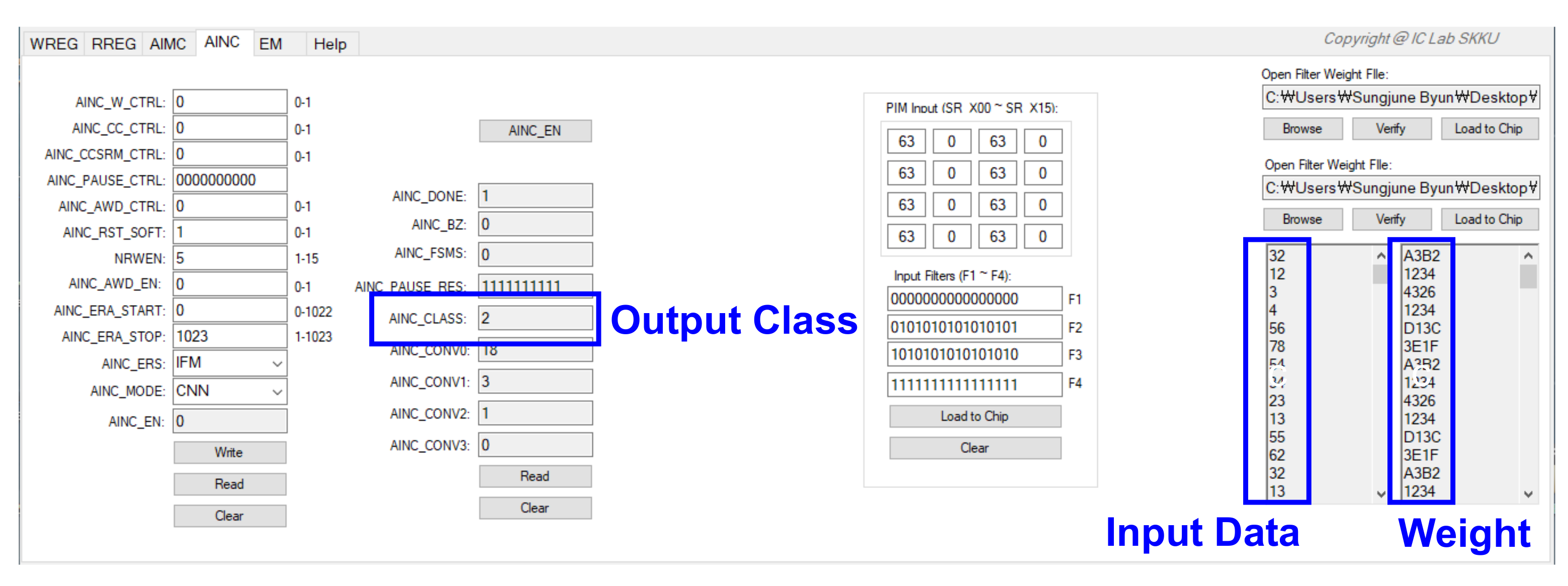
3.3.3. Communication and Control Interface
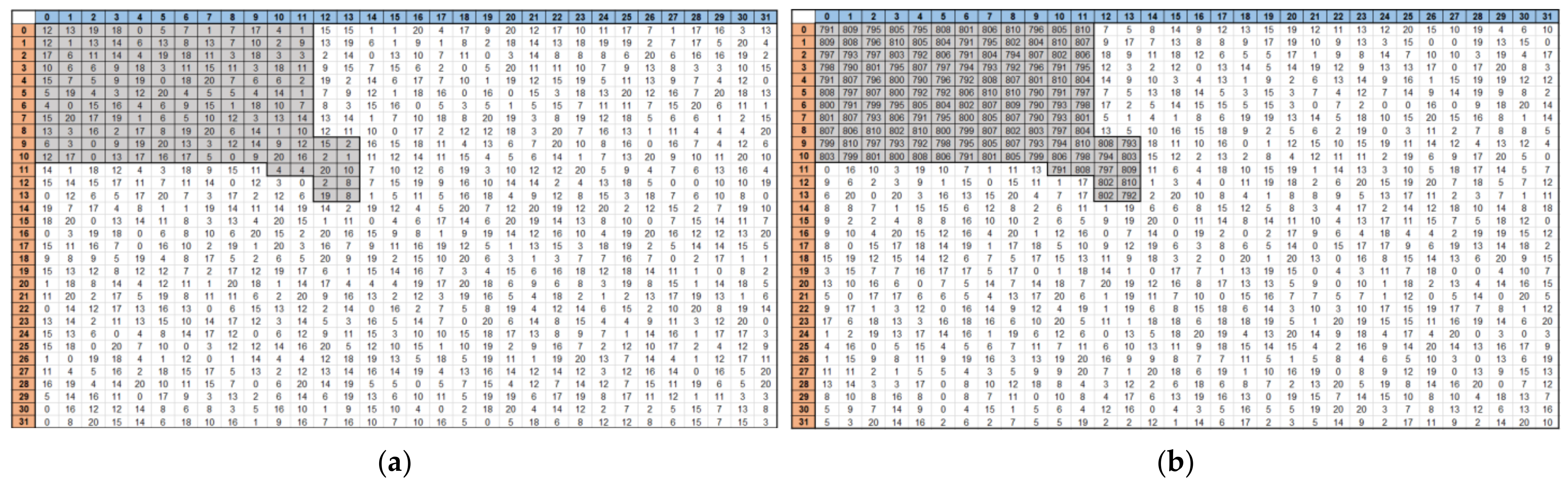
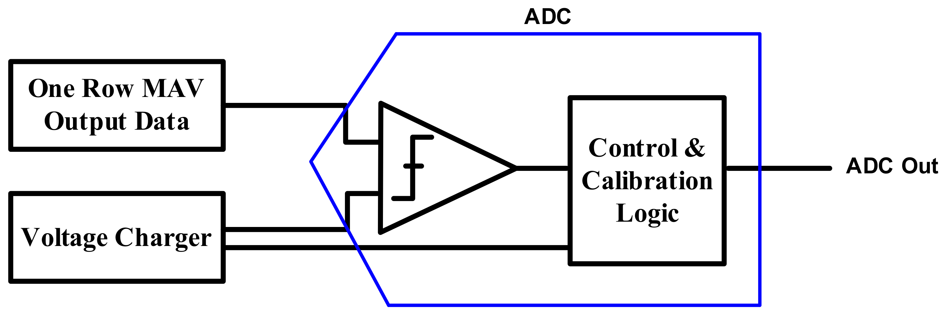
3.4. Processor-in-Memory
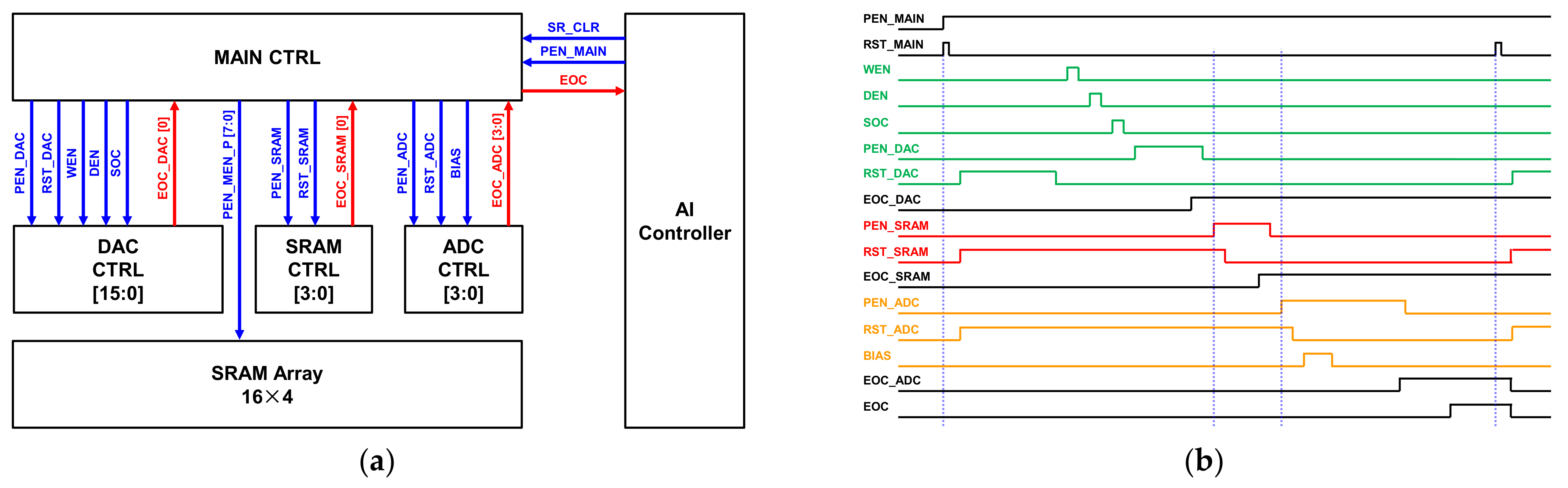
3.4.1. PIM Controllers
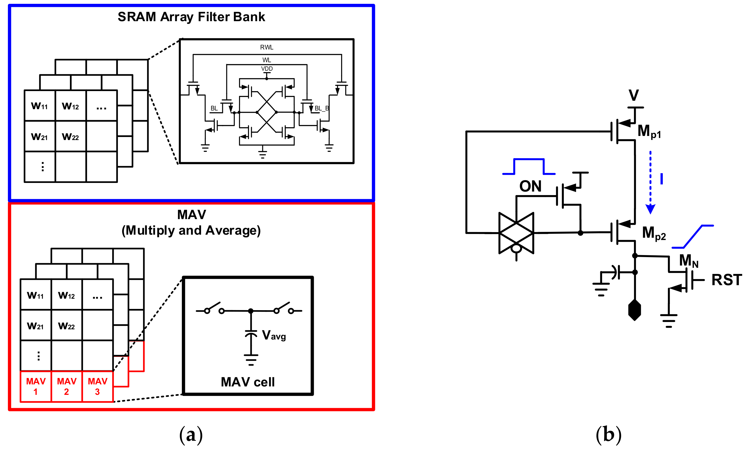
3.4.2. PIM Core
3.5. Measurement Result
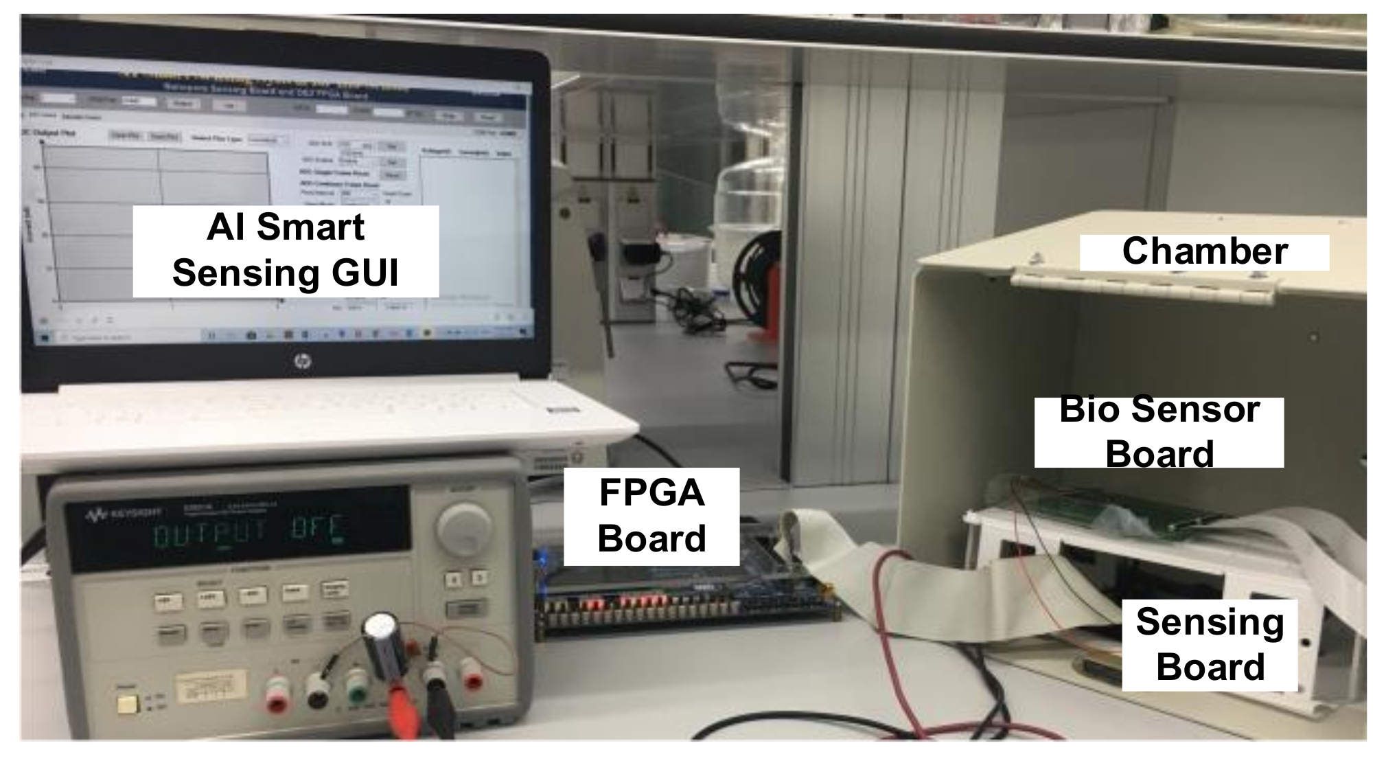
3.5.1. Measurement Environment
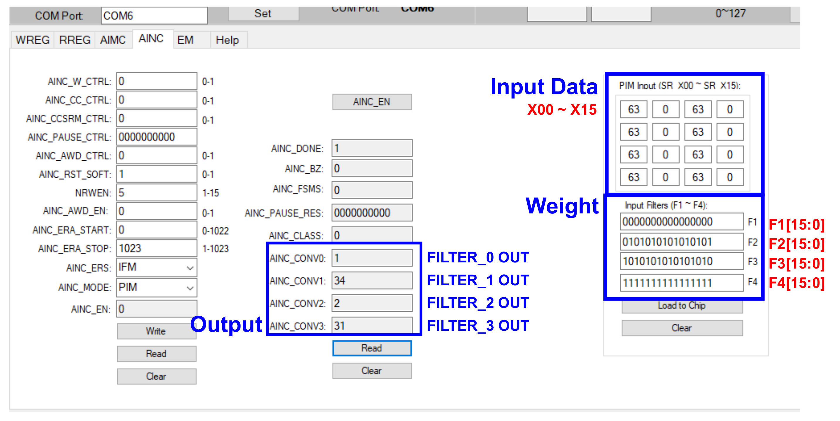
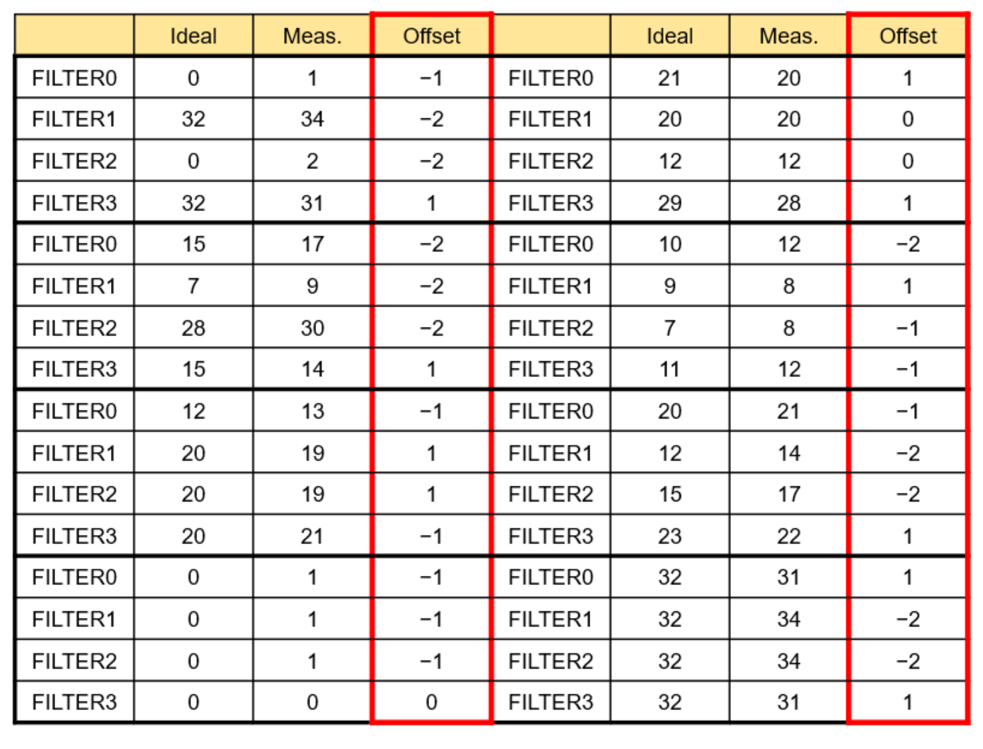
3.5.2. CNN Classification
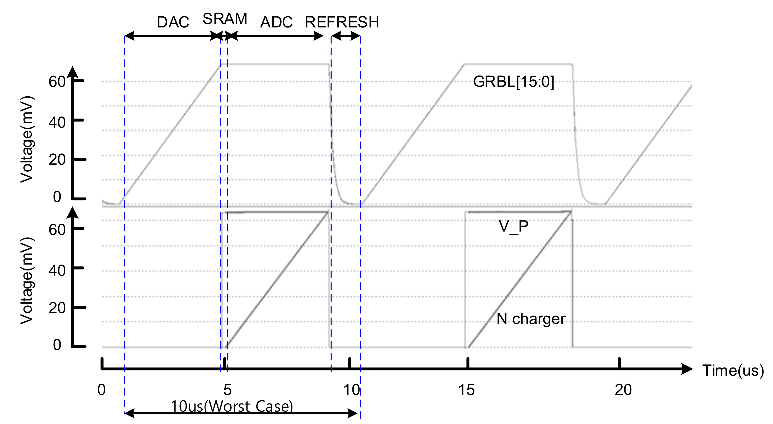
3.5.3. Processor-in-Memory
4. Conclusions
Funding
Institutional Review Board Statement
Informed Consent Statement
Acknowledgments
Conflicts of Interest
References
- LeCun, Y.; Bottou, L.; Bengio, Y.; Haffner, P. Gradient-based learning applied to document recognition. Proc. IEEE 1998, 86, 2278–2324. [Google Scholar] [CrossRef] [Green Version]
- LeCun, Y.; Boser, B.; Denker, J.S.; Henderson, D.; Howard, R.E.; Hubbard, W.; Jackel, L.D. Backpropagation applied to handwritten zip code recognition. Neural Comput. 1989, 1, 541–551. [Google Scholar] [CrossRef]
- Taigman, Y.; Yang, M.; Ranzato, M.; Wolf, L. Deepface: Closing the gap to human-level performance in face verification. In Proceedings of the IEEE Conference on Computer Vision and Pattern Recognition, Columbus, OH, USA, 23–28 June 2014; pp. 1701–1708. [Google Scholar]
- Kalchbrenner, N.; Grefenstette, E.; Blunsom, P. A convolutional neural network for modelling sentences. arXiv 2014, arXiv:1404.2188. [Google Scholar]
- Yadav, S.S.; Jadhav, S.M. Deep convolutional neural network based medical image classification for disease diagnosis. J. Big Data 2019, 6, 113. [Google Scholar] [CrossRef] [Green Version]
- Civit-Masot, J.; Luna-Perejón, F.; Domínguez Morales, M.; Civit, A. Deep Learning System for COVID-19 Diagnosis Aid Using X-ray Pulmonary Images. Appl. Sci. 2020, 10, 4640. [Google Scholar] [CrossRef]
- Avanzato, R.; Beritelli, F. Automatic ECG Diagnosis Using Convolutional Neural Network. Electronics 2020, 9, 951. [Google Scholar] [CrossRef]
- Sridhar, S.; Manian, V. EEG and Deep Learning Based Brain Cognitive Function Classification. Computers 2020, 9, 104. [Google Scholar] [CrossRef]
- Yu, S. Neuro-inspired computing with emerging nonvolatile memory. Proc. IEEE 2018, 106, 260–285. [Google Scholar] [CrossRef]
- Eryilmaz, S.B.; Kuzum, D.; Yu, S.; Wong, H.S.P. Device and system level design considerations for analog-non-volatile-memory based neuromorphic architectures. In Proceedings of the 2015 IEEE International Electron Devices Meeting (IEDM), Washington, DC, USA, 7–9 December 2015; pp. 64–67. [Google Scholar]
- Chen, Y.; Luo, T.; Liu, S.; Zhang, S.; He, L.; Wang, J.; Temam, O. DaDianNao: A machine-learning supercomputer. In Proceedings of the Microarchitecture (MICRO) 2014 47th Annual IEEE/ACM International Symposium, Cambridge, UK, 13–17 December 2014; pp. 609–622. [Google Scholar]
- Nguyen, D.T.; Nguyen, T.N.; Kim, H.; Lee, H.J. A high-throughput and power-efficient FPGA implementation of YOLO CNN for object detection. IEEE Trans. Very Large Scale Integr. Syst. 2019, 27, 1861–1873. [Google Scholar] [CrossRef]
- Mead, C. Neuromorphic electronic systems. Proc. IEEE 1990, 78, 1629–1636. [Google Scholar] [CrossRef] [Green Version]
- Rajendran, B.; Sebastian, A.; Schmuker, M.; Srinivasa, N.; Eleftheriou, E. Low-power neuromorphic hardware for signal processing applications: A review of architectural and system-level design approaches. IEEE Signal Process. Mag. 2019, 36, 97–110. [Google Scholar] [CrossRef] [Green Version]
- Zhang, J.; Xiao, J.; Wan, J.; Yang, J.; Ren, Y.; Si, H.; Tu, H. A parallel strategy for convolutional neural network based on heterogeneous cluster for mobile information system. Mob. Inf. Syst. 2017, 2017, 3824765. [Google Scholar] [CrossRef] [PubMed]
- Raji, H.; Tayyab, M.; Sui, J.; Mahmoodi, S.R.; Javanmard, M. Biosensors and machine learning for enhanced detection, stratification, and classification of cells: A review. arXiv 2021, arXiv:2101.01866. [Google Scholar]
- Biswas, A.; Chandrakasan, A.P. CONV-SRAM: An Energy-Efficient SRAM with In-Memory Dot-Product Computation for Low-Power Convolutional Neural Networks. IEEE J. Solid-State Circuits 2019, 54, 217–230. [Google Scholar] [CrossRef] [Green Version]
- Chen, Y.H.; Krishna, T. Eyeriss: An energy-efficient reconfigurable accelerator for deep convolutional neural networks. In Proceedings of the 2016 IEEE International Solid-State Circuits Conference (ISSCC), San Francisco, CA, USA, 31 January–4 February 2016; pp. 262–263. [Google Scholar]
- Oh, J.; Kim, G.; Nam, B.-G.; Yoo, H.-J. A 57 mW 12.5 µJ/Epoch embedded mixed-mode neuro-fuzzy processor for mobile real-time object recognition. IEEE J. Solid-State Circuits 2013, 48, 2894–2907. [Google Scholar] [CrossRef]
- Kim, J.-Y.; Kim, M.; Lee, S.; Oh, J.; Kim, K.; Yoo, H.-J. A 201.4 GOPS 496 mW real-time multi-object recognition processor with bioinspired neural perception engine. IEEE J. Solid-State Circuits 2010, 45, 32–45. [Google Scholar] [CrossRef]
- Park, J.; Hong, I.; Kim, G.; Kim, Y.; Lee, K.; Park, S.; Yoo, H.J. A 646GOPS/W multi-classifier many-core processor with cortex-like architecture for super-resolution recognition. In Proceedings of the IEEE International Solid-State Circuits Conference Digest of Technical Papers, San Francisco, CA, USA, 17–21 February 2013; pp. 17–21. [Google Scholar]
- Ando, K.; Ueyoshi, K.; Orimo, K.; Yonekawa, H.; Sato, S.; Nakahara, H.; Motomura, M. BRein Memory: A Single-Chip Binary/Ternary Reconfigurable in-Memory Deep Neural Network Accelerator Achieving 1.4 TOPS at 0.6 W. IEEE J. Solid-State Circuits 2018, 53, 983–994. [Google Scholar] [CrossRef]


| Parameter | This Work | [19] | [20] | [21] | [22] |
|---|---|---|---|---|---|
| Process (nm) | 180 | 130 | 130 | 130 | 65 |
| Architecture | Analog/Digital Mixed Processor-In-Memory | Analog/Digital Mixed | Analog/Digital Mixed | Digital | Digital |
| Clock (MHz) | 32 | 200 | 200 | 200 | 110~400 |
| 10 | |||||
| Voltage (V) | 1.8 | 1.0/1.2 | 1.2 | 0.65/1.2 | 0.55~1 |
| Resolution (bits) | 8 | 4 | 8 | - | - |
| MAC Energy Consumption (mW) | 19 | 75 | 496 | 260 | 50–600 |
| Peak Energy Efficiency (TOPS/W) | 5.38 | 0.65 | 0.29 | 0.646 | 2.3 |
Publisher’s Note: MDPI stays neutral with regard to jurisdictional claims in published maps and institutional affiliations. |
© 2022 by the authors. Licensee MDPI, Basel, Switzerland. This article is an open access article distributed under the terms and conditions of the Creative Commons Attribution (CC BY) license (https://creativecommons.org/licenses/by/4.0/).
Share and Cite
Byun, S.-J.; Kim, D.-G.; Park, K.-D.; Choi, Y.-J.; Kumar, P.; Ali, I.; Kim, D.-G.; Yoo, J.-M.; Huh, H.-K.; Jung, Y.-J.; et al. A Low-Power Analog Processor-in-Memory-Based Convolutional Neural Network for Biosensor Applications. Sensors 2022, 22, 4555. https://doi.org/10.3390/s22124555
Byun S-J, Kim D-G, Park K-D, Choi Y-J, Kumar P, Ali I, Kim D-G, Yoo J-M, Huh H-K, Jung Y-J, et al. A Low-Power Analog Processor-in-Memory-Based Convolutional Neural Network for Biosensor Applications. Sensors. 2022; 22(12):4555. https://doi.org/10.3390/s22124555
Chicago/Turabian StyleByun, Sung-June, Dong-Gyun Kim, Kyung-Do Park, Yeun-Jin Choi, Pervesh Kumar, Imran Ali, Dong-Gyu Kim, June-Mo Yoo, Hyung-Ki Huh, Yeon-Jae Jung, and et al. 2022. "A Low-Power Analog Processor-in-Memory-Based Convolutional Neural Network for Biosensor Applications" Sensors 22, no. 12: 4555. https://doi.org/10.3390/s22124555
APA StyleByun, S.-J., Kim, D.-G., Park, K.-D., Choi, Y.-J., Kumar, P., Ali, I., Kim, D.-G., Yoo, J.-M., Huh, H.-K., Jung, Y.-J., Kim, S.-K., Pu, Y.-G., & Lee, K.-Y. (2022). A Low-Power Analog Processor-in-Memory-Based Convolutional Neural Network for Biosensor Applications. Sensors, 22(12), 4555. https://doi.org/10.3390/s22124555