
A 3.0 Gsymbol/s/lane MIPI C-PHY Receiver with Adaptive Level-Dependent Equalizer for Mobile CMOS Image Sensor


Abstract
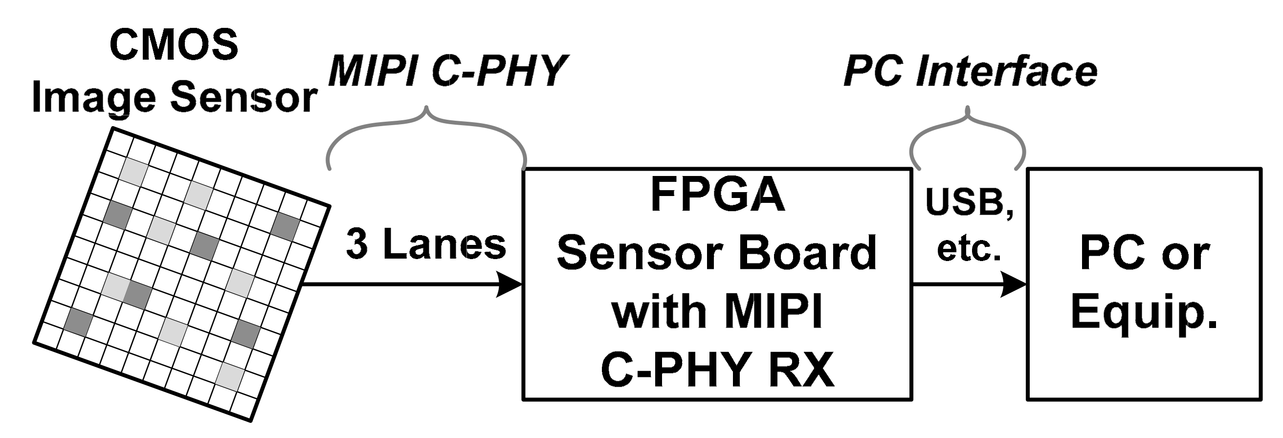
:1. Introduction
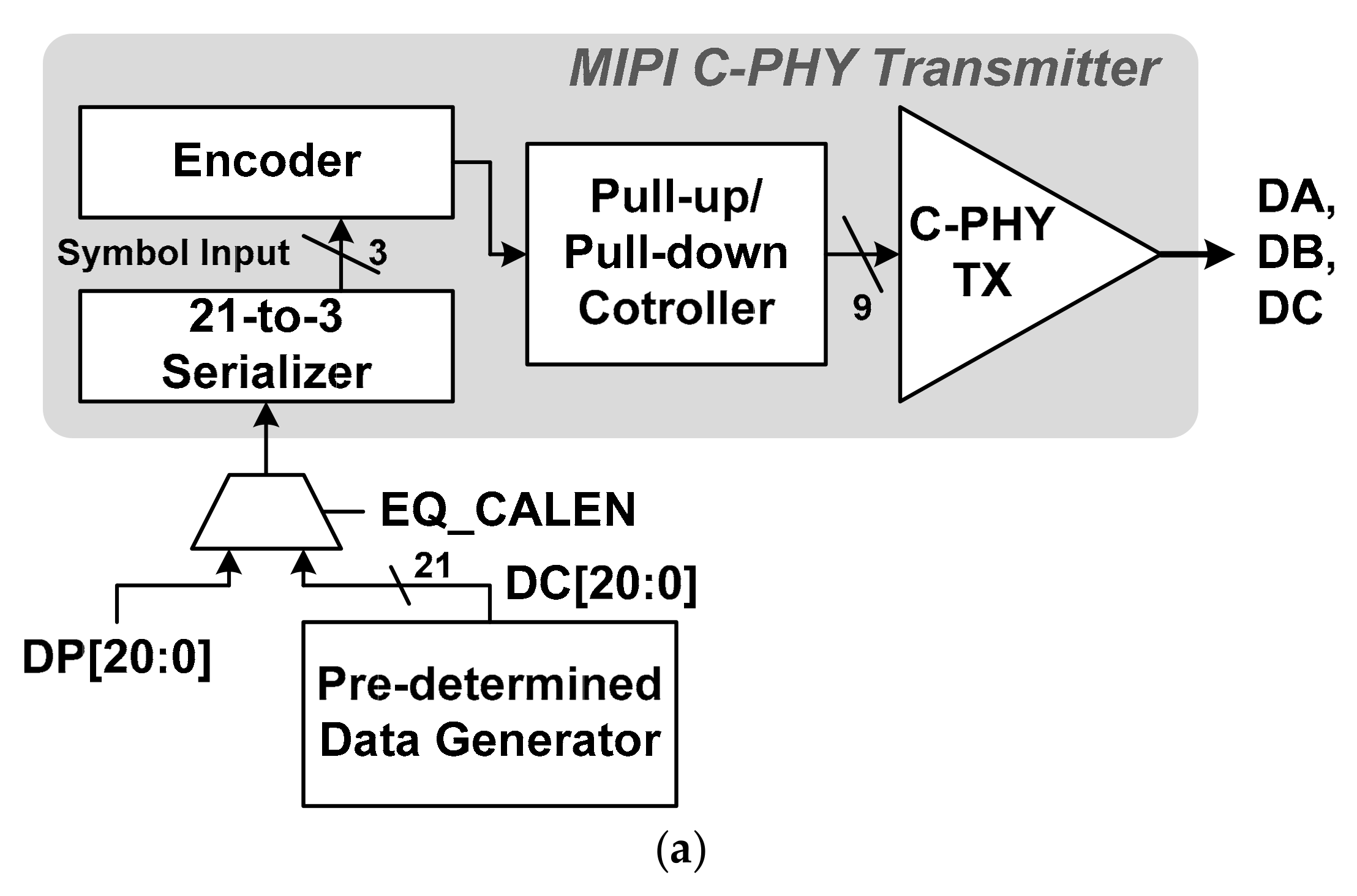
2. Pre-Determined Data for Adaptive Level-Dependent Equalization
3. MIPI C-PHY Receiver Chip
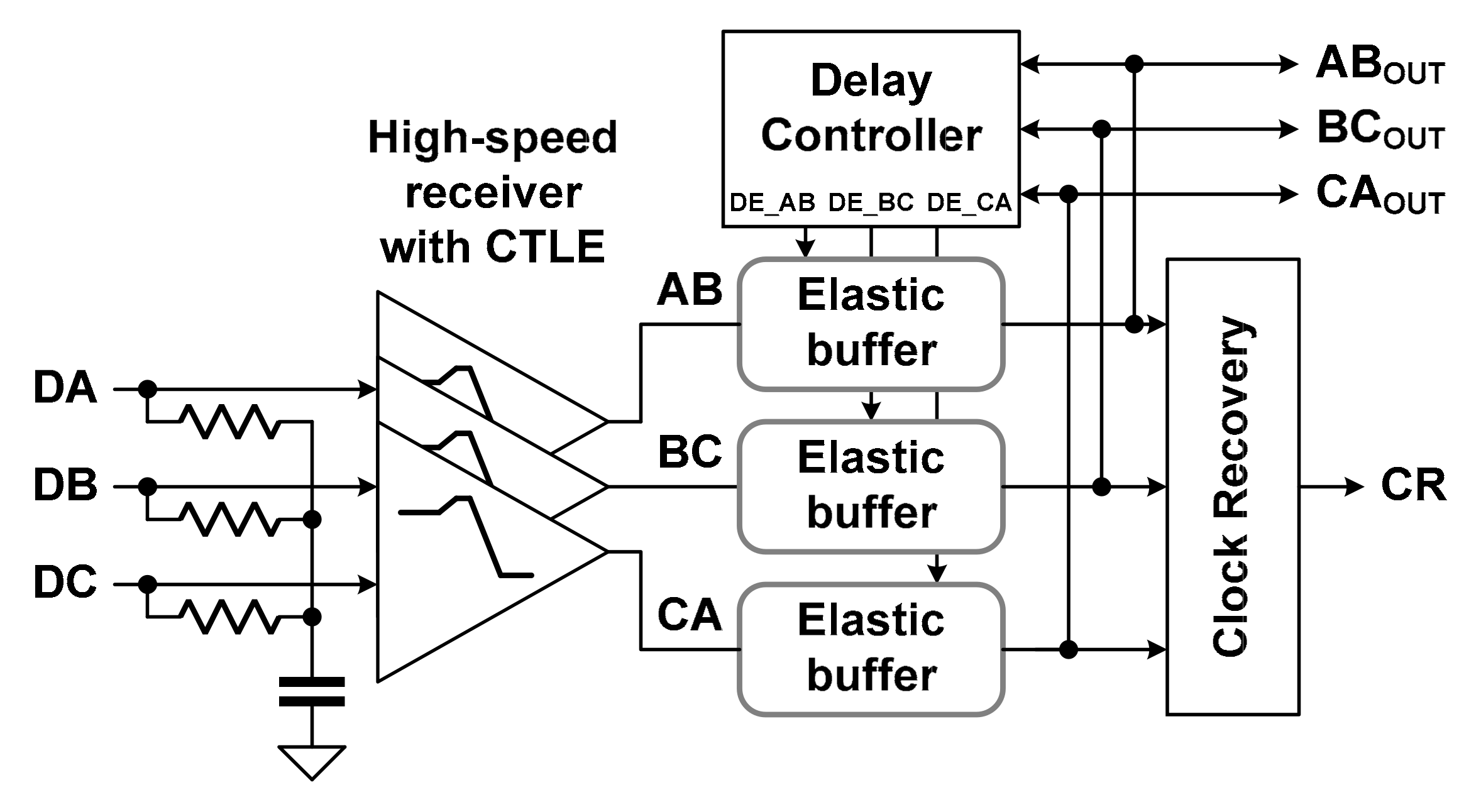
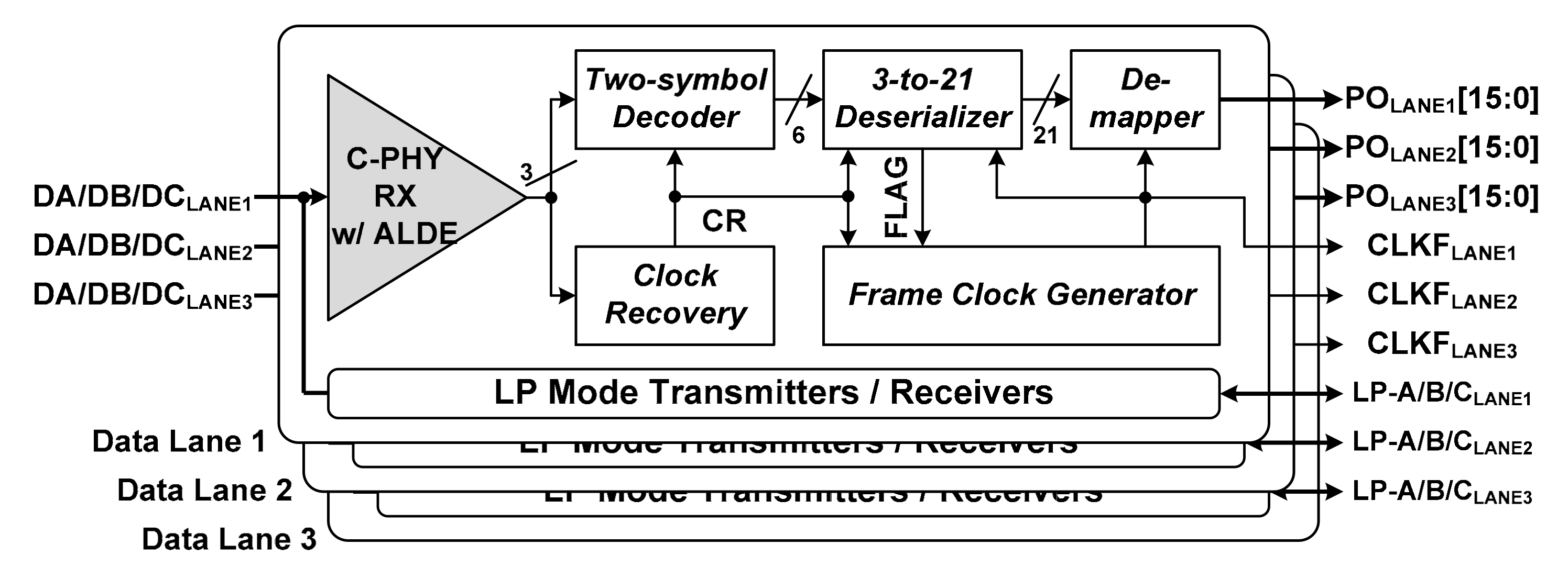
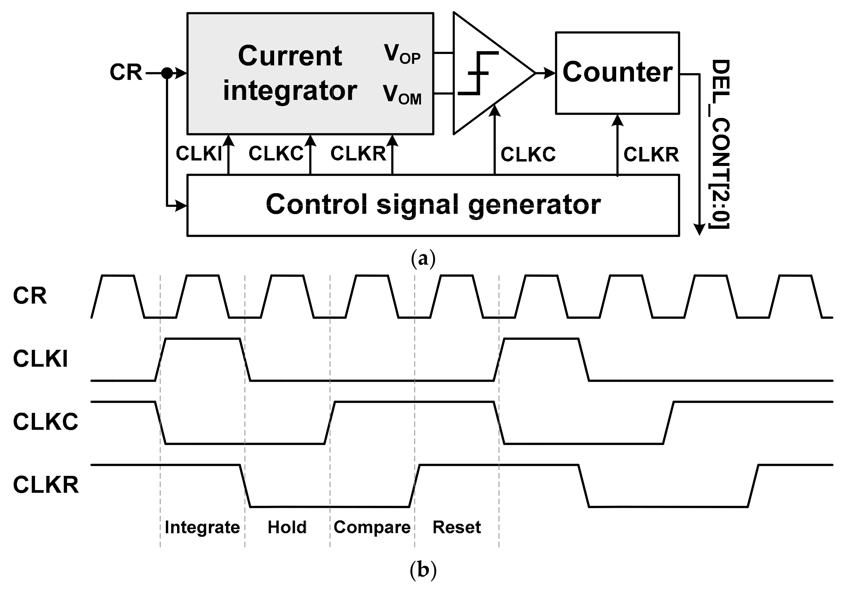
3.1. MIPI C-PHY Receiver
3.2. Adaptive Level-Dependent Equalizer
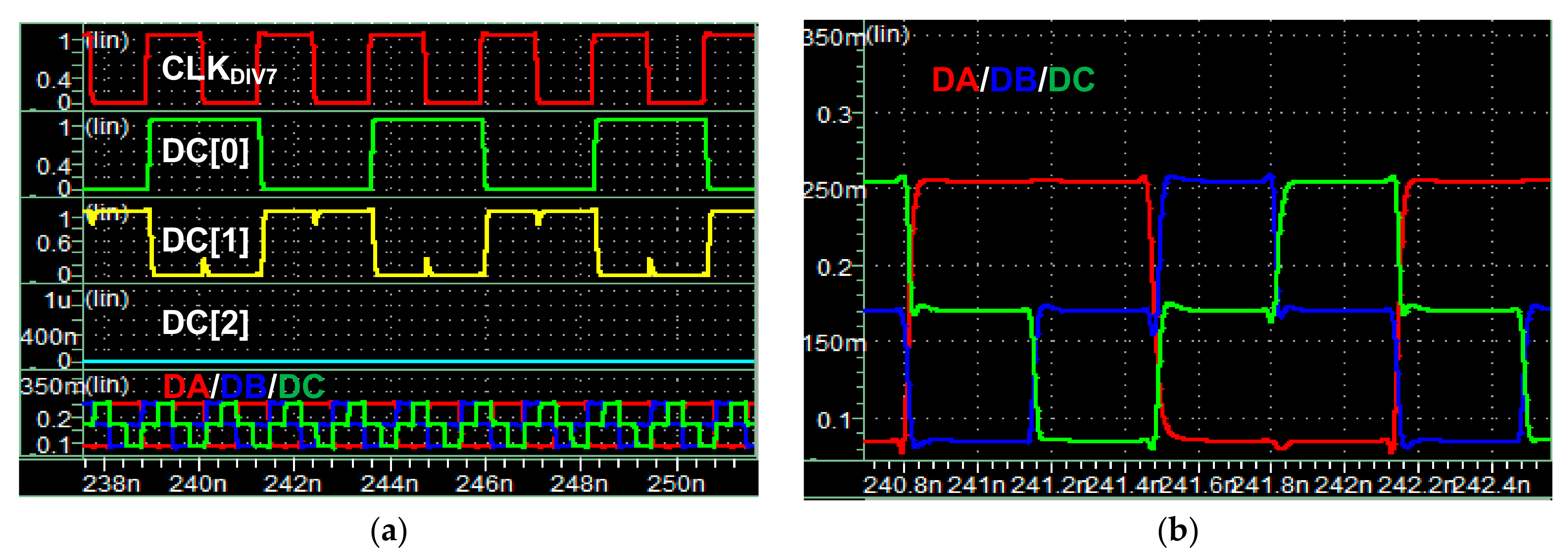
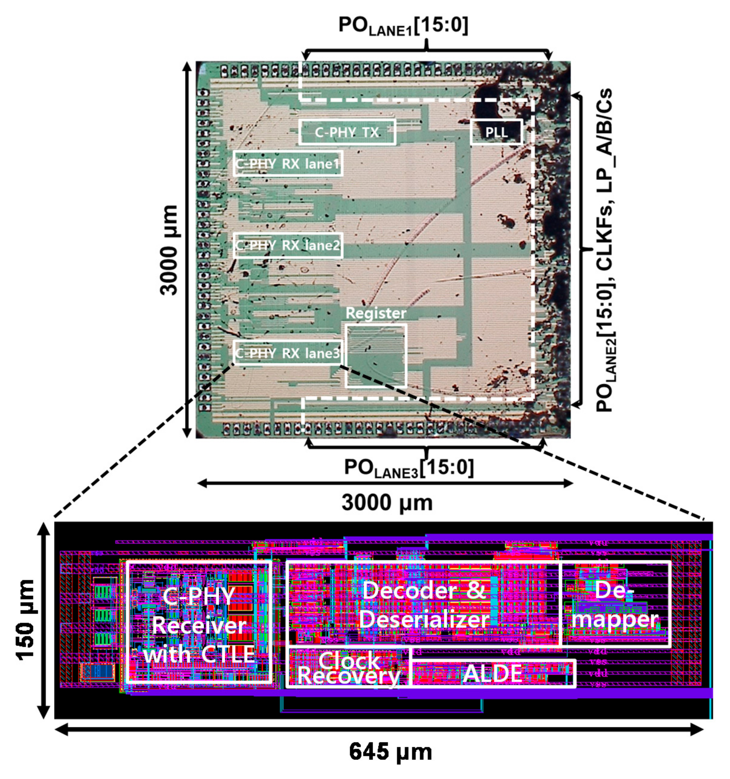
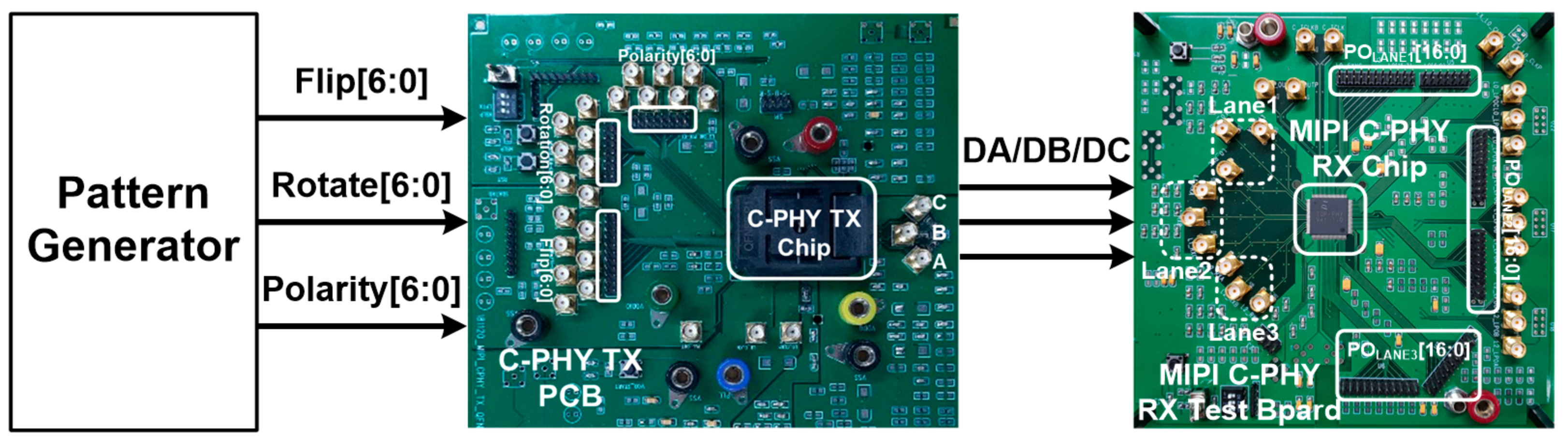
4. Implementation and Measurement Results of Proposed MIPI C-PHY Receiver
5. Conclusions
Author Contributions
Funding
Institutional Review Board Statement
Informed Consent Statement
Data Availability Statement
Acknowledgments
Conflicts of Interest
References
- Suzuki, A.; Shimamura, N.; Kainuma, T.; Kawazu, N.; Okada, C.; Oka, T.; Koiso, K.; Masagaki, A.; Yagasaki, Y.; Gonoi, S.; et al. A 1/1.7-inch 20Mpixel Back-Illuminated Stacked CMOS Image Sensor for New Imaging Applications. In Proceedings of the 2015 IEEE International Solid-State Circuits Conference Digest of Technical Papers, San Francisco, CA, USA, 22–26 February 2015; pp. 110–111. [Google Scholar]
- Kim, S.-H.; Shin, H.; Jeong, Y.; Lee, J.-H.; Choi, J.; Chun, J.-H. A 12-Gb/s Stacked Dual-Channel Interface for CMOS Image Sensor Systems. Sensors 2018, 18, 2709. [Google Scholar] [CrossRef] [PubMed] [Green Version]
- Jung, Y.J.; Venezia, V.C.; Lee, S.; Ai, C.Y.; Zhu, Y.; Yeung, K.W.; Park, G.; Choi, W.; Lin, Z.; Yang, W.-Z.; et al. A 64M CMOS Image Sensor using 0.7um pixel with high FWC and switchable conversion. In Proceedings of the 2020 IEEE International Electron Devices Meeting, San Francisco, CA, USA, 12–18 December 2020; pp. 335–338. [Google Scholar]
- Park, J.; Park, S.; Cho, K.; Lee, T.; Lee, C.; Kim, D.; Lee, B.; Kim, S.; Ji, H.-C.; Im, D.; et al. 1/2.74-inch 32Mpixel-Prototype CMOS Image Sensor with 0.64μ m Unit Pixels Separated by Full-Depth Deep-Trench Isolation. In Proceedings of the 2021 IEEE International Solid-State Circuits Conference Digest of Technical Papers, San Francisco, CA, USA, 13–22 February 2021; pp. 112–113. [Google Scholar]
- MIPI Alliance. MIPI Alliance Specification for D-PHY, Version 2.0. November 2015. Available online: https://www.mipi.org/specifications/d-phy (accessed on 23 November 2015).
- MIPI Alliance. MIPI Alliance Specification for C-PHY, Version 1.1. October 2015. Available online: https://www.mipi.org/specifications/c-phy (accessed on 7 October 2015).
- Choi, W.; Kim, T.; Shim, J.; Kim, H.; Han, G.; Chae, Y. A 1V 7.8mW 15.6Gb/s C-PHY transceiver using tri-level signaling for post-LPDDR4. In Proceedings of the 2017 IEEE International Solid-State Circuits Conference Digest of Technical Papers, San Francisco, CA, USA, 5–9 February 2017; pp. 402–403. [Google Scholar]
- Lee, P.-H.; Jang, Y.-C. A 20-Gb/s Receiver Bridge Chip with Auto-Skew Calibration for MIPI D-PHY Interface. IEEE Trans. Consumer Electron. 2019, 65, 484–492. [Google Scholar] [CrossRef]
- Kim, W.; Lee, M. A 92-μW/Gbps Self-Biased SLVS Receiver for MIPI D-PHY Applications. IEEE Trans. Circuits Syst. II Express Briefs (Early Access) 2021. [Google Scholar] [CrossRef]
- Lancheres, P.; Hafed, M. The MIPI C-PHY Standard: A Generalized Multiconductor Signaling Scheme. IEEE Solid-State Circuits Mag. 2019, 11, 69–77. [Google Scholar] [CrossRef]
- Poulton, J.W.; Wilson, J.M.; Turner, W.J.; Zimmer, B.; Chen, X.; Kudva, S.S.; Song, S.; Tell, S.G.; Nedovic, N.; Zhao, W.; et al. A 1.17pJ/b 25Gb/s/pin Ground-Referenced Single-Ended Serial Link for Off- and On-Package Communication in 16nm CMOS Using a Process- and Temperature-Adaptive Voltage Regulator. IEEE J. Solid-State Circuits 2019, 54, 43–54. [Google Scholar] [CrossRef]
- Chen, Y.; Mak, P.-I.; Wang, Y. A Highly-Scalable Analog Equalizer Using a Tunable and Current-Reusable Active Inductor for 10-Gb/s I/O Links. IEEE Trans. Very Large Integr. Syst. 2015, 23, 978–982. [Google Scholar] [CrossRef]
- Lee, P.-H.; Jang, Y.-C. A 6.84 Gbps/lane MIPI C-PHY Transceiver Bridge Chip with Level-Dependent Equalization. IEEE Trans. Circuits Syst. II Express Briefs 2020, 67, 2672–2676. [Google Scholar] [CrossRef]
- Choi, S. 3-GSymbol/s/lane MIPI C-PHY Receiver with Reduction of Channel Mismatch and Data-dependent Time Jitter. Master’s Thesis, Kumoh National Institute of Technology, Gumi, Korea, December 2019. [Google Scholar]
- Sidiropoulos, S.; Horowitz, M. A 700-Mb/s/pin CMOS signaling interface using current integrating receivers. IEEE J. Solid-State Circuits 1997, 32, 681–690. [Google Scholar] [CrossRef]
- Jang, Y.-C.; Bae, J.-H.; Park, H.-J. A Digital CMOS PWCL with Fixed-Delay Rising Edge and Digital Stability Control. IEEE Trans. Circuits Syst. II Express Briefs 2006, 53, 1063–1067. [Google Scholar] [CrossRef]
- Kim, T.-J.; Hwang, J.-I.; Lee, S.; Chun, S.; Ryu, S.-Y.; Lee, S.-J.; Cho, H.; Tak, W.; Kim, Y.-J.; Lee, H.; et al. A 14-Gb/s dual-mode receiver with MIPI D-PHY and C-PHY interfaces for mobile display drivers. J. Soc. Inf. Display 2020, 28, 535–547. [Google Scholar] [CrossRef]


| Reference | ISSCC’17 [7] | JSID’20 [17] | This Work | |
|---|---|---|---|---|
| Application | Memory interface | MIPI D-/C-PHY | MIPI C-PHY V1.1 | |
| Technology | 65 nm CMOS | 28 nm CMOS | 65 nm CMOS | |
| Supply | 1.0 V | 1.0 V | 1.2 V | |
| Operation mode | Receiver | Receiver | Receiver | |
| Data rate per lane | 6.85 Gsymbol/s (15.62 Gb/s) | 2.2 Gsymbol/s (5.02 Gb/s) | 3.0 Gsymbol/s (6.84 Gb/s) | |
| Function blocks for HS mode | Receiver | Receiver Clock recovery Symbol decoder Deserializer | Receiver Clock recovery Symbol decoder Deserializer De-mapper Parallel transmitter | |
| LP mode | No | Yes | Yes | |
| Channel for measurement | 4 cm FR4 | 15.24 cm PCB | 10.16 cm FR4 | |
| Eye opening of data | w/o Eq. | closed | - | 0.58 UI |
| w/ Eq. | 0.51 UI | 0 | 0.61 UI | |
| ∆tpk-to-pk of recovered clock | w/o Eq. | N/A | - | 96 ps |
| w/ Eq. | N/A | - | 62 ps | |
| Power per lane [mW/Gb/s] | - 0.22 1 | 1.96 ≈1.06 1 | 2.15 0.54 1 | |
Publisher’s Note: MDPI stays neutral with regard to jurisdictional claims in published maps and institutional affiliations. |
© 2021 by the authors. Licensee MDPI, Basel, Switzerland. This article is an open access article distributed under the terms and conditions of the Creative Commons Attribution (CC BY) license (https://creativecommons.org/licenses/by/4.0/).
Share and Cite
Choi, S.; Song, C.; Jang, Y.-C. A 3.0 Gsymbol/s/lane MIPI C-PHY Receiver with Adaptive Level-Dependent Equalizer for Mobile CMOS Image Sensor. Sensors 2021, 21, 5197. https://doi.org/10.3390/s21155197
Choi S, Song C, Jang Y-C. A 3.0 Gsymbol/s/lane MIPI C-PHY Receiver with Adaptive Level-Dependent Equalizer for Mobile CMOS Image Sensor. Sensors. 2021; 21(15):5197. https://doi.org/10.3390/s21155197
Chicago/Turabian StyleChoi, Seokwon, Changmin Song, and Young-Chan Jang. 2021. "A 3.0 Gsymbol/s/lane MIPI C-PHY Receiver with Adaptive Level-Dependent Equalizer for Mobile CMOS Image Sensor" Sensors 21, no. 15: 5197. https://doi.org/10.3390/s21155197
APA StyleChoi, S., Song, C., & Jang, Y.-C. (2021). A 3.0 Gsymbol/s/lane MIPI C-PHY Receiver with Adaptive Level-Dependent Equalizer for Mobile CMOS Image Sensor. Sensors, 21(15), 5197. https://doi.org/10.3390/s21155197