
The Heterostructures of CuO and SnOx for NO2 Detection

 , , , , ,
Abstract
:1. Introduction
2. Materials and Methods
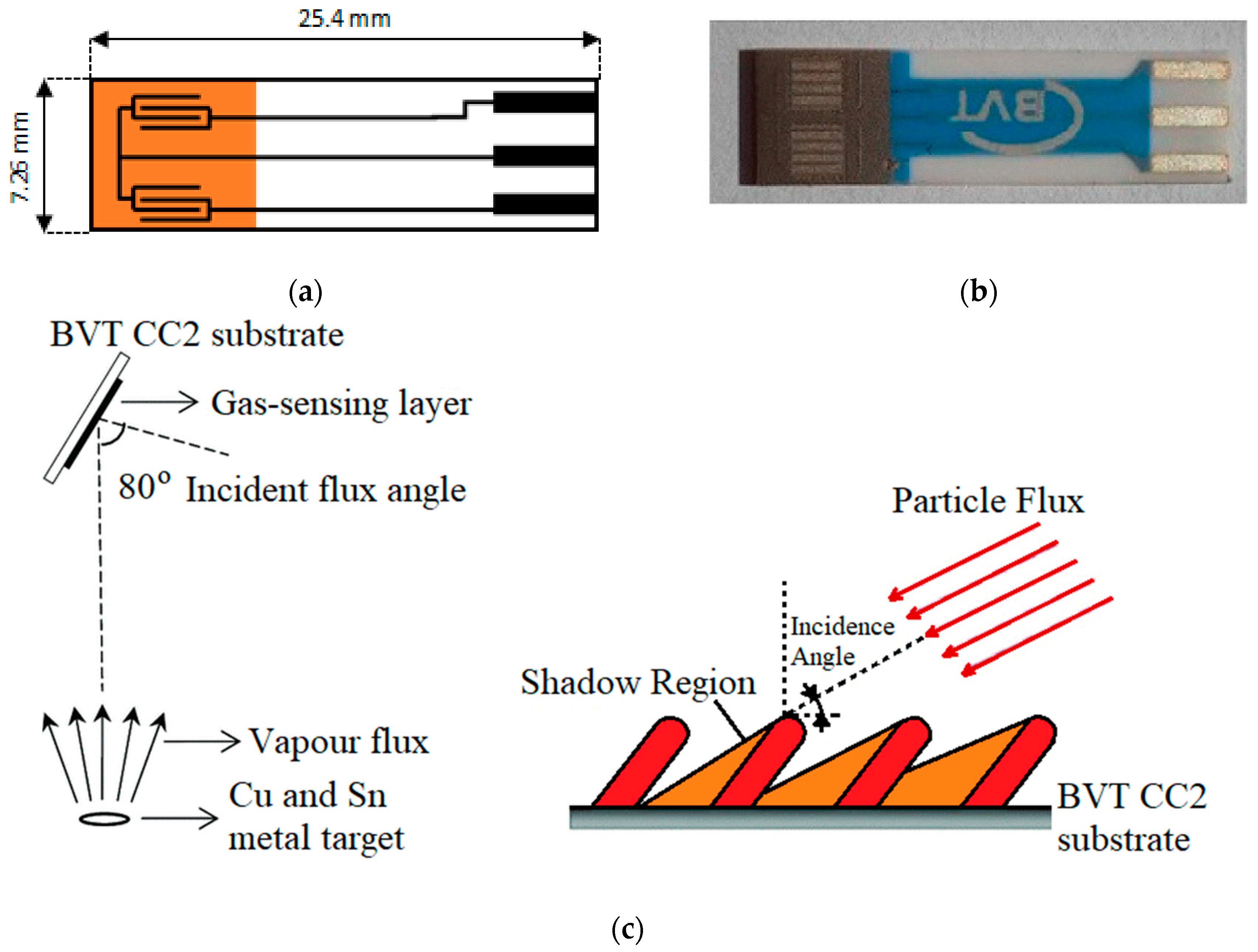
2.1. Gas Sensor Substrates
2.2. Gas-Sensitive Layer Deposition
2.2.1. Tin Oxide
2.2.2. Copper Oxide
2.3. Gas-Sensing Measurements
2.3.1. Measurements of Resistance Changes with Direct Current (DC)
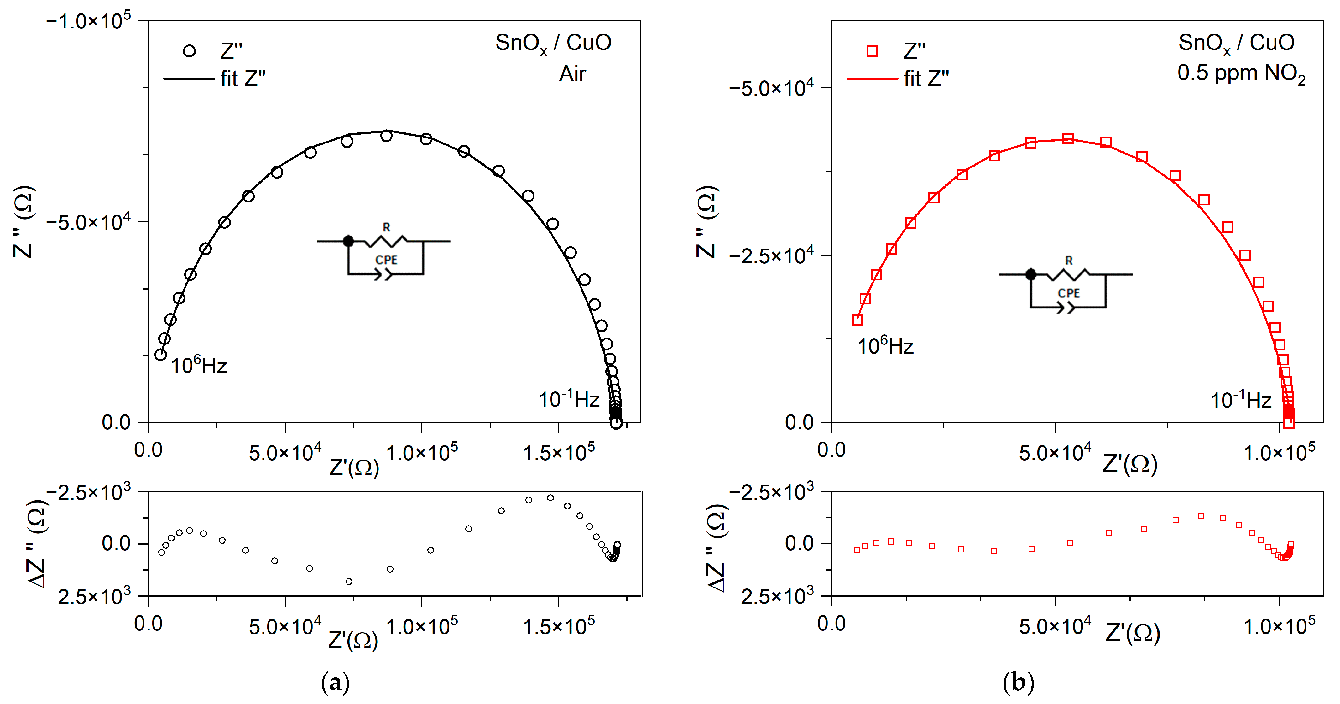
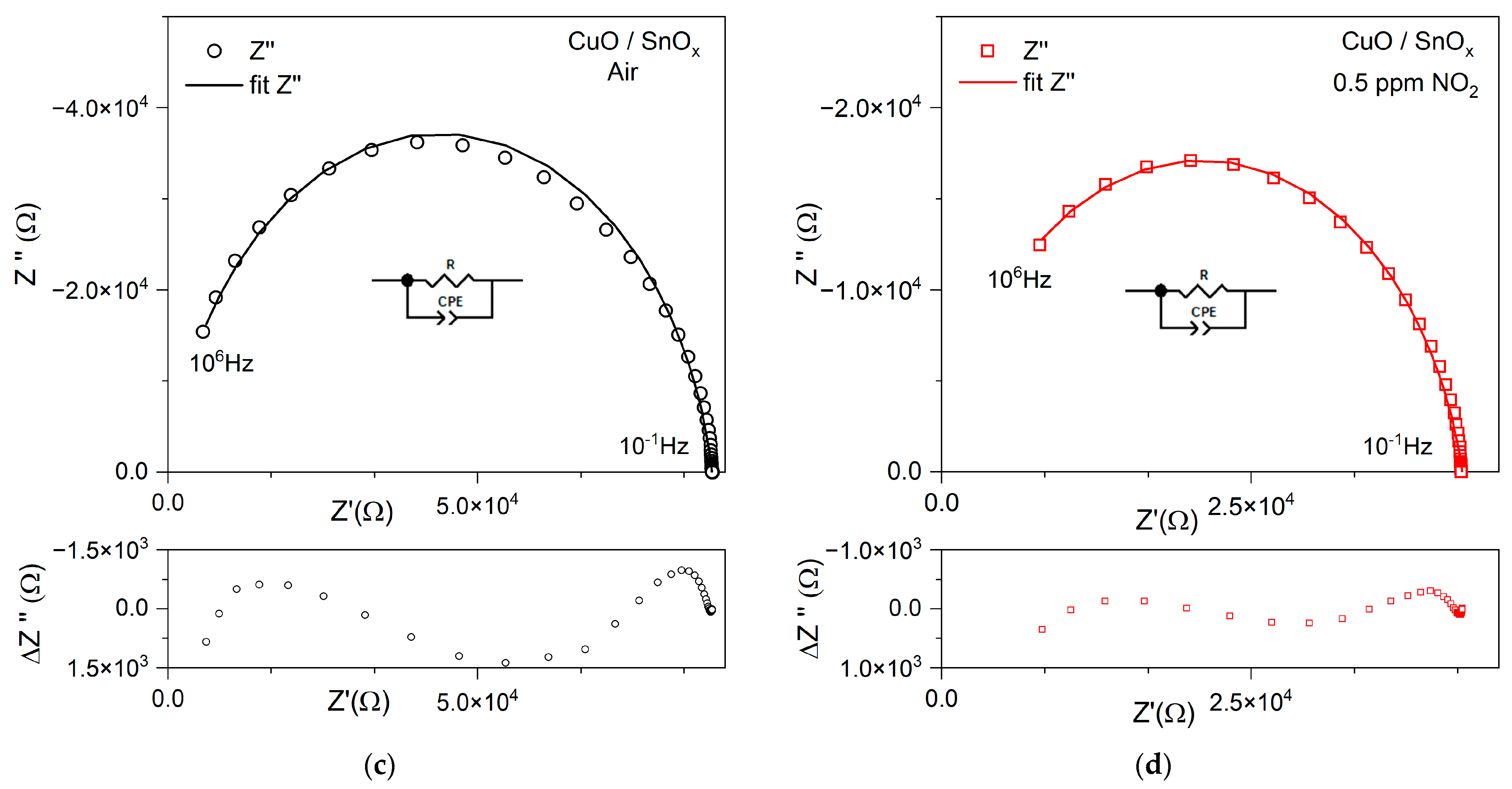
2.3.2. Measurements of Electrical Properties with Alternating Current (AC)
2.4. Material Characterization
3. Results
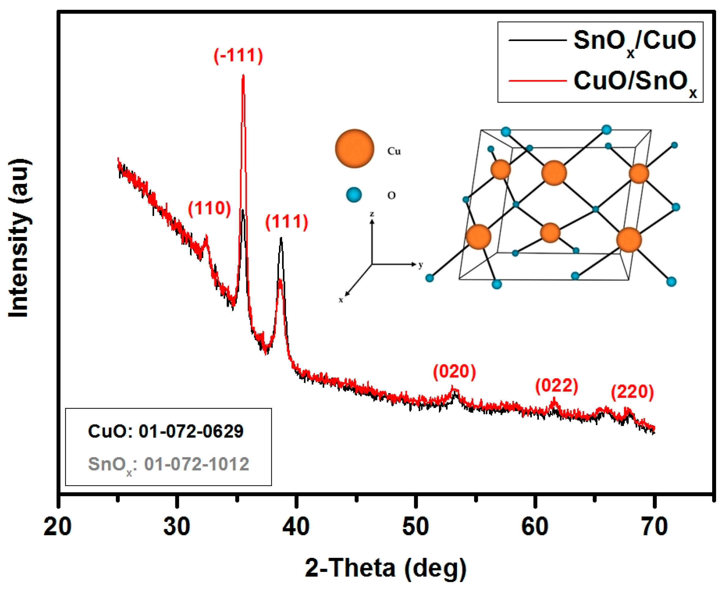
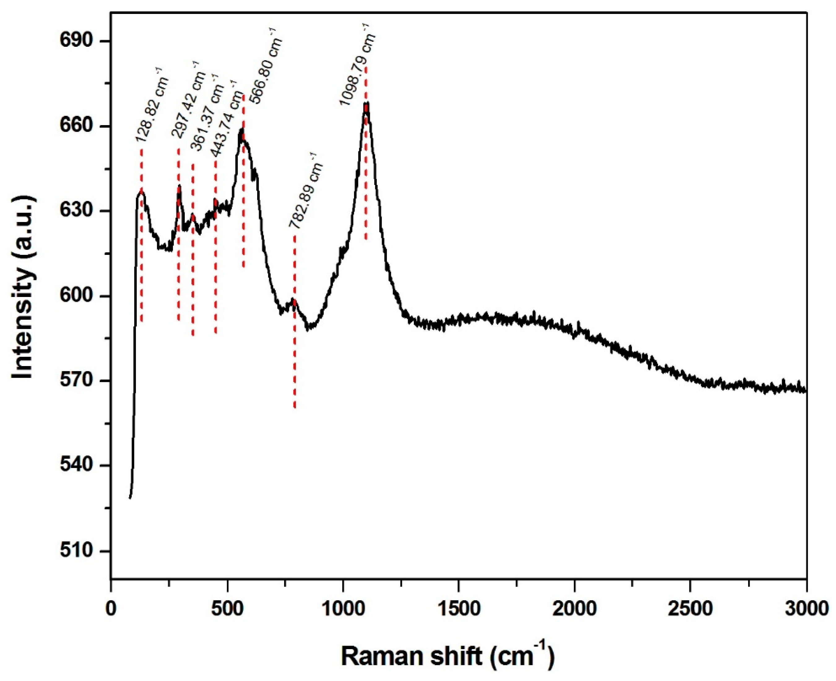
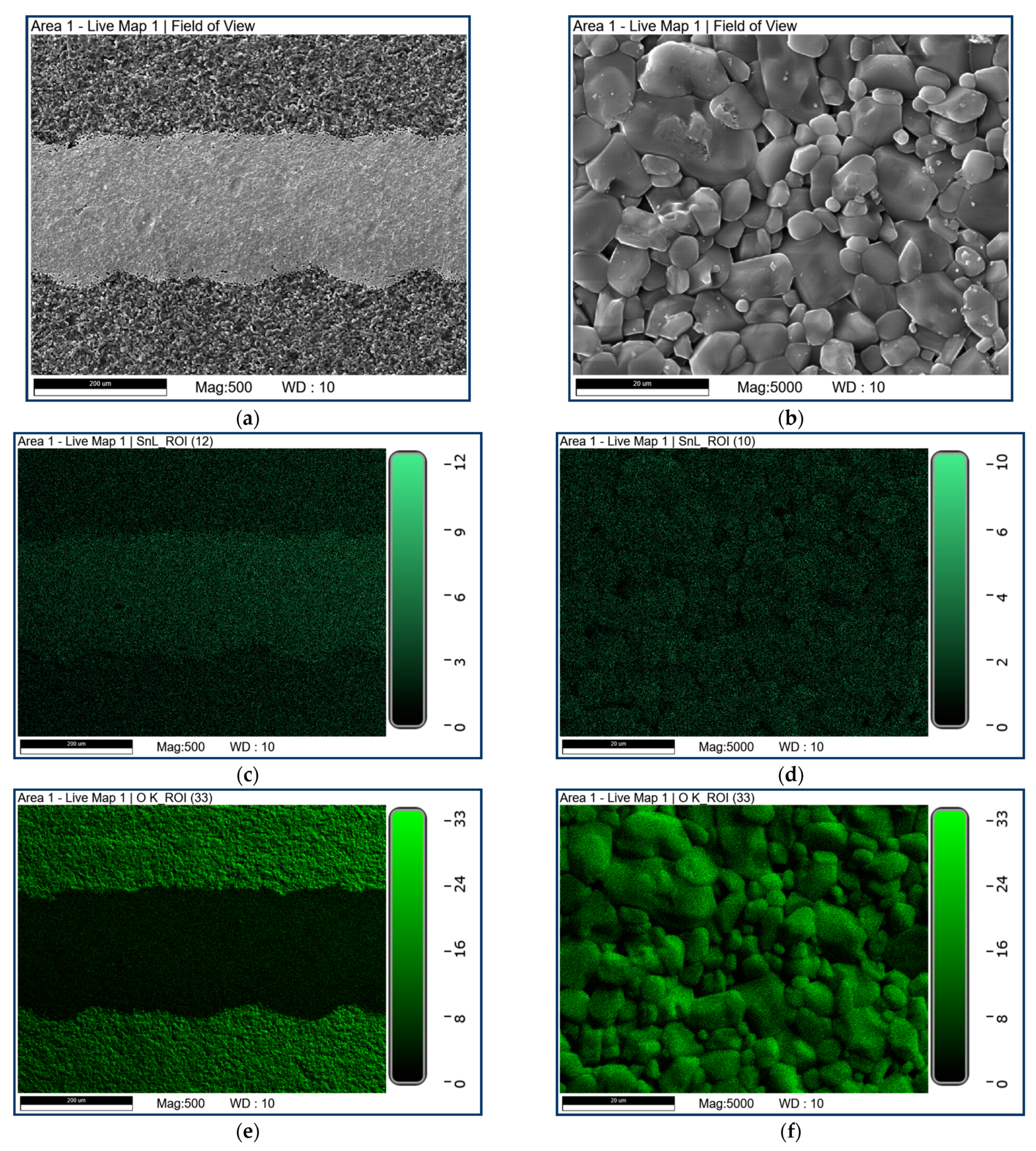
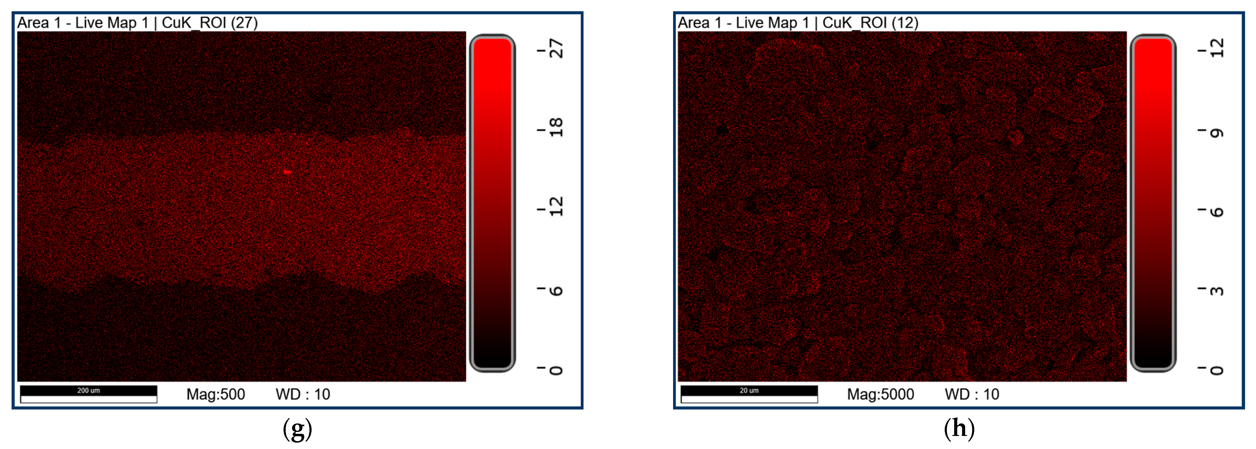
3.1. Characterization Results
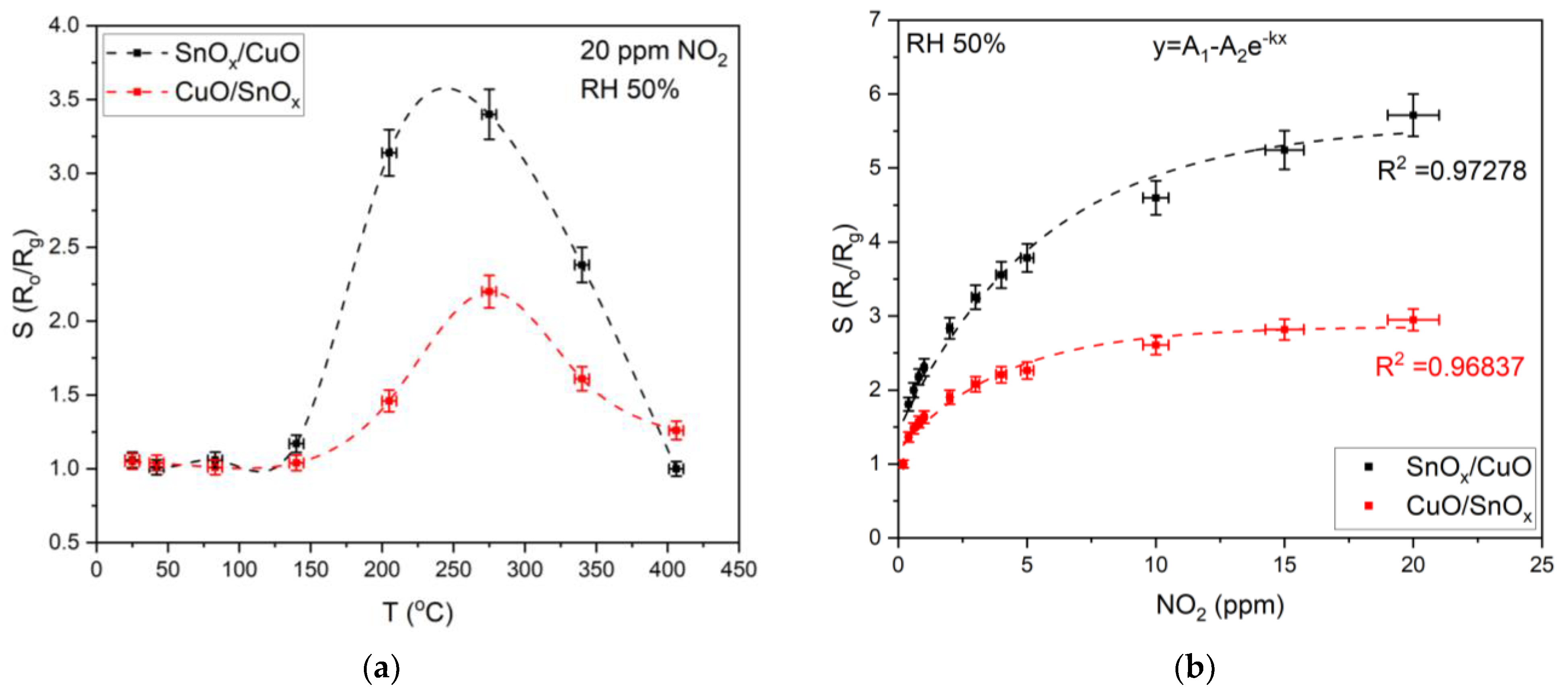
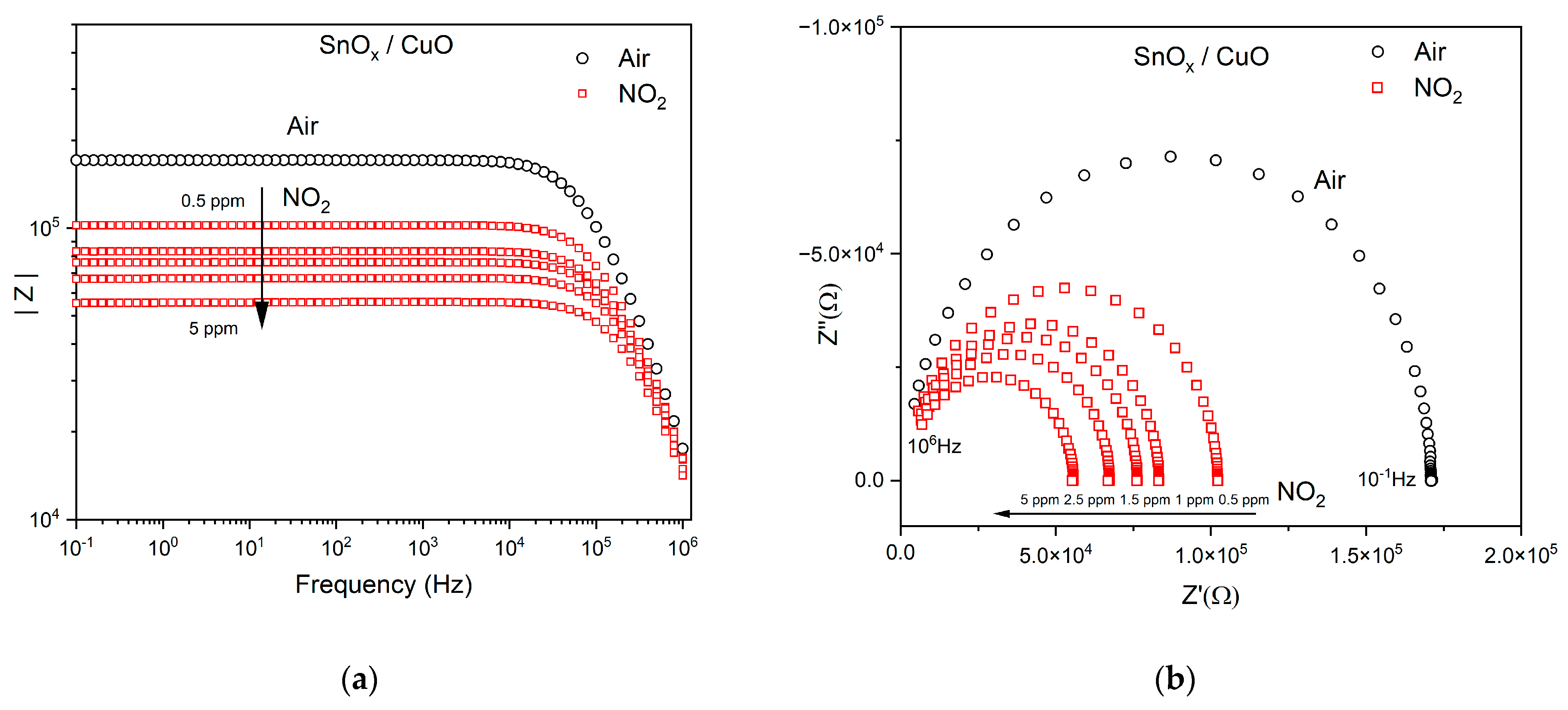
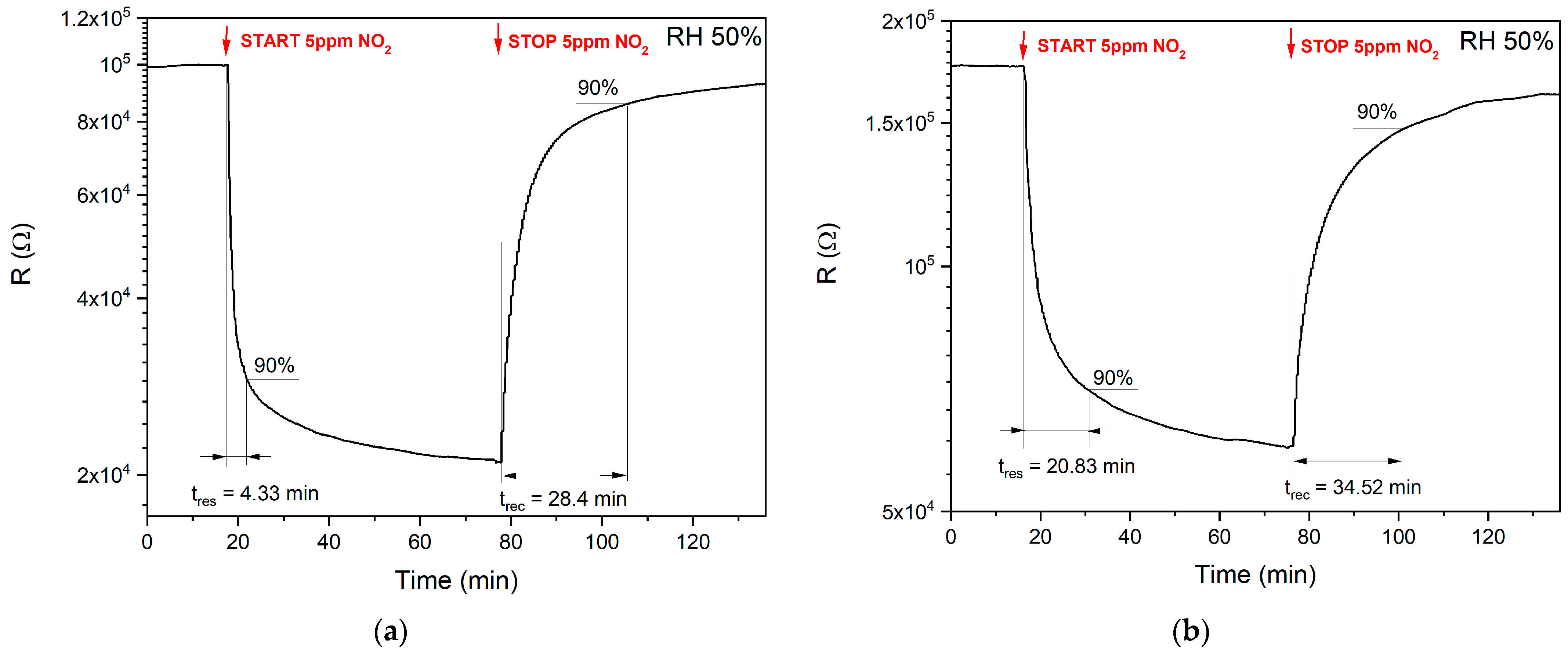
3.2. Gas-Sensing Characteristics
3.2.1. NO2
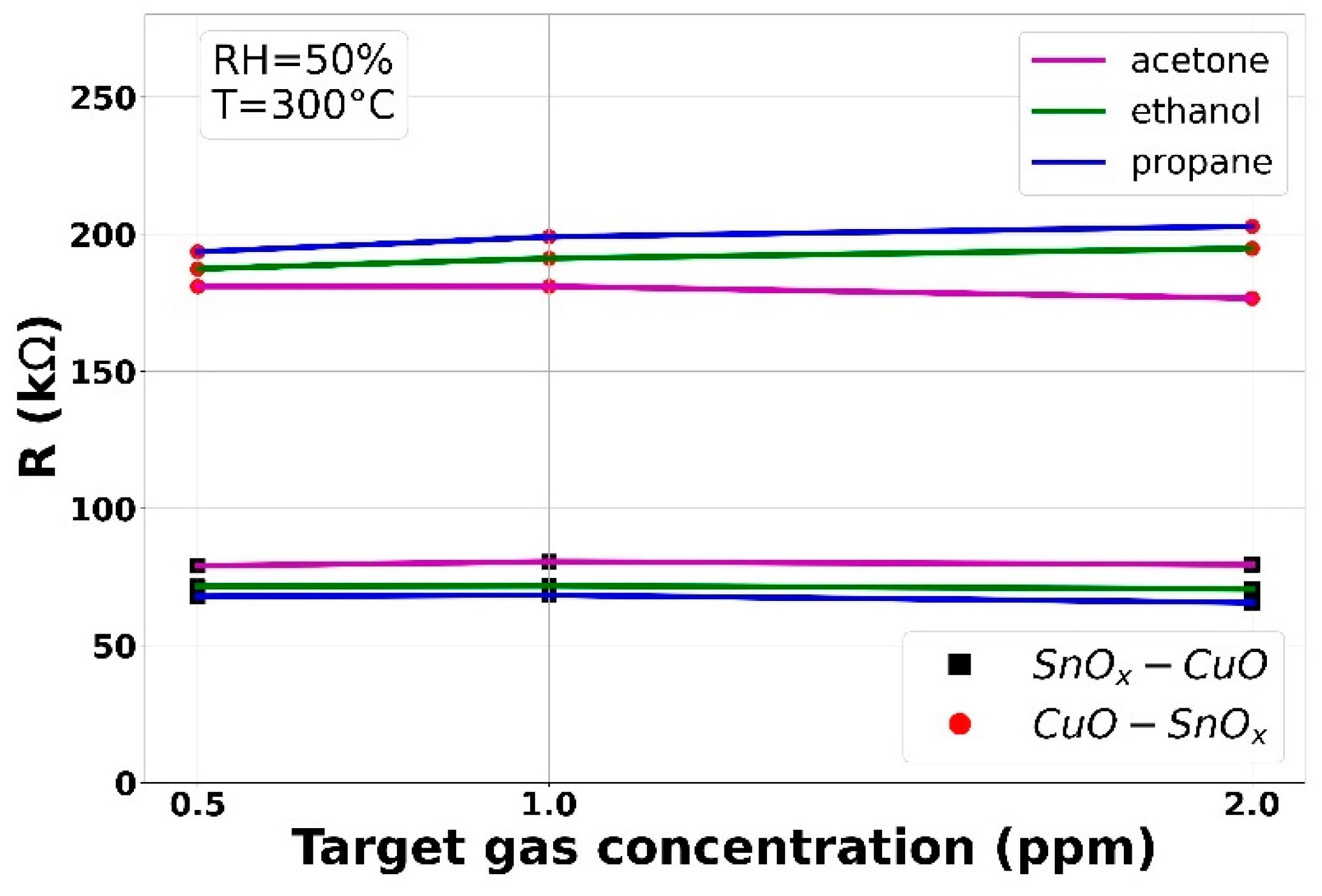
3.2.2. VOCs
3.2.3. Response and Recovery Times
4. Conclusions
Supplementary Materials
Author Contributions
Funding
Institutional Review Board Statement
Informed Consent Statement
Data Availability Statement
Conflicts of Interest
References
- Gas Sensor Market Size, Share|Industry Trends and Growth by 2027. Available online: https://www.alliedmarketresearch.com/gas-sensors-market (accessed on 6 February 2021).
- Gas Sensors Market by Analysis, Type, Technology, Technology, Output Type, Product Type, Application|COVID-19 Impact Analysis|MarketsandMarketsTM. Available online: https://www.marketsandmarkets.com/Market-Reports/gas-sensor-market-245141093.html (accessed on 13 April 2021).
- Global Gas Sensor Market Size & Share Report, 2021–2028. Available online: https://www.grandviewresearch.com/industry-analysis/gas-sensors-market (accessed on 6 February 2021).
- WHO. Formaldehyde. In Selected Pollutants. WHO Guidelines for Indoor Air Quality; WHO, Regional Office for Europe: Copenhagen, Denmark, 2010; pp. 103–156. ISBN 978-92-890-02134. Available online: http://www.euro.who.int/__data/assets/pdf_file/0009/128169/e94535.pdf?ua=1 (accessed on 6 April 2021).
- World Health Organization. Ambient (Outdoor) Air Pollution. Available online: https://www.who.int/news-room/fact-sheets/detail/ambient-(outdoor)-air-quality-and-health (accessed on 3 March 2020).
- EUR-Lex—L:2008:152:TOC—EN—EUR-Lex. Available online: https://eur-lex.europa.eu/legal-content/EN/TXT/?uri=OJ:L:2008:152:TOC (accessed on 14 April 2021).
- CDC—Immediately Dangerous to Life or Health Concentrations (IDLH): Nitrogen Dioxide—NIOSH Publications and Products. Available online: https://www.cdc.gov/niosh/idlh/10102440.html (accessed on 16 April 2021).
- Commission Regulation (EU) 2018/1832 of 5 November 2018 Amending Directive 2007/46/EC of the European Parliament and of the Council, Commission Regulation (EC) No 692/2008 and Commission Regulation (EU) 2017/1151 for the Purpose of Improving the Emission Type Approval Tests and Procedures for Light Passenger and Commercial Vehicles, Including Those for in-Service Conformity and Real-Driving Emissions and Introducing Devices for Monitoring the Consumption of Fuel and Electric Energy (Text with EEA Relevance). 2018, Volume 301. Available online: https://eur-lex.europa.eu/legal-content/EN/TXT/PDF/?uri=CELEX:32018R1832&from=FR (accessed on 7 April 2021).
- Directive 2012/13/EU of the European Parliament and of the Council of 22 May 2012 on the Right to Information in Criminal Proceedings. 2012. Available online: https://eur-lex.europa.eu/legal-content/EN/TXT/?uri=CELEX:32012L0013 (accessed on 7 April 2021).
- EUR-Lex—32012R0459—EN—EUR-Lex. Available online: https://eur-lex.europa.eu/eli/reg/2012/459/oj (accessed on 17 April 2021).
- Ligterink, N.E.; Kadijk, G.A.; Mensch, P.V.; Smokers, R.T.M. NOx Emissions of Euro 5 and Euro 6 Diesel Passenger Cars—Test Results in the Lab and on the Road; TNO: Delft, The Netherlands, 2016. [Google Scholar] [CrossRef]
- Aleixandre, M.; Gerboles, M. Review of Small Commercial Sensors for Indicative Monitoring of Ambient Gas. Chem. Eng. Trans. 2012, 30, 1–6. [Google Scholar]
- Choi, M.S.; Gil Na, H.; Mirzaei, A.; Bang, J.H.; Oum, W.; Han, S.; Choi, S.-W.; Kim, M.; Jin, C.; Kim, S.S.; et al. Room-temperature NO2 sensor based on electrochemically etched porous silicon. J. Alloys Compd. 2019, 811, 151975. [Google Scholar] [CrossRef]
- Zhao, J.; Wen, X.; Huang, Y.; Liu, P. Piezoelectric circuitry tailoring for resonant mass sensors providing ultra-high impedance sensitivity. Sens. Actuators A Phys. 2019, 285, 275–282. [Google Scholar] [CrossRef]
- Wasisto, H.S.; Merzsch, S.; Stranz, A.; Waag, A.; Uhde, E.; Salthammer, T.; Peiner, E. Silicon resonant nanopillar sensors for airborne titanium dioxide engineered nanoparticle mass detection. Sens. Actuators B Chem. 2013, 189, 146–156. [Google Scholar] [CrossRef]
- Jia, H.; Xu, P.; Li, X. Integrated Resonant Micro/Nano Gravimetric Sensors for Bio/Chemical Detection in Air and Liquid. Micromachines 2021, 12, 645. [Google Scholar] [CrossRef]
- Alunda, B.O.; Lee, Y.J. Review: Cantilever-Based Sensors for High Speed Atomic Force Microscopy. Sensors 2020, 20, 4784. [Google Scholar] [CrossRef]
- Zhao, J.; Sun, C.; Kacem, N.; Wang, H.; Gao, R.; Liu, P.; Huang, Y. A nonlinear resonant mass sensor with enhanced sensitivity and resolution incorporating compressed bistable beam. J. Appl. Phys. 2018, 124, 164503. [Google Scholar] [CrossRef] [Green Version]
- Akbari, E.; Jahanbin, K.; Afroozeh, A.; Yupapin, P.; Buntat, Z. Brief review of monolayer molybdenum disulfide application in gas sensor. Phys. B Condens. Matter 2018, 545, 510–518. [Google Scholar] [CrossRef]
- Rana, M.; Ibrahim, D.S.; Asyraf, M.M.; Jarin, S.; Tomal, A. A review on recent advances of CNTs as gas sensors. Sens. Rev. 2017, 37, 127–136. [Google Scholar] [CrossRef]
- Toda, K.; Furue, R.; Hayami, S. Recent progress in applications of graphene oxide for gas sensing: A review. Anal. Chim. Acta 2015, 878, 43–53. [Google Scholar] [CrossRef]
- Nikolic, M.V.; Milovanovic, V.; Vasiljevic, Z.Z.; Stamenkovic, Z. Semiconductor Gas Sensors: Materials, Technology, Design, and Application. Sensors 2020, 20, 6694. [Google Scholar] [CrossRef]
- Dey, A. Semiconductor metal oxide gas sensors: A review. Mater. Sci. Eng. B 2018, 229, 206–217. [Google Scholar] [CrossRef]
- Nazemi, H.; Joseph, A.; Park, J.; Emadi, A. Advanced Micro- and Nano-Gas Sensor Technology: A Review. Sensors 2019, 19, 1285. [Google Scholar] [CrossRef] [Green Version]
- Zhang, C.; Liu, G.; Geng, X.; Wu, K.; Debliquy, M. Metal oxide semiconductors with highly concentrated oxygen vacancies for gas sensing materials: A review. Sens. Actuators A Phys. 2020, 309, 112026. [Google Scholar] [CrossRef]
- Hung, C.M.; Le, D.T.T.; Van Hieu, N. On-chip growth of semiconductor metal oxide nanowires for gas sensors: A review. J. Sci. Adv. Mater. Devices 2017, 2, 263–285. [Google Scholar] [CrossRef]
- Comini, E. Metal oxides nanowires chemical/gas sensors: Recent advances. Mater. Today Adv. 2020, 7, 100099. [Google Scholar] [CrossRef]
- Yang, S.; Lei, G.; Xu, H.; Lan, Z.; Wang, Z.; Gu, H. Metal Oxide Based Heterojunctions for Gas Sensors: A Review. Nanomaterials 2021, 11, 1026. [Google Scholar] [CrossRef]
- Wang, Y.; Duan, L.; Deng, Z.; Liao, J. Electrically Transduced Gas Sensors Based on Semiconducting Metal Oxide Nanowires. Sensors 2020, 20, 6781. [Google Scholar] [CrossRef]
- Zappa, D.; Galstyan, V.; Kaur, N.; Arachchige, H.M.M.; Sisman, O.; Comini, E. “Metal oxide -based heterostructures for gas sensors”—A review. Anal. Chim. Acta 2018, 1039, 1–23. [Google Scholar] [CrossRef]
- Szafraniak, B.; Fuśnik, Ł.; Xu, J.; Gao, F.; Brudnik, A.; Rydosz, A. Semiconducting Metal Oxides: SrTiO3, BaTiO3 and BaSrTiO3 in Gas-Sensing Applications: A Review. Coatings 2021, 11, 185. [Google Scholar] [CrossRef]
- Ciobota, C.; Piticescu, R.; Neagoe, C.; Tudor, I.; Matei, A.; Dragut, D.; Sobetkii, A.; Anghel, E.; Stanoiu, A.; Simion, C.; et al. Nanostructured Cobalt Doped Barium Strontium Titanate Thin Films with Potential in CO2 Detection. Materials 2020, 13, 4797. [Google Scholar] [CrossRef]
- Hu, Y.; Tan, O.K.; Cao, W.; Zhu, W. A low temperature nano-structured SrTiO3 thick film oxygen gas sensor. Ceram. Int. 2004, 30, 1819–1822. [Google Scholar] [CrossRef]
- Maziarz, W.; Rydosz, A.; Pisarkiewicz, T.; Domański, K.; Grabiec, P. Gas-sensitive Properties of ZnO Nanorods/Nanowires Obtained by Electrodeposition and Electrospinning Methods. Procedia Eng. 2012, 47, 841–844. [Google Scholar] [CrossRef] [Green Version]
- Rydosz, A.; Staszek, K.; Brudnik, A.; Gruszczynski, S. Tin Dioxide Thin Film with UV-enhanced Acetone Detection in Microwave Frequency Range. Micromachines 2019, 10, 574. [Google Scholar] [CrossRef] [Green Version]
- Rydosz, A.; Dyndał, K.; Kollbek, K.; Andrysiewicz, W.; Sitarz, M.; Marszałek, K. Structure and optical properties of the WO3 thin films deposited by the GLAD magnetron sputtering technique. Vacuum 2020, 177, 109378. [Google Scholar] [CrossRef]
- Rydosz, A.; Dyndał, K.; Andrysiewicz, W.; Grochala, D.; Marszałek, K. GLAD Magnetron Sputtered Ultra-Thin Copper Oxide Films for Gas-Sensing Application. Coatings 2020, 10, 378. [Google Scholar] [CrossRef] [Green Version]
- Eranna, G. Metal Oxide Nanostructures as Gas Sensing Devices; Informa UK Limited: London, UK, 2016. [Google Scholar]
- Sun, Y.-F.; Liu, S.-B.; Meng, F.-L.; Liu, J.-H.; Jin, Z.; Kong, L.-T. Metal Oxide Nanostructures and Their Gas Sensing Properties: A Review. Sensors 2012, 12, 2610–2631. [Google Scholar] [CrossRef] [Green Version]
- Bag, A.; Lee, N.-E. Gas sensing with heterostructures based on two-dimensional nanostructured materials: A review. J. Mater. Chem. C 2019, 7, 13367–13383. [Google Scholar] [CrossRef]
- Pisarkiewicz, T.; Maziarz, W.; Małolepszy, A.; Stobiński, L.; Michoń, D.A.; Szkudlarek, A.; Pisarek, M.; Kanak, J.; Rydosz, A. Nitrogen Dioxide Sensing using Multilayer Structure of Reduced Graphene Oxide and α-Fe2O3. Sensors 2021, 21, 1011. [Google Scholar] [CrossRef]
- Alev, O.; Kılıç, A.; Çakırlar, Ç.; Büyükköse, S.; Öztürk, Z.Z. Gas Sensing Properties of p-Co3O4/n-TiO2 Nanotube Heterostructures. Sensors 2018, 18, 956. [Google Scholar] [CrossRef] [Green Version]
- Chatterjee, S.G.; Chatterjee, S.; Ray, A.K.; Chakraborty, A.K. Graphene–metal oxide nanohybrids for toxic gas sensor: A review. Sens. Actuators B Chem. 2015, 221, 1170–1181. [Google Scholar] [CrossRef]
- Kurt, J. Lesker Company. Available online: https://www.lesker.com/newweb/deposition_materials/depositionmaterials_sputtertargets_1.cfm?pgid=cu1 (accessed on 29 April 2021).
- Rydosz, A.; Brudnik, A.; Staszek, K. Metal Oxide Thin Films Prepared by Magnetron Sputtering Technology for Volatile Organic Compound Detection in the Microwave Frequency Range. Materials 2019, 12, 877. [Google Scholar] [CrossRef] [PubMed] [Green Version]
- Rydosz, A. The Use of Copper Oxide Thin Films in Gas-Sensing Applications. Coatings 2018, 8, 425. [Google Scholar] [CrossRef] [Green Version]
- Rydosz, A.; Kollbek, K.; Kim-Ngan, N.-T.H.; Czapla, A.; Brudnik, A. Optical diagnostics of the magnetron sputtering process of copper in an argon–oxygen atmosphere. J. Mater. Sci. Mater. Electron. 2020, 31, 11624–11636. [Google Scholar] [CrossRef]
- Pisarkiewicz, T.; Maziarz, W.; Małolepszy, A.; Stobiński, L.; Michoń, D.; Rydosz, A. Multilayer Structure of Reduced Graphene Oxide and Copper Oxide as a Gas Sensor. Coatings 2020, 10, 1015. [Google Scholar] [CrossRef]
- Wang, C.; Yin, L.; Zhang, L.; Xiang, D.; Gao, R. Metal Oxide Gas Sensors: Sensitivity and Influencing Factors. Sensors 2010, 10, 2088–2106. [Google Scholar] [CrossRef] [Green Version]
- Dufour, N.; Veyrac, Y.; Menini, P.; Blanc, F.; Talhi, C.; Franc, B.; Ganibal, C.; Wartelle, C.; Aguir, K. Increasing the sensitivity and selectivity of Metal Oxide gas sensors by controlling the sensitive layer polarization. In Proceedings of the 2012 IEEE Sensors, Taipei, Taiwan, 28–31 October 2012; pp. 1–4. [Google Scholar]
- Ahlers, S.; Müller, G.; Doll, T. A rate equation approach to the gas sensitivity of thin film metal oxide materials. Sens. Actuators B Chem. 2005, 107, 587–599. [Google Scholar] [CrossRef]
- Schipani, F.; Miller, D.R.; Ponce, M.A.; Aldao, C.M.; Akbar, S.A.; Morris, P.A. Electrical Characterization of Semiconductor Oxide-Based Gas Sensors Using Impedance Spectroscopy: A Review. Rev. Adv. Sci. Eng. 2016, 5, 86–105. [Google Scholar] [CrossRef]
- Schipani, F.; Miller, D.; Ponce, M.; Aldao, C.; Akbar, S.; Morris, P.; Xu, J. Conduction mechanisms in SnO2 single-nanowire gas sensors: An impedance spectroscopy study. Sens. Actuators B Chem. 2017, 241, 99–108. [Google Scholar] [CrossRef]
- Szafraniak, B.; Kusior, A.; Radecka, M.; Zakrzewska, K. Impedance Spectroscopy in H2 Sensing with TiO2/SnO2 Nanomaterials. Metrol. Meas. Syst. 2020, 27, 417–425. [Google Scholar] [CrossRef]
- Farva, U.; Kim, J. Growth temperature-dependent morphological, optical, and electrical study of SnO2 thin film by atomic layer deposition. Mater. Chem. Phys. 2021, 267, 124584. [Google Scholar] [CrossRef]
- Scragg, J.J.S.; Choubrac, L.; Lafond, A.; Ericson, T.; Platzer-Björkman, C. A low-temperature order-disorder transition in Cu2ZnSnS4 thin films. Appl. Phys. Lett. 2014, 104, 041911. [Google Scholar] [CrossRef] [Green Version]
- Fontané, X.; Izquierdo-Roca, V.; Saucedo, E.; Schorr, S.; Yukhymchuk, V.O.; Valakh, M.Y.; Pérez-Rodríguez, A.; Morante, J.R. Vibrational properties of stannite and kesterite type compounds: Raman scattering analysis of Cu2(Fe,Zn)SnS4. J. Alloys Compd. 2012, 539, 190–194. [Google Scholar] [CrossRef]
- Guo, Y.; Wei, J.; Liu, Y.; Yang, T.; Xu, Z. Surfactant-Tuned Phase Structure and Morphologies of Cu2ZnSnS4 Hierarchical Microstructures and Their Visible-Light Photocatalytic Activities. Nanoscale Res. Lett. 2017, 12, 181. [Google Scholar] [CrossRef] [PubMed] [Green Version]
- Chenari, H.M.; Hassanzadeh, A.; Golzan, M.; Sedghi, H.; Talebian, M. Coulomb blockade phenomena and impedance spectroscopy studies in a double-barrier junction. Solid State Commun. 2010, 150, 2285–2287. [Google Scholar] [CrossRef]
- Zhang, C.; Boudiba, A.; De Marco, P.; Snyders, R.; Olivier, M.-G.; Debliquy, M. Room temperature responses of visible-light illuminated WO3 sensors to NO2 in sub-ppm range. Sens. Actuators B Chem. 2013, 181, 395–401. [Google Scholar] [CrossRef]


Publisher’s Note: MDPI stays neutral with regard to jurisdictional claims in published maps and institutional affiliations. |
© 2021 by the authors. Licensee MDPI, Basel, Switzerland. This article is an open access article distributed under the terms and conditions of the Creative Commons Attribution (CC BY) license (https://creativecommons.org/licenses/by/4.0/).
Share and Cite
Paleczek, A.; Szafraniak, B.; Fuśnik, Ł.; Brudnik, A.; Grochala, D.; Kluska, S.; Jurzecka-Szymacha, M.; Maciak, E.; Kałużyński, P.; Rydosz, A. The Heterostructures of CuO and SnOx for NO2 Detection. Sensors 2021, 21, 4387. https://doi.org/10.3390/s21134387
Paleczek A, Szafraniak B, Fuśnik Ł, Brudnik A, Grochala D, Kluska S, Jurzecka-Szymacha M, Maciak E, Kałużyński P, Rydosz A. The Heterostructures of CuO and SnOx for NO2 Detection. Sensors. 2021; 21(13):4387. https://doi.org/10.3390/s21134387
Chicago/Turabian StylePaleczek, Anna, Bartłomiej Szafraniak, Łukasz Fuśnik, Andrzej Brudnik, Dominik Grochala, Stanisława Kluska, Maria Jurzecka-Szymacha, Erwin Maciak, Piotr Kałużyński, and Artur Rydosz. 2021. "The Heterostructures of CuO and SnOx for NO2 Detection" Sensors 21, no. 13: 4387. https://doi.org/10.3390/s21134387
APA StylePaleczek, A., Szafraniak, B., Fuśnik, Ł., Brudnik, A., Grochala, D., Kluska, S., Jurzecka-Szymacha, M., Maciak, E., Kałużyński, P., & Rydosz, A. (2021). The Heterostructures of CuO and SnOx for NO2 Detection. Sensors, 21(13), 4387. https://doi.org/10.3390/s21134387