Inspection of Trivalent Chromium Conversion Coatings Using Laser Light: The Unexpected Role of Interference on Cold-Rolled Aluminium

 ,
,
Abstract
1. Introduction
2. Materials and Methods
2.1. Materials
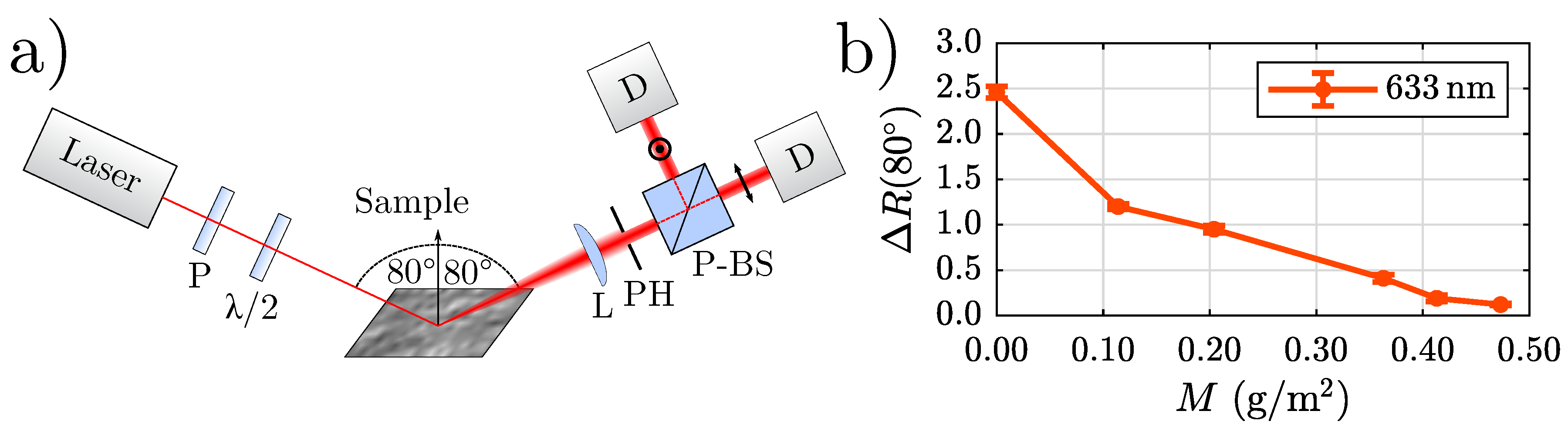
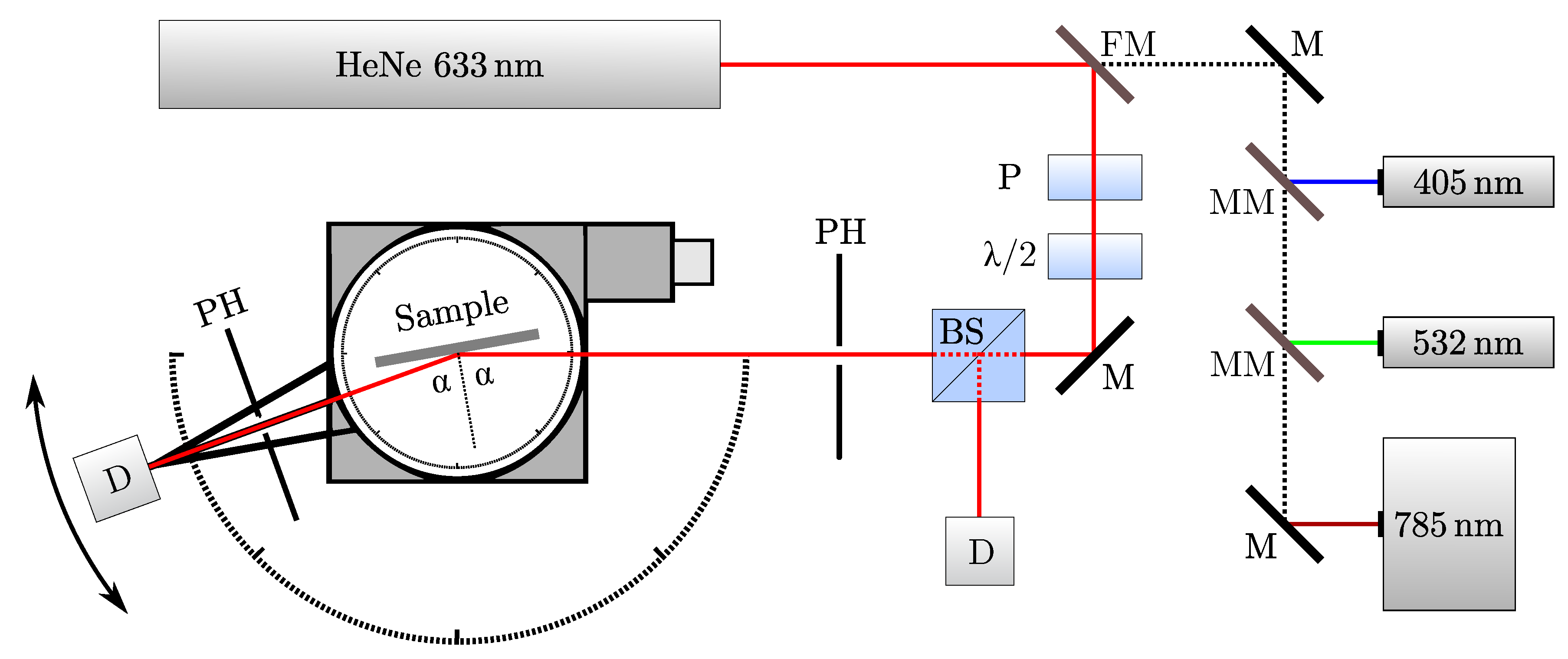
2.2. Methods
3. Experimental Results
3.1. Reference Measurements
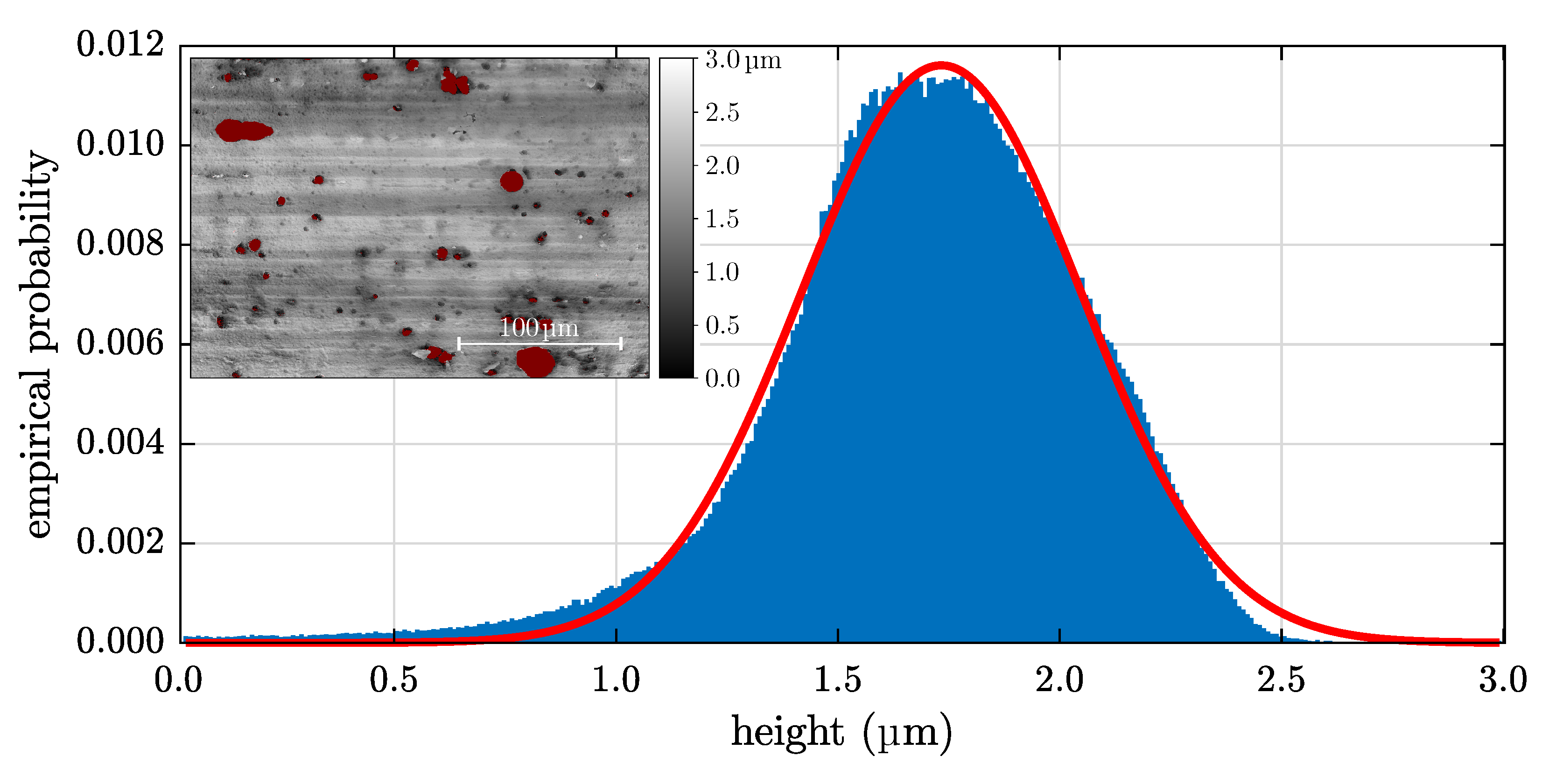
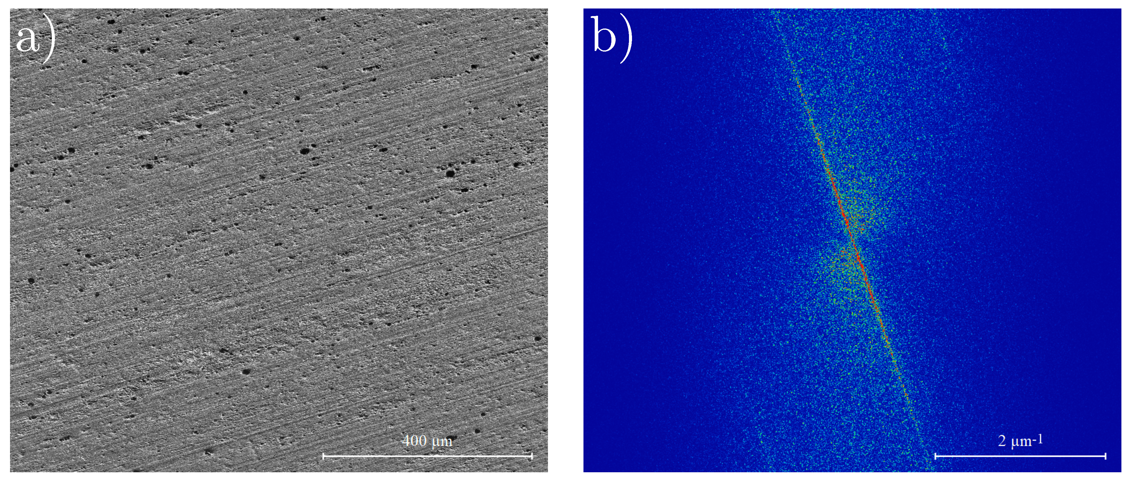
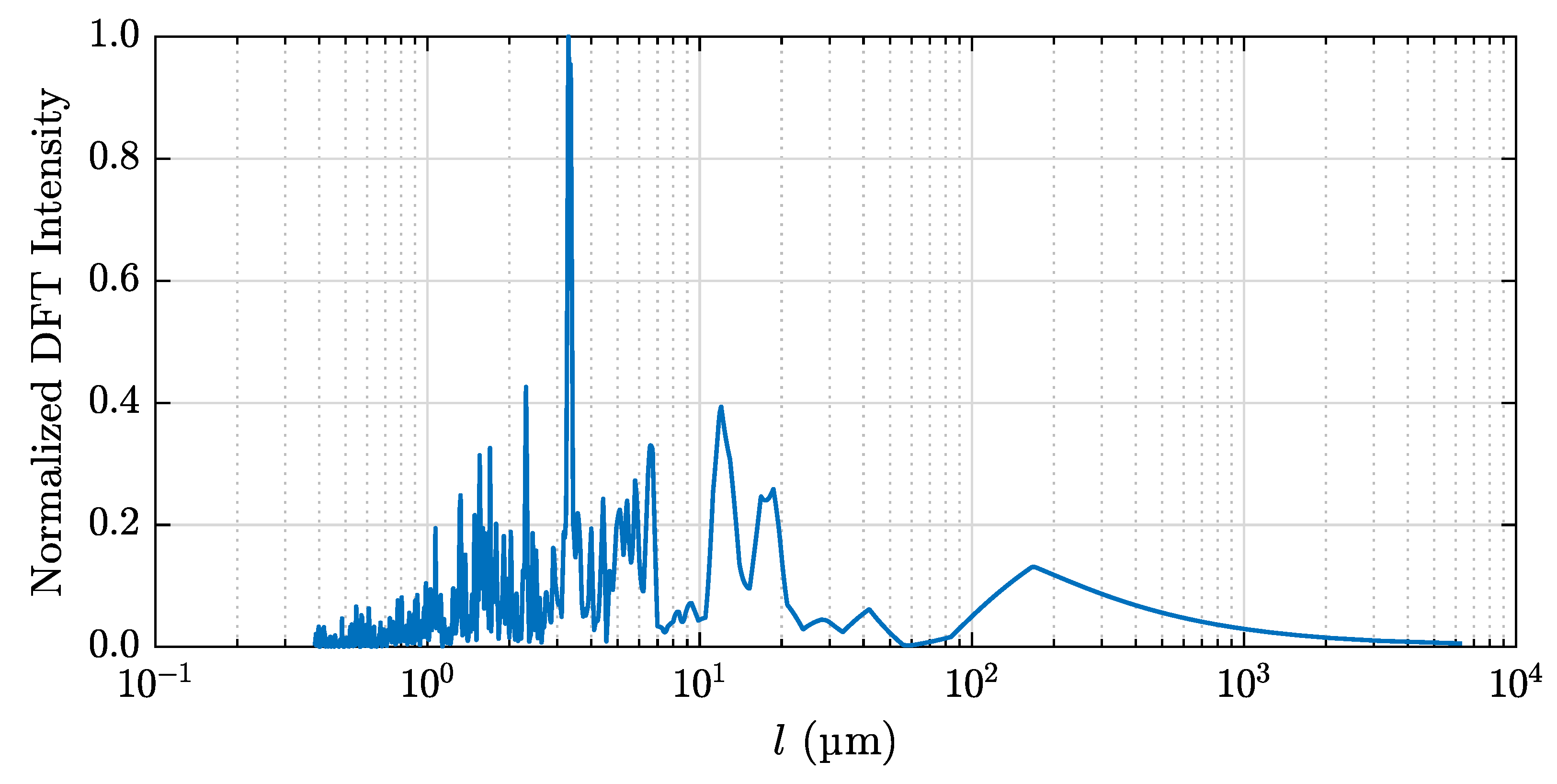
3.1.1. Roughness: LSCM
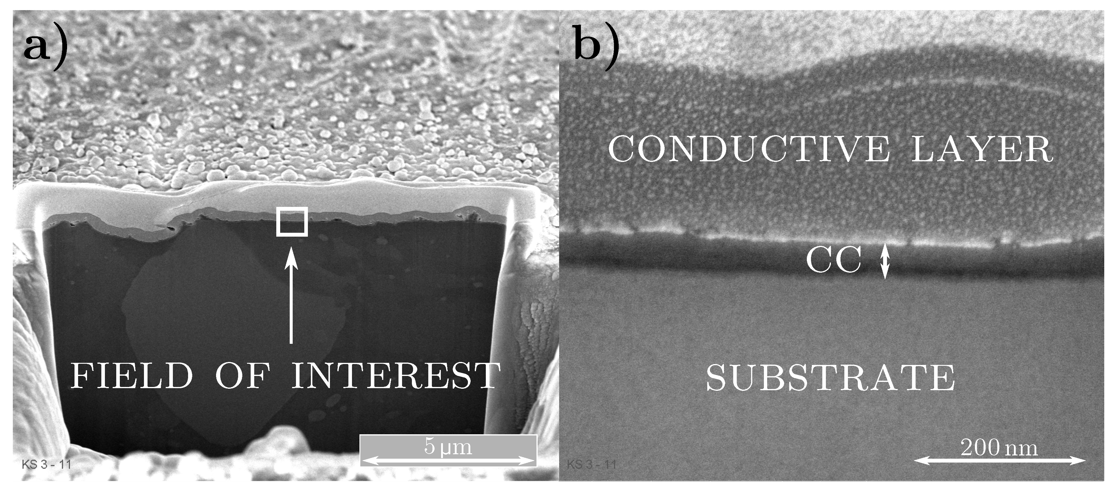
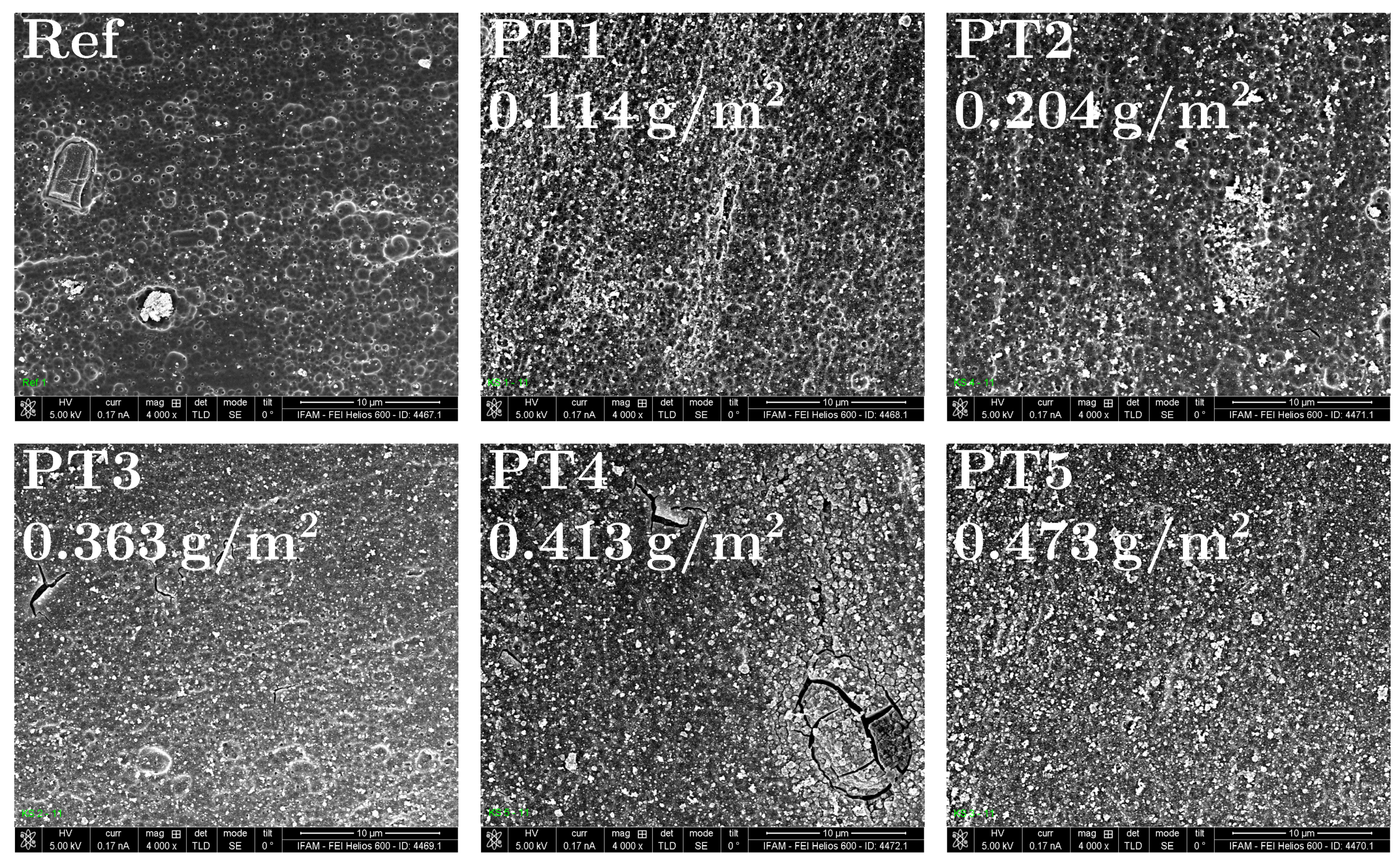
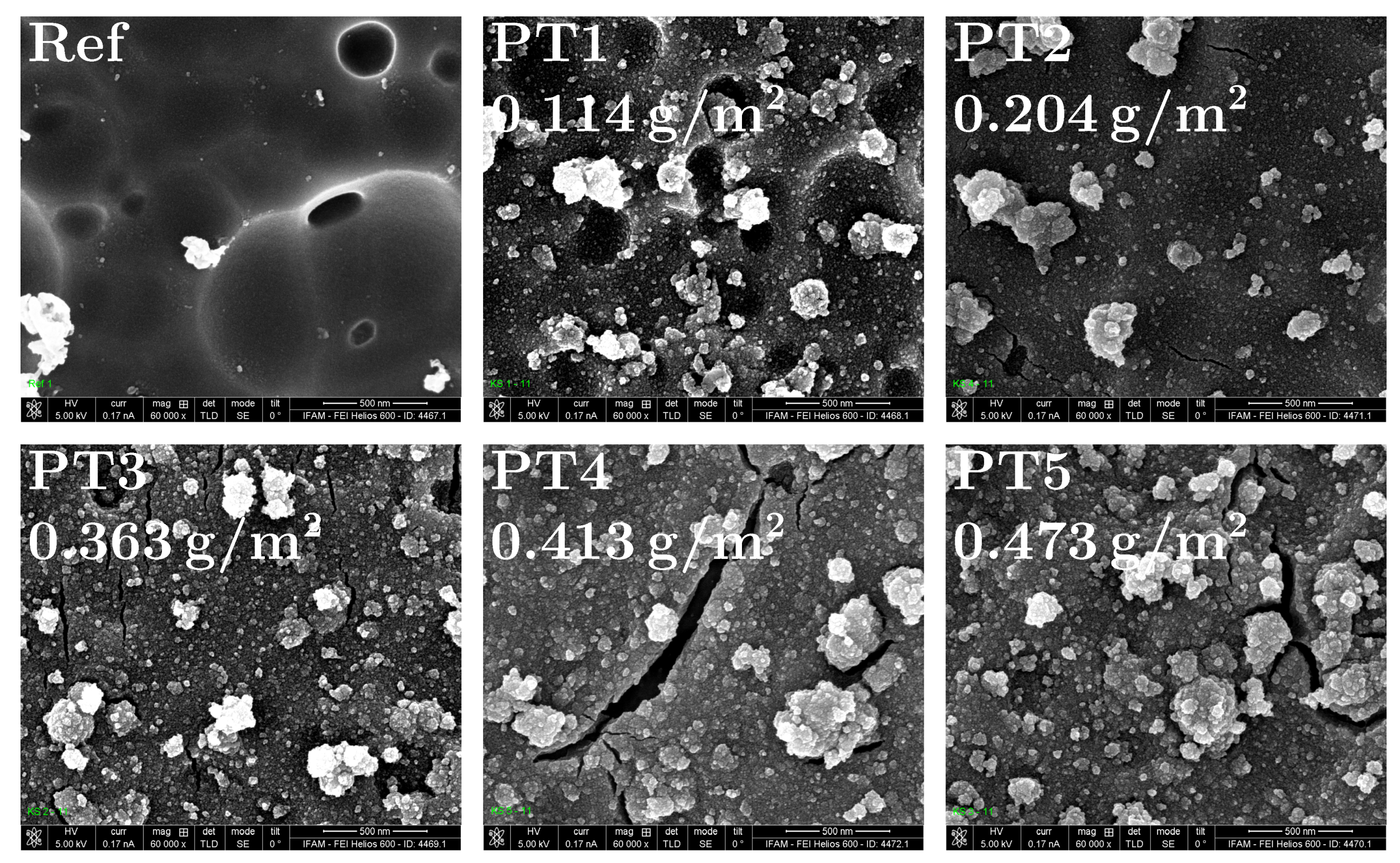
3.1.2. Coating Weight and Thickness: FIB Section
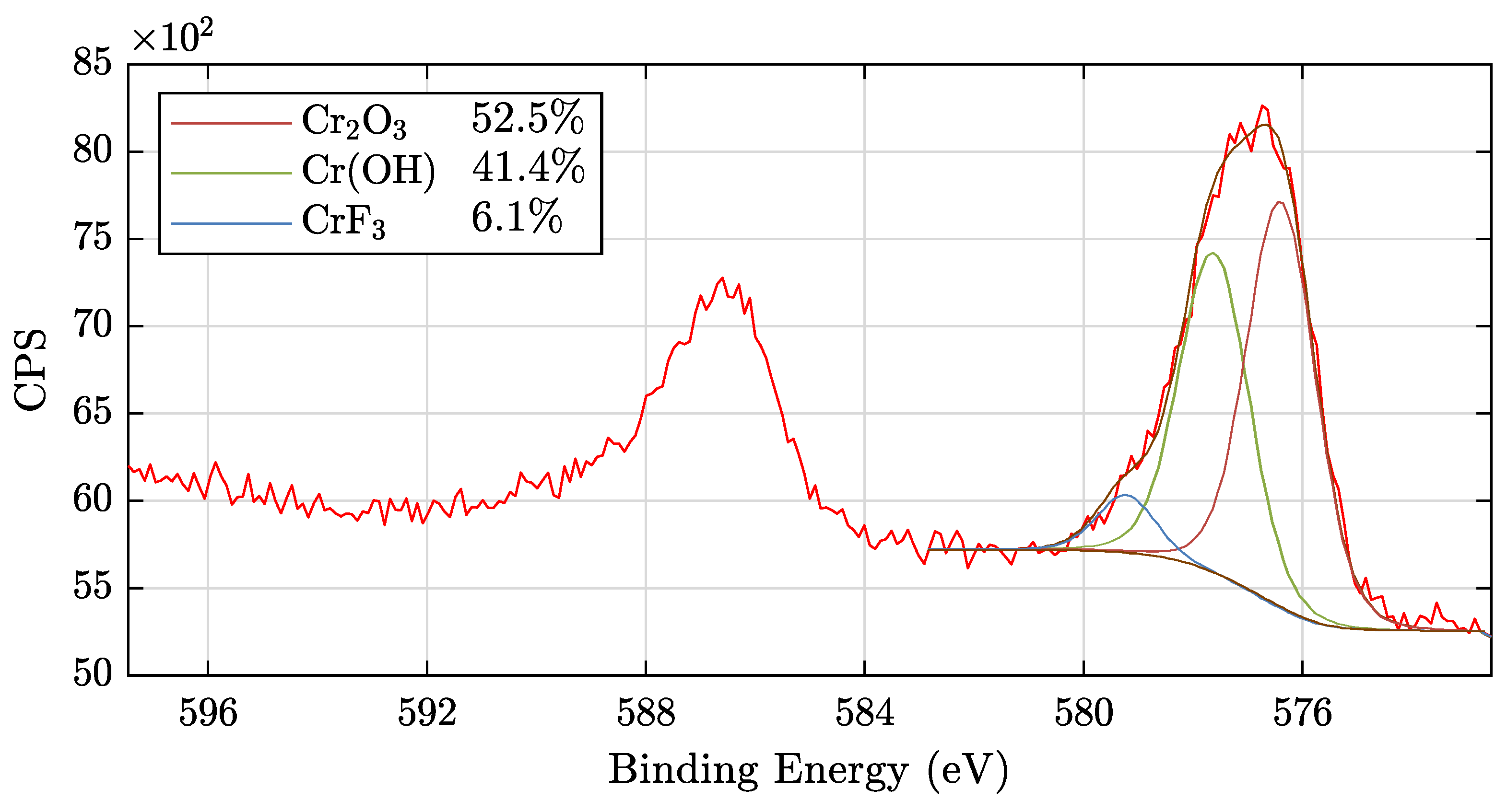
3.1.3. Chemical Composition of the TCC Coatings: XPS
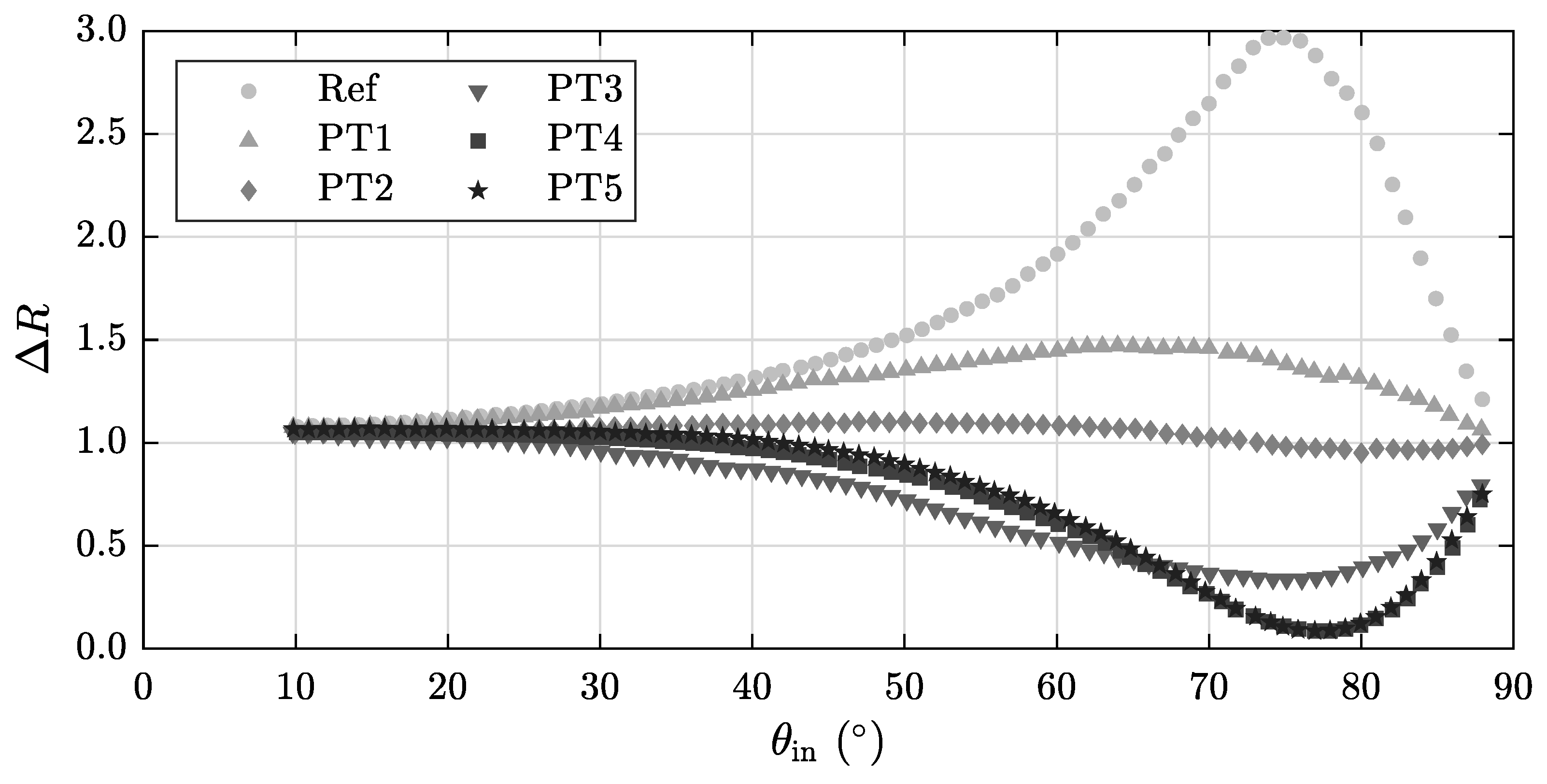
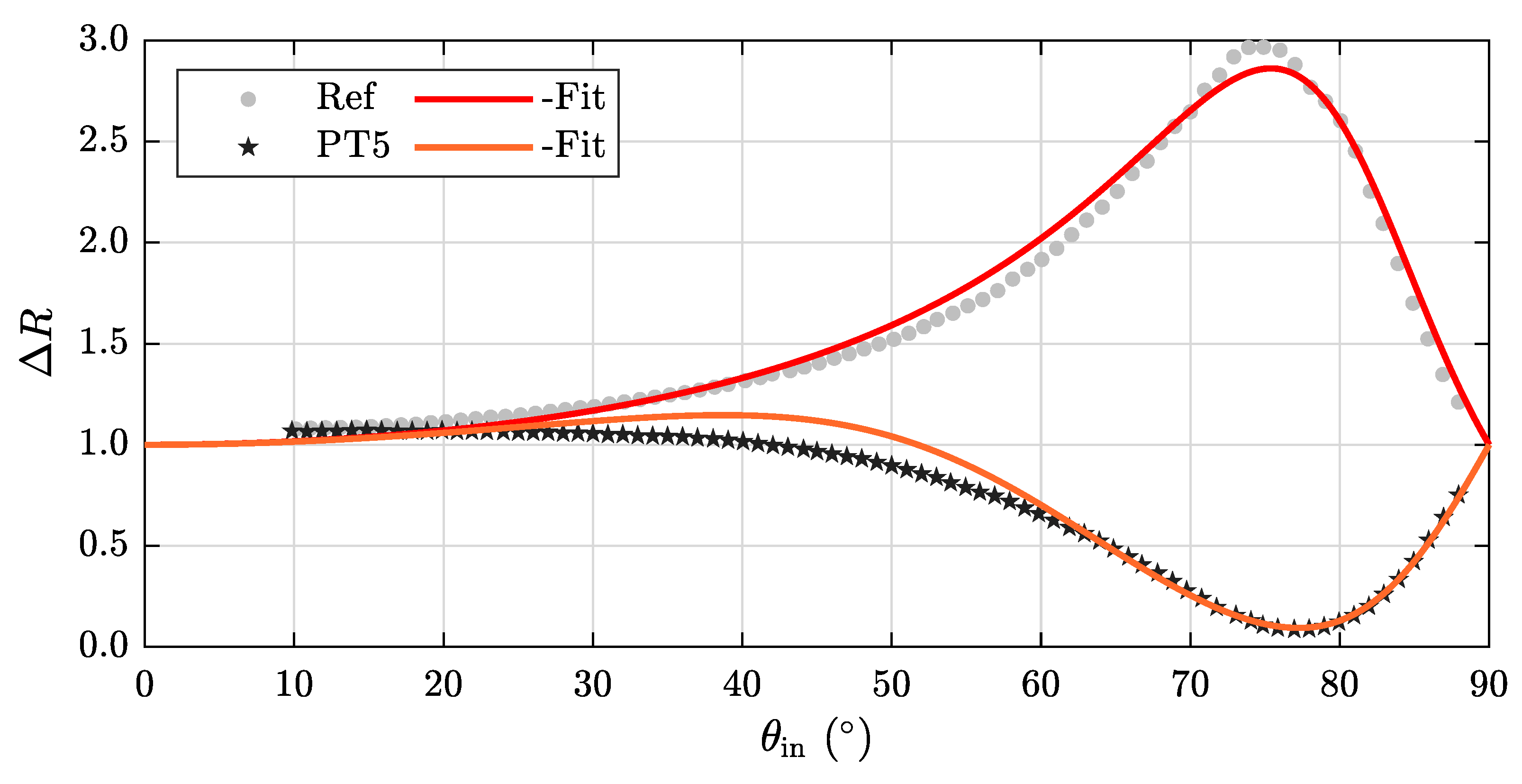
3.2. Optical Measurements
4. Discussion
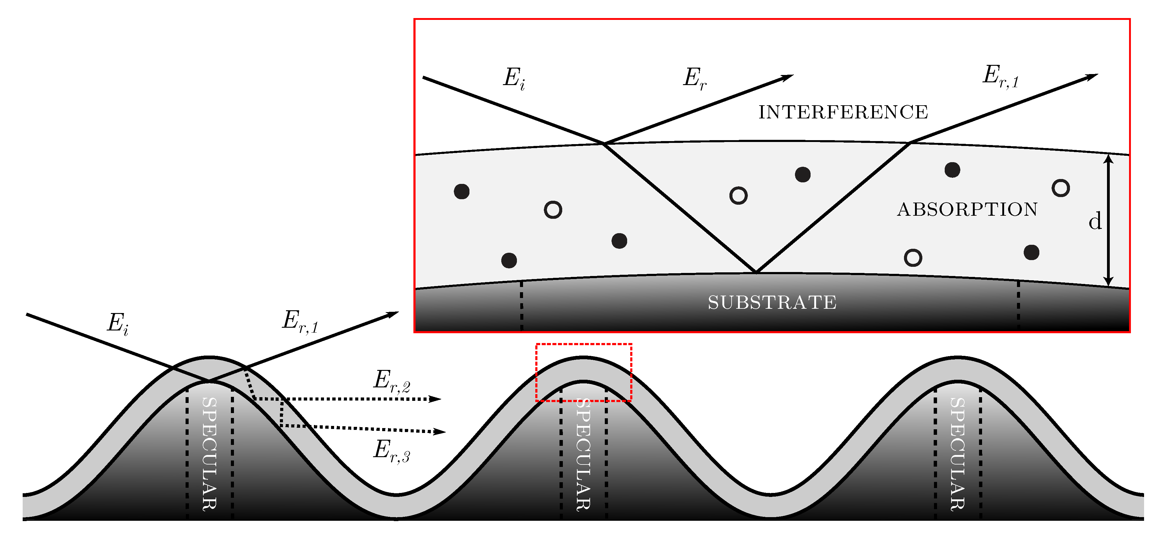
4.1. Three Layer Model for TCC Coatings on Cold-Rolled Aluminium
4.2. Evaluation of the Proposed Model
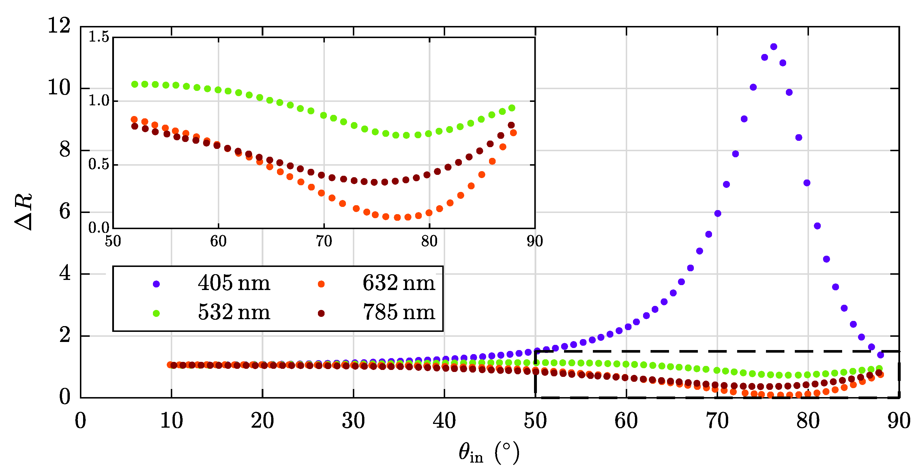
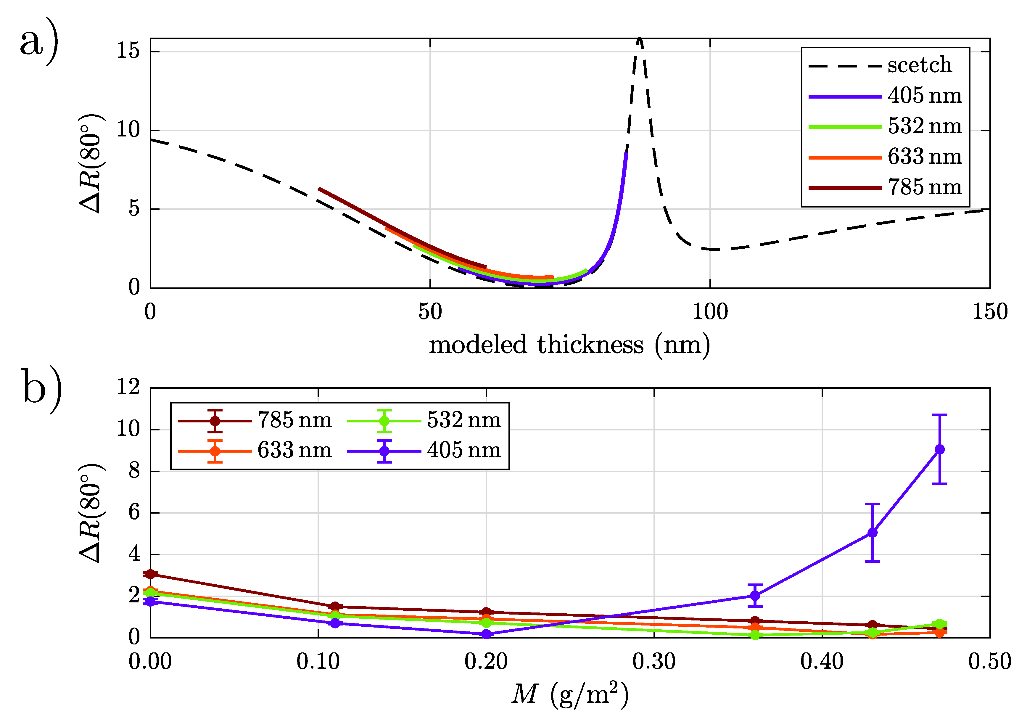
4.3. Determination of the Optimal Wavelength
4.4. Conclusions and Future Work
Supplementary Materials
Author Contributions
Funding
Acknowledgments
Conflicts of Interest
Abbreviations
| AA | aluminium alloy |
| BS | beam splitter |
| CCC | chromate conversion coating |
| D | Si-photodiode |
| FM | flip-mirror |
| L | lens |
| M | mirrors |
| MM | magnetic mirrors |
| P | polarizer |
| P-BS | polarizing beam splitter |
| PH | pinhole |
| PT | pretreatment |
| SE | spectroscopic ellipsometry |
| TCC | trivalent chromium conversion |
| TCP | trivalent chromaium coating |
Appendix A


Appendix B
References
- Becherini, F.; Lucchi, E.; Gandini, A.; Barrasa, M.C.; Troi, A.; Roberti, F.; Sachini, M.; Tuccio, M.C.D.; Arrieta, L.G.; Pockelé, L.; et al. Characterization and thermal performance evaluation of infrared reflective coatings compatible with historic buildings. Build. Environ. 2018, 134, 35–46. [Google Scholar] [CrossRef]
- Tschentscher, J.; Hochheim, S.; Brüning, H.; Brune, K.; Voit, K.M.; Imlau, M. Optical Riblet Sensor: Beam Parameter Requirements for the Probing Laser Source. Sensors 2016, 16, 458. [Google Scholar] [CrossRef] [PubMed]
- Eggert, J.; Bourdon, B.; Nolte, S.; Rischmueller, J.; Imlau, M. Chirp control of femtosecond-pulse scattering from drag-reducing surface-relief gratings. Photonics Res. 2018, 6, 542. [Google Scholar] [CrossRef]
- Helmus, M.N.; Gibbons, D.F.; Cebon, D. Biocompatibility: Meeting a Key Functional Requirement of Next-Generation Medical Devices. Toxicol. Pathol. 2008, 36, 70–80. [Google Scholar] [CrossRef]
- Liu, Z.; Tabakman, S.; Welsher, K.; Dai, H. Carbon nanotubes in biology and medicine: In vitro and in vivo detection, imaging and drug delivery. Nano Res. 2009, 2, 85–120. [Google Scholar] [CrossRef]
- Kendig, M.; Davenport, A.; Isaacs, H. The mechanism of corrosion inhibition by chromate conversion coatings from x-ray absorption near edge spectroscopy (Xanes). Corros. Sci. 1993, 34, 41–49. [Google Scholar] [CrossRef]
- Zhao, J. Corrosion Protection of Untreated AA-2024-T3 in Chloride Solution by a Chromate Conversion Coating Monitored with Raman Spectroscopy. J. Electrochem. Soc. 1998, 145, 2258. [Google Scholar] [CrossRef]
- Qi, J.; Hashimoto, T.; Walton, J.; Zhou, X.; Skeldon, P.; Thompson, G.E. Formation of a Trivalent Chromium Conversion Coating on AA2024-T351 Alloy. J. Electrochem. Soc. 2015, 163, C25–C35. [Google Scholar] [CrossRef]
- Qi, J.T.; Hashimoto, T.; Walton, J.; Zhou, X.; Skeldon, P.; Thompson, G. Trivalent chromium conversion coating formation on aluminium. Surf. Coat. Technol. 2015, 280, 317–329. [Google Scholar] [CrossRef]
- Qi, J.; Walton, J.; Thompson, G.E.; Albu, S.P.; Carr, J. Spectroscopic Studies of Chromium VI Formed in the Trivalent Chromium Conversion Coatings on Aluminum. J. Electrochem. Soc. 2016, 163, C357–C363. [Google Scholar] [CrossRef]
- Qi, J.; Gao, L.; Li, Y.; Wang, Z.; Thompson, G.E.; Skeldon, P. An Optimized Trivalent Chromium Conversion Coating Process for AA2024-T351 Alloy. J. Electrochem. Soc. 2017, 164, C390–C395. [Google Scholar] [CrossRef]
- Qi, J.; Gao, L.; Liu, Y.; Liu, B.; Hashimoto, T.; Wang, Z.; Thompson, G.E. Chromate Formed in a Trivalent Chromium Conversion Coating on Aluminum. J. Electrochem. Soc. 2017, 164, C442–C449. [Google Scholar] [CrossRef]
- Honselmann, J.; Volk, P.; Mankel, E. Analyse der Schichtbildung Chrom(III)-haltiger Aluminium- Passivierungen. Galvanotechnik 2015, 4, 722–729. [Google Scholar]
- Mujdrica Kim, M.; Kapun, B.; Tiringer, U.; Šekularac, G.; Milošev, I. Protection of Aluminum Alloy 3003 in Sodium Chloride and Simulated Acid Rain Solutions by Commercial Conversion Coatings Containing Zr and Cr. Coatings 2019, 9, 563. [Google Scholar] [CrossRef]
- Dardona, S.; Jaworowski, M. In situ spectroscopic ellipsometry studies of trivalent chromium coating on aluminum. Appl. Phys. Lett. 2010, 97, 181908. [Google Scholar] [CrossRef]
- Dardona, S.; Chen, L.; Kryzman, M.; Goberman, D.; Jaworowski, M. Polarization Controlled Kinetics and Composition of Trivalent Chromium Coatings on Aluminum. Anal. Chem. 2011, 83, 6127–6131. [Google Scholar] [CrossRef]
- Lehmann, D.; Seidel, F.; Zahn, D.R. Thin films with high surface roughness: Thickness and dielectric function analysis using spectroscopic ellipsometry. SpringerPlus 2014, 3. [Google Scholar] [CrossRef]
- Siah, S.; Hoex, B.; Aberle, A. Accurate characterization of thin films on rough surfaces by spectroscopic ellipsometry. Thin Solid Film. 2013, 545, 451–457. [Google Scholar] [CrossRef]
- Imlau, M.; Toschke, Y.; Rischmüller, J.; Schlag, M.; Brüning, H.; Brune, K. Vorbehandlungsprüfung mit dem Laserpointer. JOT J. Für Oberflächentechnik 2019, 59, 46–49. [Google Scholar] [CrossRef]
- Davis, J.R. Alloying: Understanding the Basics (06117G); ASM International: Materials Park, OH, USA, 2001. [Google Scholar]
- Silvennoinen, R.; Peiponen, K.E.; Asakura, T.; Zhang, Y.F.; Gu, C.; Ikonen, K.; Morley, E. Specular reflectance of cold-rolled aluminum surfaces. Opt. Lasers Eng. 1992, 17, 103–109. [Google Scholar] [CrossRef]
- Beckmann, P.; Spizzichino, A. The Scattering of Electromagnetic Waves from Rough Surfaces; Artech House: Norwood, MA, USA, 1987. [Google Scholar]
- Hensler, D.H. Light Scattering from Fused Polycrystalline Aluminum Oxide Surfaces. Appl. Opt. 1972, 11, 2522. [Google Scholar] [CrossRef] [PubMed]
- Ragheb, H.; Hancock, E.R. The modified Beckmann–Kirchhoff scattering theory for rough surface analysis. Pattern Recognit. 2007, 40, 2004–2020. [Google Scholar] [CrossRef]


| Processing Step | Function | Product | Concentration (Vol%) | Temperature (C) | Time (min:sec) |
|---|---|---|---|---|---|
| 1 | Cleaning | SurTec® 089 | 60 | 10:00 | |
| Degreasing | SurTec® 061 | ||||
| 2 | Rinsing | Process water | RT | 1:00 | |
| 3 | Rinsing | DI-water | RT | 1:00 | |
| 4 | Alkaline Etching | SurTec® 181 | 50 | 0:30 | |
| 5 | Rinsing | Process water | RT | 1:00 | |
| 6 | Rinsing | DI-water | RT | 1:00 | |
| 7 | Desmutting | SurTec® 496 | 20 | 26 | 5:00 |
| 8 | Rinsing | Process water | RT | 1:00 | |
| 9 | Rinsing | DI-water | RT | 1:00 | |
| 10 | Passivation | SurTec® 650 (SurTec® 650 A) | 20, (5) | Variable | Variable |
| 11 | Rinsing | DI-water | RT | 1:00 | |
| 12 | Drying | Oven | 80 | 10:00 |
| Sample | Temperature (C) | Time (min:sec) | Coating Weight M |
|---|---|---|---|
| Ref | - | - | - |
| PT1 | 30 | 1:00 | |
| PT2 | 40 | 1:00 | |
| PT3 | 30 | 3:00 | |
| PT4 | 40 | 3:00 | |
| PT5 | 30 | 5:00 |
| Parameter | Ref | PT1 | PT2 | PT3 | PT4 | PT5 |
|---|---|---|---|---|---|---|
| () | 0.29 | 0.26 | 0.26 | 0.29 | 0.26 | 0.28 |
| () | 1.60 | 1.42 | 1.57 | 1.67 | 2.38 | 1.54 |
| Sample | C (at%) | O (at%) | F (at%) | Al (at%) | Cu (at%) | Zr (at%) | Cr (at%) | N (at%) | S (at%) |
|---|---|---|---|---|---|---|---|---|---|
| Ref | 24.1 | 45.4 | 2.2 | 27.9 | 0.3 | - | - | - | - |
| PT1 | 43.0 | 37.0 | 5.0 | 2.9 | - | 6.3 | 3.4 | 2.0 | 0.6 |
| PT2 | 42.3 | 38.0 | 4.6 | 1.8 | - | 6.8 | 3.5 | 2.3 | 0.7 |
| PT3 | 39.7 | 36.9 | 7.0 | 2.4 | - | 7.1 | 4.0 | 2.4 | 0.7 |
| PT4 | 41.2 | 37.5 | 6.1 | 2.3 | - | 7.0 | 3.8 | 1.4 | 0.6 |
| PT5 | 40.6 | 37.3 | 6.9 | 3.1 | - | 7.2 | 3.4 | 1.1 | 0.5 |
| Parameter | PT1 | PT2 | PT3 | PT4 | PT5 |
|---|---|---|---|---|---|
| 0 | |||||
| d (nm) |
© 2020 by the authors. Licensee MDPI, Basel, Switzerland. This article is an open access article distributed under the terms and conditions of the Creative Commons Attribution (CC BY) license (http://creativecommons.org/licenses/by/4.0/).
Share and Cite
Rischmueller, J.; Toschke, Y.; Imlau, M.; Schlag, M.; Brüning, H.; Brune, K. Inspection of Trivalent Chromium Conversion Coatings Using Laser Light: The Unexpected Role of Interference on Cold-Rolled Aluminium. Sensors 2020, 20, 2164. https://doi.org/10.3390/s20082164
Rischmueller J, Toschke Y, Imlau M, Schlag M, Brüning H, Brune K. Inspection of Trivalent Chromium Conversion Coatings Using Laser Light: The Unexpected Role of Interference on Cold-Rolled Aluminium. Sensors. 2020; 20(8):2164. https://doi.org/10.3390/s20082164
Chicago/Turabian StyleRischmueller, Joerg, Yannic Toschke, Mirco Imlau, Mareike Schlag, Hauke Brüning, and Kai Brune. 2020. "Inspection of Trivalent Chromium Conversion Coatings Using Laser Light: The Unexpected Role of Interference on Cold-Rolled Aluminium" Sensors 20, no. 8: 2164. https://doi.org/10.3390/s20082164
APA StyleRischmueller, J., Toschke, Y., Imlau, M., Schlag, M., Brüning, H., & Brune, K. (2020). Inspection of Trivalent Chromium Conversion Coatings Using Laser Light: The Unexpected Role of Interference on Cold-Rolled Aluminium. Sensors, 20(8), 2164. https://doi.org/10.3390/s20082164