Design of Surface Enhanced Raman Scattering (SERS) Nanosensor Array


Abstract
1. Introduction
1.1. The Need for Real-Time Monitoring of a Chemical Reaction
1.2. pH Determination and Raman Spectroscopy
2. Principles and Formalism
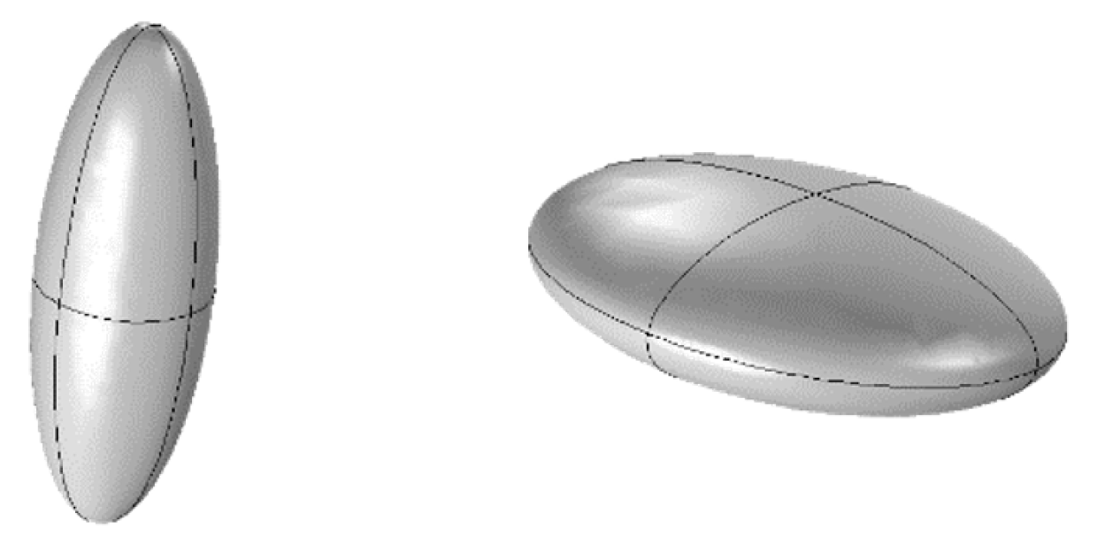
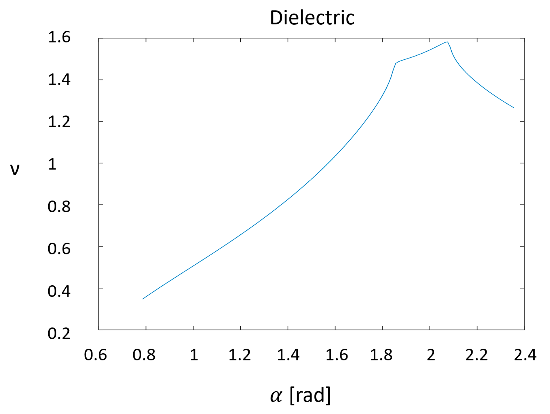
2.1. Case of the Ellipsoid
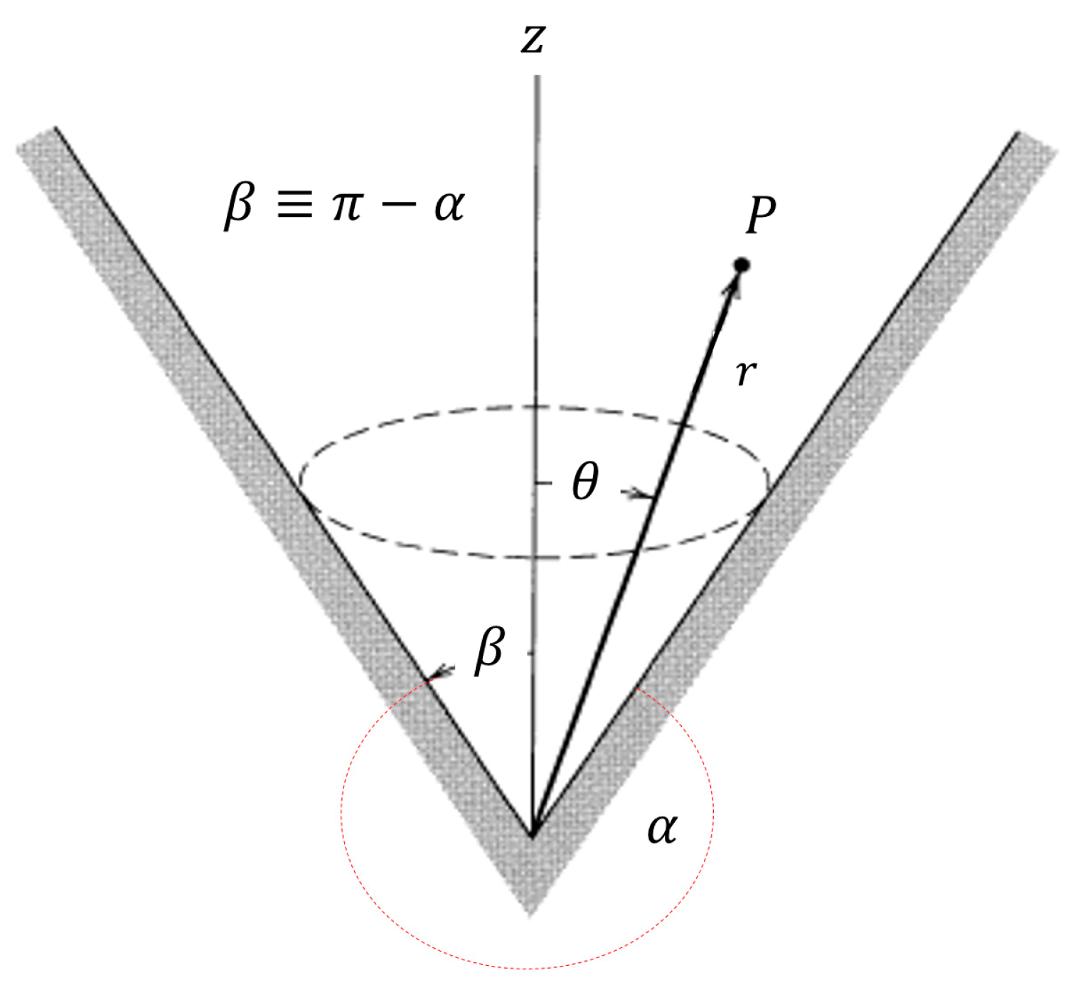
2.2. Nano-Cones
2.3. Nanoshells
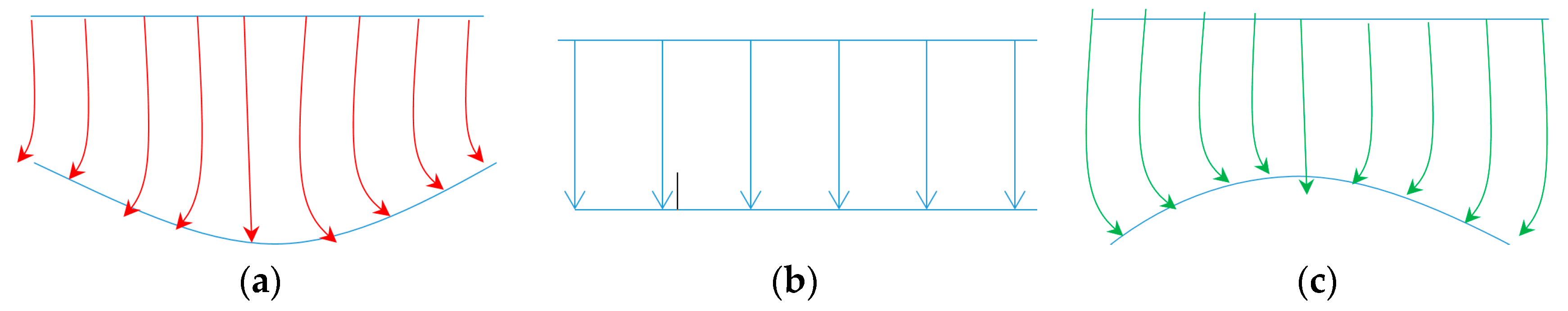
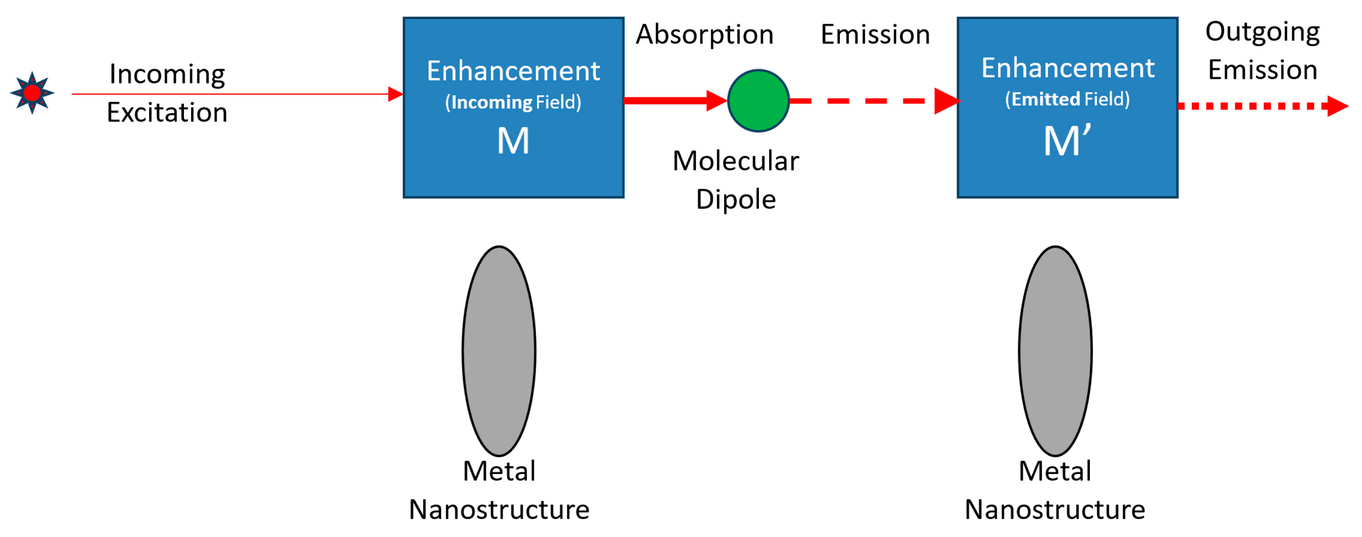
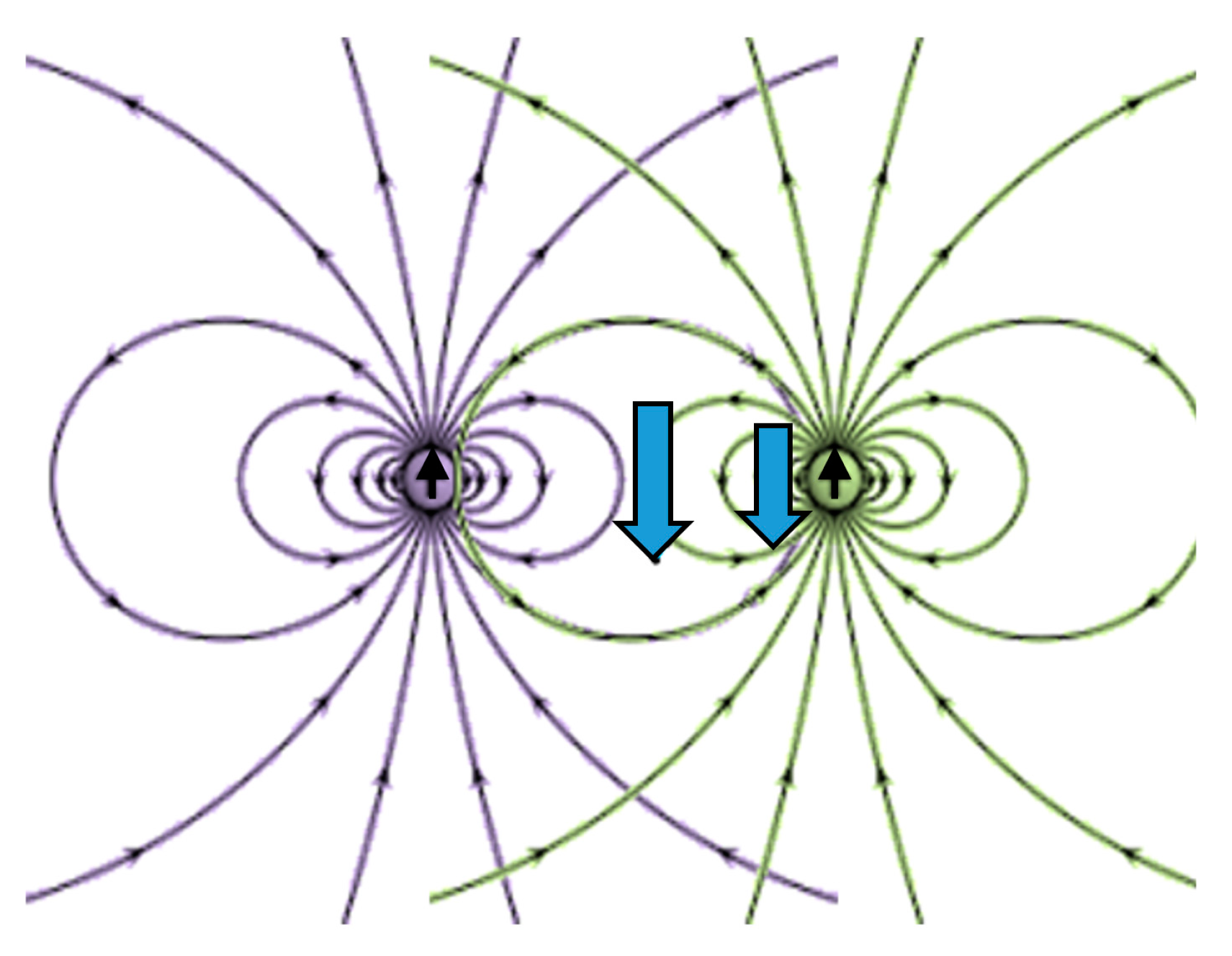
2.4. Multiple Nanostructures
2.4.1. Multiple Nanostructures Influence
2.4.2. Total Raman Emission Cross-Section
3. SERS Biochemical Optical Nanosensors Array
3.1. On-the-Chip pH Raman Imager
3.2. Enhancement Structures
- δdiel is the spacing for which it is possible to sense other plasmons: approximately 250 to 1000 nm,
- δmetal is the penetration depth of the electrical field inside the metal: approximately 5 nm,
- δSPP is the distance where the electrical field extends along the metal: approximately 2–20 µm for λ = 500 nm.
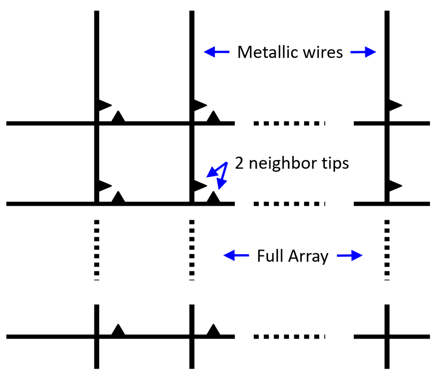
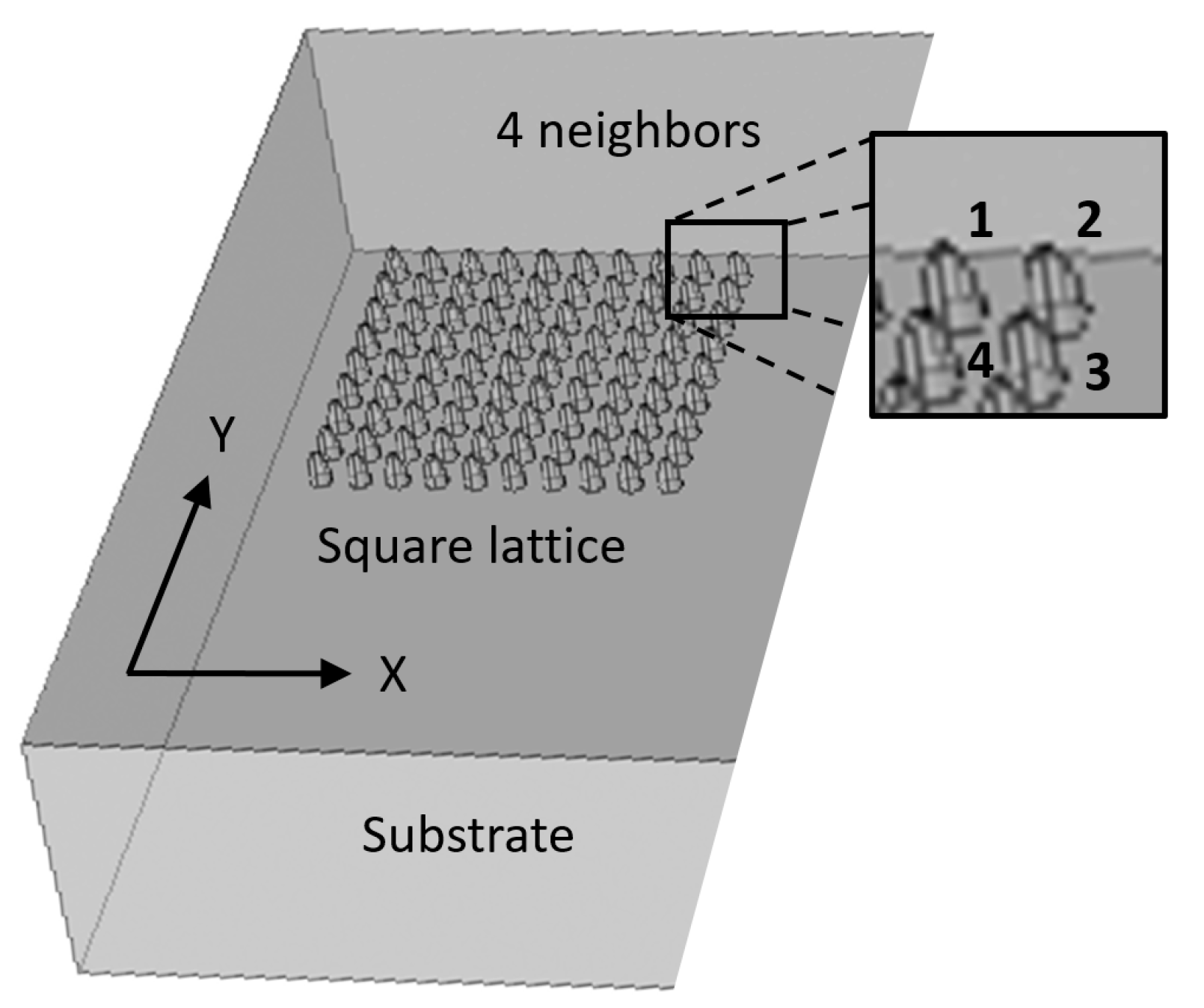
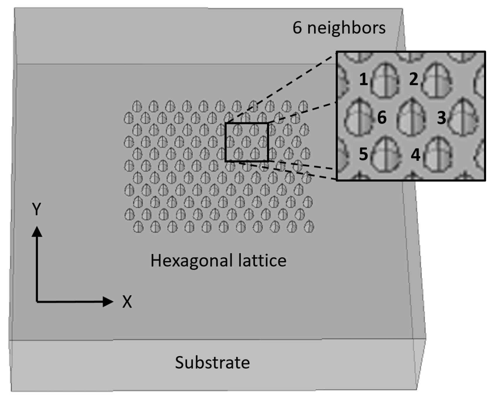
3.3. Square and Hexagonal Lattices
4. Methods: Analytical, Numerical, and Experimental
4.1. Combining Analytical and Numerical
- Field Intensity Enhancement Factors
- Optical Reciprocity Theorem (ORT) and Plane Wave Excitation (PWE)
- Electrostatic Approximation (ESA)
- Image Dipole and Self-Reaction Field
- Generalized Mie Theory
- Spheroids and Prolate Spheroidal Coordinates: Helmoltz Equation
- E4 Approximation, used and presented in this article
4.2. Comsol Multi-Physics: Concerns and Considerations
4.3. Fabrication Methods
- Sample Preparation—Previous to the FIB steps, it was necessary to prepare the substrate to serve as an adequate sample. One initial suggestion was to use a dielectric substrate made of a glass microscope slide to be coated with silver using a vapor deposition process. Since such slides are not particularly smooth on the nanoscale, the question was raised regarding to what extent will this affect the smoothness of the surface of the silver layer and hence the variability in the height of the nanostructures. This is why the alternative of using quality silicon wafer was necessary. Moreover, the cleaning procedure of silicon is much easier and standard than that of glass.
- FIB Accuracy—Two types of equipment were available: One FIB, using a Gallium (Ga) beam, shares a resolution down to 13 nm, but in practice, it is more recommended for structures and separations above approximately 100 nm. Another FIB, using a Helium (He) beam, shares lighter particles; hence, it is easier to focus, and a greater resolution is available. Looking for high resolution, the He FIB was preferable; however, looking at the trade-off of the longer run time, Ga FIB was chosen. In order to assure a smooth move from design to FIB fabrication, STL files, which are fully compatible with the FIB operating software, were prepared with the layout of the pixels. In such a way, the design accuracy was respected.
- Pixel Separation—In order to resolve the signal from separate signals using a Raman microscope—remote imaging using a lens—the pixels must be separated by about 6 to 10 microns. For later designs using near field collection, this may not be necessary, which could be important, as discussed in the next item.
- Large-Scale Lithography—In addition to the resolution, the current design presents another challenge to FIB design: pixel separation. Since a flat metal sheet also provides Raman enhancement, the region between pixels could cause crosstalk. Thus, the metal layer in this ‘no-man’s land’ ought to be removed. Milling several microns width of the silver down to the dielectric substrate would likely prove-time consuming for the FIB, especially if several pixels are concerned.
- Lithography—Looking at the long-term industrial processing of several hundred pixels to be easily produced this way, the lithography process (masks, etching, etc…) was also considered. However, there is some understanding that rounded and pointed structures are an issue for the layer-by-layer methodology underlying lithography.
- Surface Functionalization—Following fabrication, a chemical process of surface functionalization is necessary. Surface activation is usually necessary to purify the surface of contaminants. However, surface activation is not necessary after vapor deposition and FIB milling if the specimen is immediately exposed to the functionalization treatment. Regarding the process itself, an overnight soak may be sufficient, but it may be more involved. The possibility of applying a Longmuir–Blodgett technique: the pMBA floats on the surface of a solution, after which the specimen is dipped vertically and methodically extracted. Surface tension causes the adhesion of a monolayer.
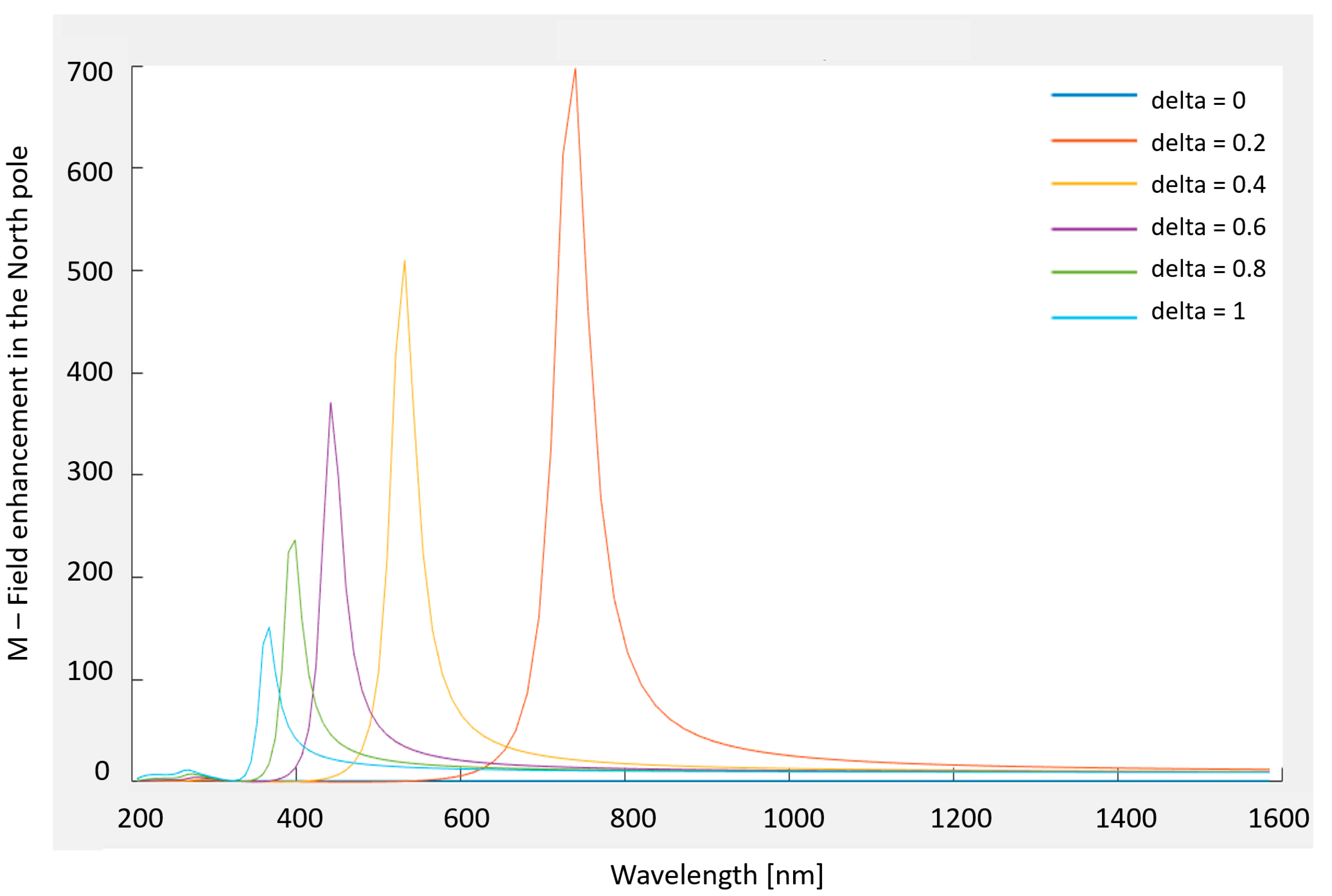
- Optimal Aspect Ratio—Homellhoff’s article [32] mentions that for an ellipsoidal nanostructure, for any given wavelength, there is an optimal aspect ratio, and not just the other way around (a resonant wavelength for a given aspect ratio). Thus, in order get the best performance from the design that is submitted to the FIB, it would be helpful to decide in advance what wavelength will be used.
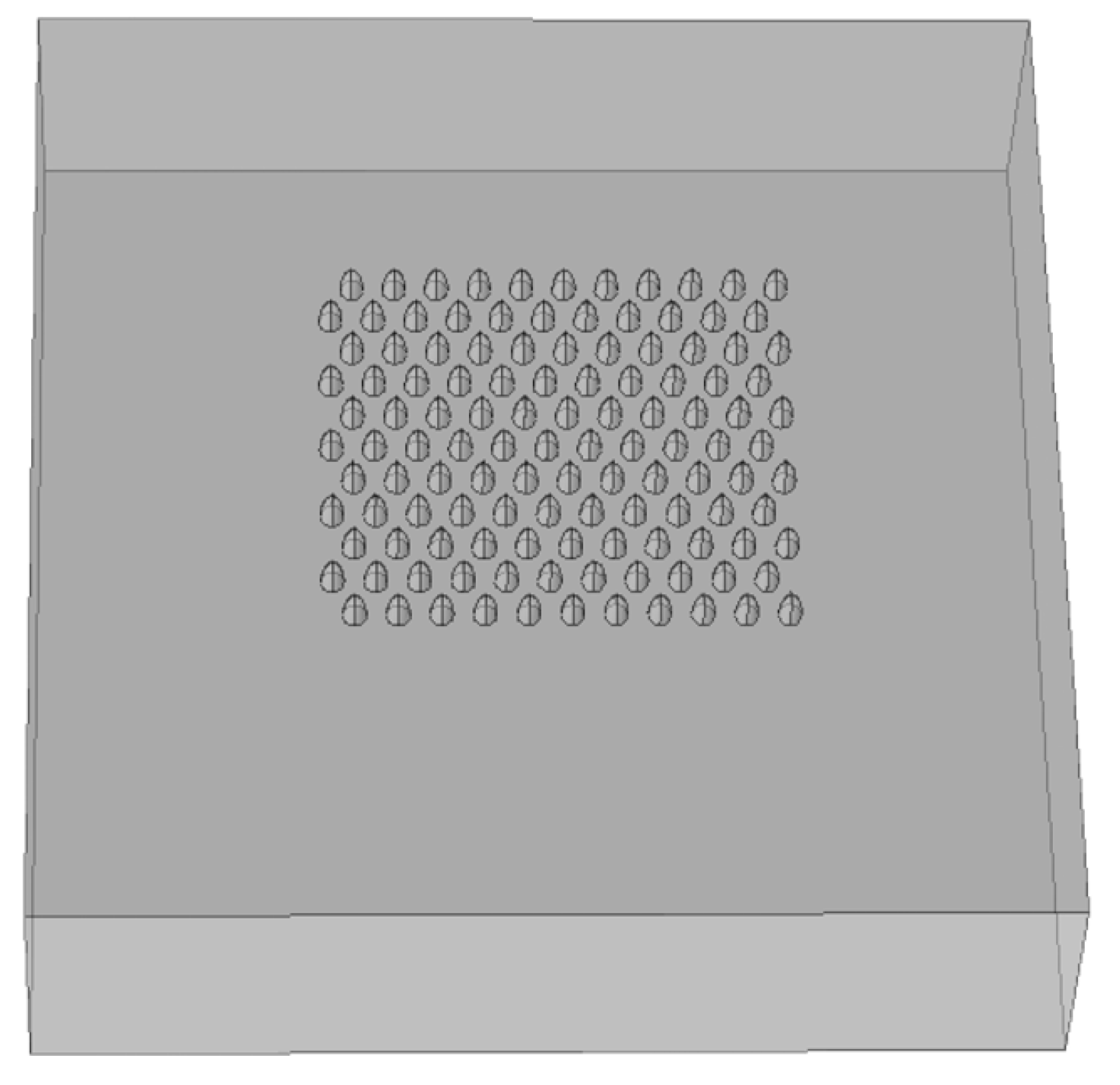
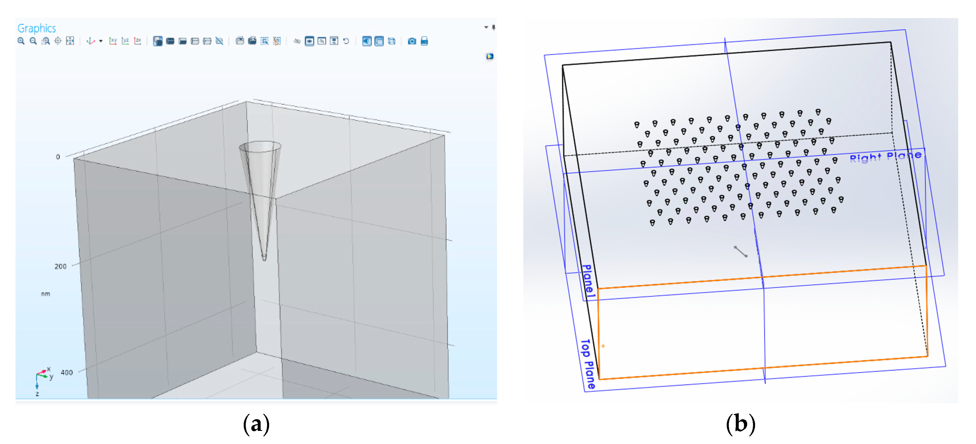
- Executive Summary—The Ga FIB is the appropriate machine. Inserting the dielectric function of silver will give the optimal aspect ratio. Doing the same for gold and comparing the predicted enhancement will help decide which material to use. Using the results to create new STL or BMP files, which are compatible formats for the FIB processing, will enable a smooth move from design to fabrication. The simulations included arrays of nanocavities (Figure 14). The whole fabrication process ensured maximally sterile conditions.
5. Experimental Results
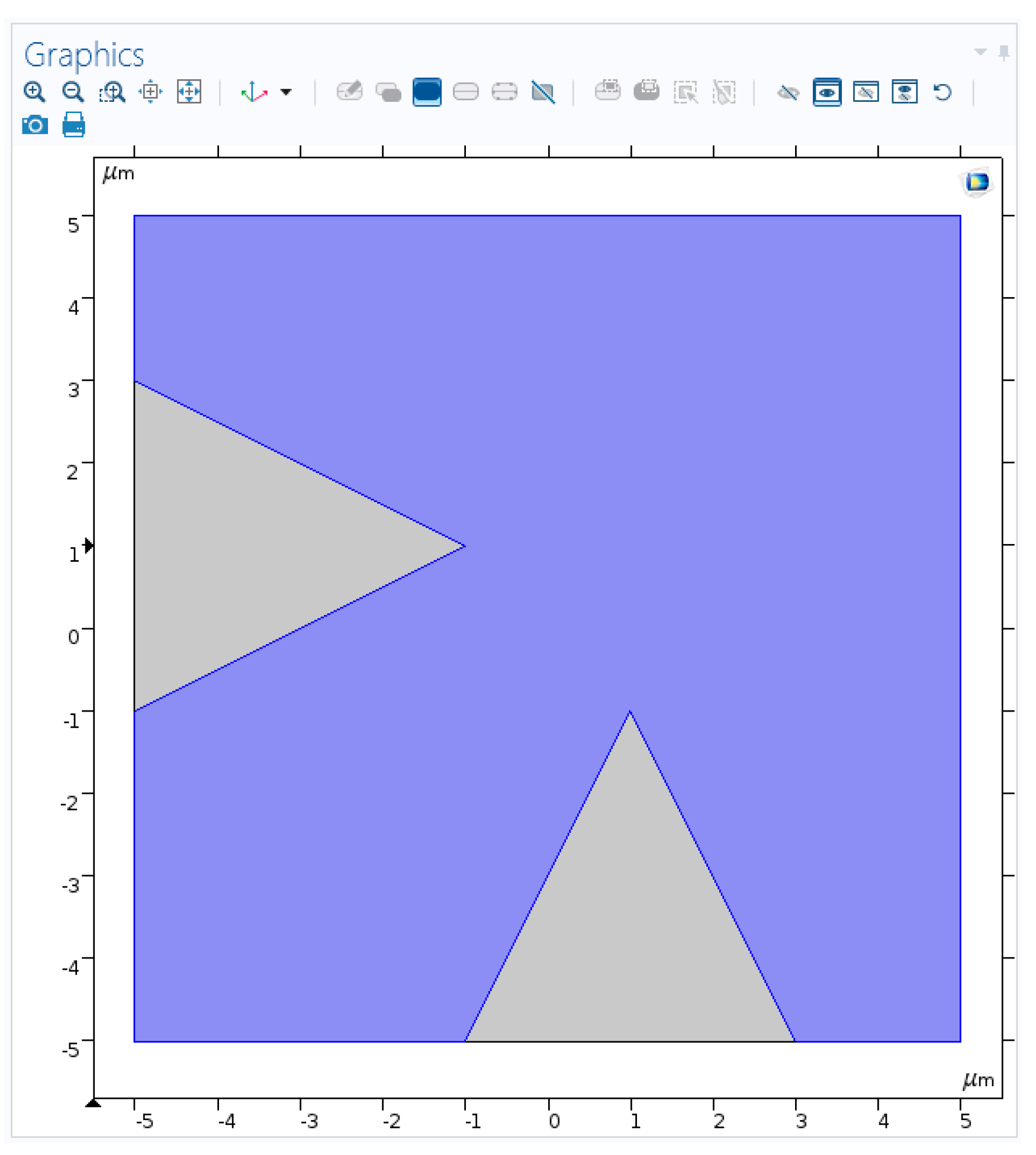
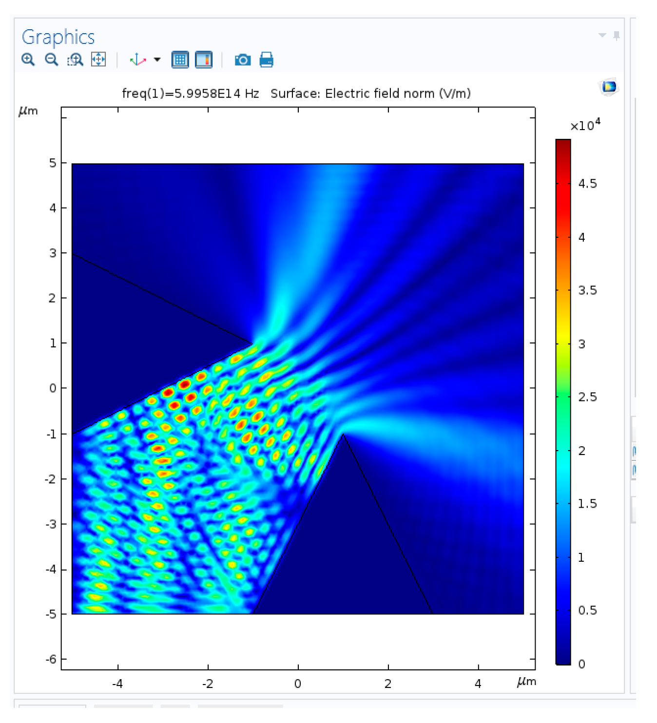
5.1. Simulation Results: Nanocones, Nanoholes, and SERS Pixels Full Array
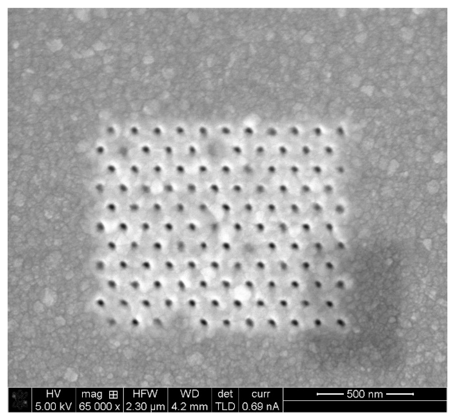
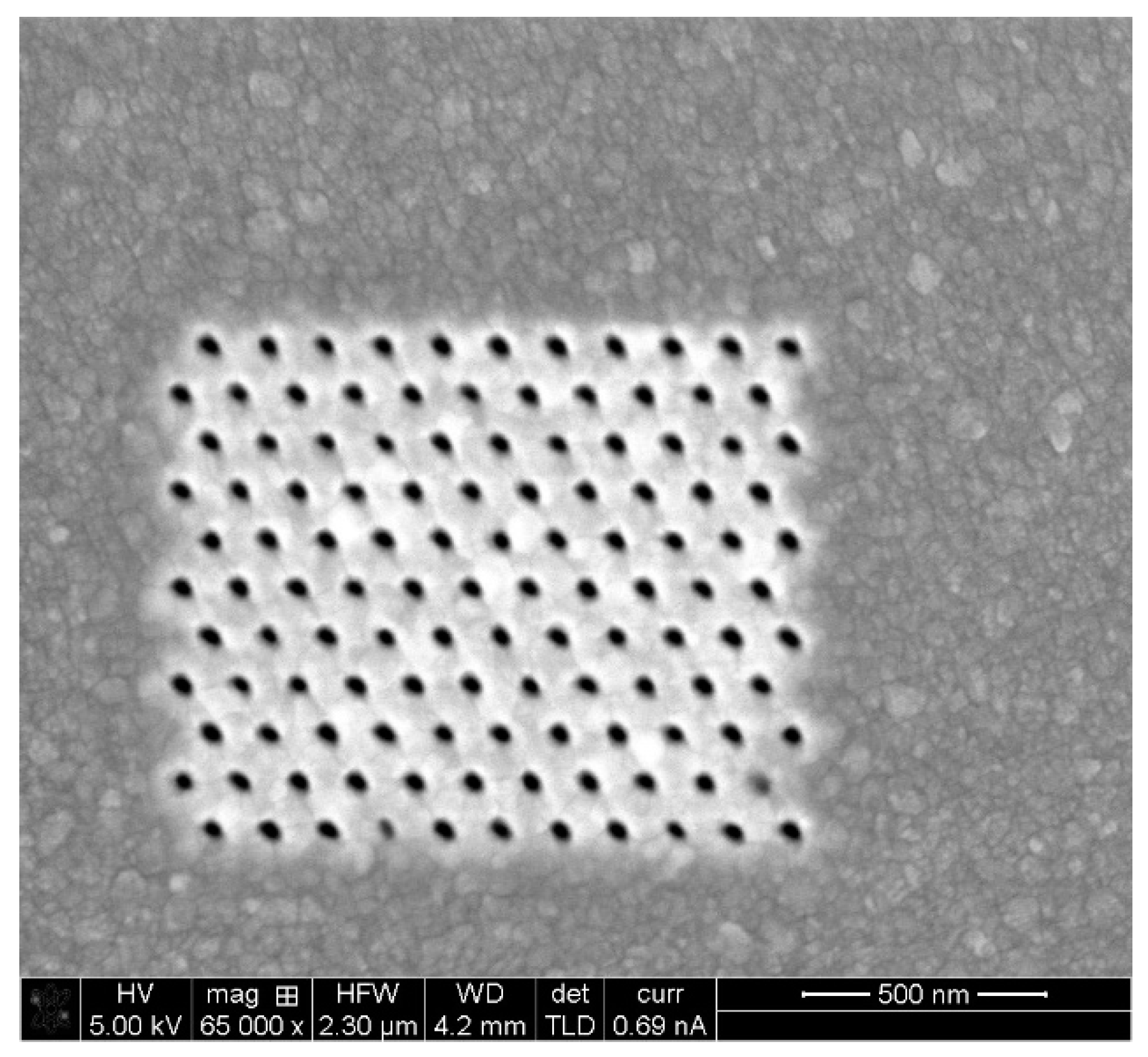
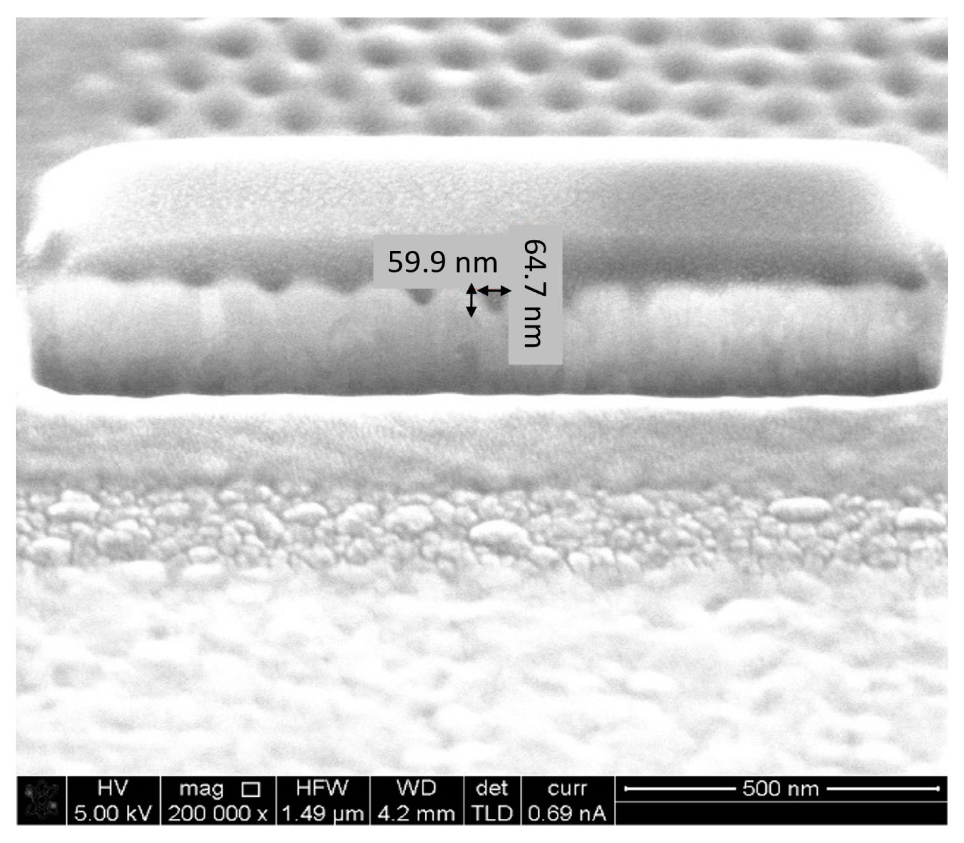
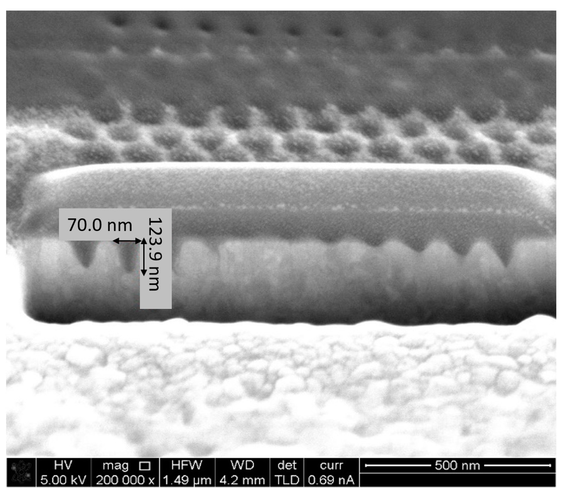
5.2. Fabrication and Structural Charcaterization Results
5.3. Techniques Survey of Optical Measurements, Detection, and Collection
5.4. Preferred Technique: Saddle Point Integration Method for Spatial Coordinate Transformation
6. Conclusions
Author Contributions
Funding
Acknowledgments
Conflicts of Interest
References
- Etchegoin, P.; LeRu, E. Principles of Surface Enhanced Raman Spectroscopy; Elsevier: Amsterdam, The Netherlands, 2009. [Google Scholar]
- Opilik, L.; Schmid, T.; Zenobi, R. Modern Raman Imaging: Vibrational Spectroscopy on the Micrometer and Nanometer Scales. Ann. Rev. Anal. Chem. 2013, 6, 379–398. [Google Scholar] [CrossRef] [PubMed]
- Andreou, C.; Mirsafavi, R.; Moskovits, M.; Meinhart, C.D. Detection of low concentrations of ampicillin in milk. Analyst 2015, 140, 5003–5005. [Google Scholar] [CrossRef] [PubMed]
- Deng, Y.; Juang, Y. Black silicon SERS substrate: Effect of surface morphology on SERS detection and application of single algal cell analysis. Biosens. Bioelectron. 2014, 53, 37–42. [Google Scholar] [CrossRef]
- Sharma, B.; Frontiera, R.R.; Henry, A.-I.; Ringe, E.; Van Duyne, R.P. SERS: Materials, applications, and the future. materialstoday 2012, 15, 16–25. [Google Scholar] [CrossRef]
- Wackerbarth, H.; Salb, C.; Gundrum, L.; Niederkrüger, M.; Christou, K.; Beushausen, V.; Viöl, W. Detection of explosives based on surface-enhanced Raman spectroscopy. Appl. Opt. 2010, 49, 4362–4366. [Google Scholar] [CrossRef]
- Xu, Z.; Jiang, J.; Wang, X.; Han, K.; Ameen, A.; Khan, I.; Chang, T.-W.; Liu, L. Large-area, uniform and low-cost dual-mode plasmonic naked-eye colorimetry and SERS sensor with handheld Raman spectrometer. Nanoscale 2016, 8, 6162–6172. [Google Scholar] [CrossRef]
- Cortés, E.; Etchegoin, P.G.; Le Ru, E.C.; Fainstein, A.; Vela, M.E.; Salvarezza, R.C. Monitoring the Electrochemistry of Single Molecules by Surface-Enhanced Raman Spectroscopy. J. Am. Chem. Soc. 2010, 132, 18034–18037. [Google Scholar] [CrossRef]
- Stewart, S.; Priore, R.J.; Nelson, M.P.; Treado, P.J. Raman Imaging. Annu. Rev. Anal. Chem. 2012, 5, 337–360. [Google Scholar] [CrossRef]
- Alvarez-Puebla, R.A.; Liz-Marza, L.M. Traps and cages for universal SERS detection. Chem. Soc. 2012, 41, 43–51. [Google Scholar] [CrossRef]
- Bishnoi, S.W.; Rozell, C.J.; Levin, C.S.; Gheith, M.K.; Johnson, B.R.; Johnson, D.H.; Halas, N.J. All-Optical Nanoscale pH Meter. NanoLetters 2006, 6, 1687–1692. [Google Scholar] [CrossRef]
- Talley, C.E.; Jusinski, L.; Hollars, C.W.; Lane, S.M.; Huser, T. Intracellular pH Sensors Based on Surface-Enhanced Raman Scattering. Anal. Chem. 2004, 76, 7064–7068. [Google Scholar] [CrossRef]
- Kneipp, J.; Kneipp, H.; Wittig, B.; Kneipp, K. One- and Two-Photon Excited Optical pH Probing for Cells Using Surface-Enhanced Raman and Hyper-Raman Nanosensors. Nano Lett. 2007, 7, 2819–2823. [Google Scholar] [CrossRef] [PubMed]
- Vo-Dinh, T.; Liu, Y.; Fales, A.M.; Ngo, H.; Wang, H.-N.; Register, J.K.; Yuan, H.; Norton, S.J.; Griffin, G.D. SERS Nanosensors and Nanoreporters: Golden Opportunities in Biomedical Applications. Wires Nanomed. Nanobiotechnol. 2015, 7, 17–33. [Google Scholar] [CrossRef] [PubMed]
- Zhao, X.; Campbell, S.; Wallace, G.Q.; Claing, A.; Bazuin, C.G.; Masson, J.-F. Branched Au Nanoparticles on Nanofibers for Surface-Enhanced Raman Scattering Sensing of Intracellular pH and Extracellular pH Gradients. ACS Sens. 2020, 5, 2155–2167. [Google Scholar] [CrossRef] [PubMed]
- Park, J.E.; Yonet-Tanyeri, N.; Ende, E.V.; Henry, A.-I.; Perez White, B.E.; Mrksich, M.; Van Duyne, R.P. Plasmonic Microneedle Arrays for in Situ Sensing with Surface-Enhanced Raman Spectroscopy (SERS). Nano Lett. 2019, 19, 6862–6868. [Google Scholar] [CrossRef] [PubMed]
- Liao, P.; Wokaun, A. Lightning rod effect in surface enhanced Raman scattering. J. Chern. Phys. 1982, 76, 751–752. [Google Scholar] [CrossRef]
- Jackson, J. Classical Electrodynamics, 3rd ed.; Wiley: Hoboken, NJ, USA, 2001. [Google Scholar]
- Landau, L.; Lifshitz, E. Electrodynamics of Continuous Media; Pergamon Press: Bristol, UK, 1960; Volume 8. [Google Scholar]
- Hall, R. The Application of Non-Integral Legendre Functions to Potential Problems. J. Appl. Phys. 1949, 20, 925–931. [Google Scholar] [CrossRef]
- Goncharenko, A.V.; Chang, H.C.; Wang, J.K. Electric near-field enhancing properties of a finite-size metal conical nano-tip. Ultramicroscopy 2007, 107, 151–157. [Google Scholar] [CrossRef]
- Novotny, L.; Hecht, B. Principles of Nano-Optics, 2nd ed.; Cambridge University Press: Cambridge, UK, 2012. [Google Scholar]
- Halas, N. Playing with Plasmons: Tuning the Optical Resonant Properties of Metallic Nanoshells. Mrs Bull. 2005, 30, 362–367. [Google Scholar] [CrossRef]
- Genc, A.; Patarroyo, J.; Sancho-Parramon, J.; Bastus, N.G.; Puntes, V.; Arbiol, J. Hollow metal nanostructures for enhanced plasmonics: Synthesis, local plasmonic properties and applications. Nanophotonics 2017, 6, 193–213. [Google Scholar] [CrossRef]
- Yu, K.; Sun, X.; Pan, L.; Liu, T.; Liu, A.; Chen, G.; Huang, Y. Hollow Au–Ag Alloy Nanorices and Their Optical Properties. Nanomaterials 2017, 7, 255. [Google Scholar] [CrossRef]
- Bohren, C.F.; Huffman, D.R. Absorption and Scattering of Light by Small Particle; Wiley-VCH: Weinheim, Germany, 1983. [Google Scholar]
- Linn, N.C.; Sun, C.; Arya, A.; Jiang, P.; Jiang, B. Surface-enhanced Raman scattering on periodic metal nanotips with tunable Sharpness. Nanotechnology 2009, 20, 225–303. [Google Scholar] [CrossRef]
- Comsol Multi-Physics Software Package Website. Available online: https://www.comsol.com/ (accessed on 1 June 2020).
- Karsenty, A.; Mandelbaum, Y. Computer Algebra Challenges in Nanotechnology: Accurate Modeling of nanoscale electro-optic devices using Finite Elements Method. Math. Comput. Sci. 2019, 13, 117–130. [Google Scholar] [CrossRef]
- Karsenty, A.; Mandelbaum, Y. Computer algebra in nanotechnology: Modelling of Nano Electro-Optic Devices using Finite Element Method (FEM). In Proceedings of the ACA 2017 23rd Conference on Applications of Computer Algebra, Session 6: Computer Algebra for Applied Physics, Jerusalem, Israel, 17–21 July 2017; Volume 138. [Google Scholar]
- Matlab Software Package Website, MathWorks. Available online: https://www.mathworks.com/products/matlab.html (accessed on 1 June 2020).
- Thomas, S.; Wachter, G.; Lemell, C.; Burgdörfer, J.; Hommelhoff, P. Large optical filed enhancement for nanotips with large opening angles. New J. Phys. 2015, 17, 1–17. [Google Scholar] [CrossRef]
- Mandelbaum, Y.; Mottes, R.; Zalevsky, Z.; Zitoun, D.; Karsenty, A. Tip Enhanced Raman Scattering (TERS): Nano-Probes Geometry and Material Optimization Study. Nat. Sci. Rep. 2020. submitted for publication. [Google Scholar]
- Cohen, M.; Abulafia, Y.; Lev, D.; Lewis, A.; Shavit, R.; Zalevsky, Z. Wireless Communication with Nanoplasmonic Data Carriers: Macroscale Propagation of Nanophotonic Plasmon Polaritons Probed by Near-Field Nanoimaging. Nano Lett. 2017, 17, 5181–5186. [Google Scholar] [CrossRef] [PubMed]
- Zalevsky, Z.; Mendlovic, D. Optical implementation of the Bode transform. Appl. Opt. 1995, 34, 828–831. [Google Scholar] [CrossRef]


| Symbol | Particle | Cavity | ||
|---|---|---|---|---|
| (2) | (3) | |||
| (4) | N/A | |||
| (5) | (6) | |||
| (7) | (8) |
| Nanostructure Geometry | Prolate Spheroid |
|---|---|
| Material | Ag |
| Eccentricity | 0.943 |
| Aspect ratio | 3.00 |
| Base radius | 20 nm |
| Separation | 120 nm |
| Array size | 1300 nm × 1080 nm |
| Array area | 1.40 µm2 |
| Array size (Number of structures) | 11 × 11 |
| Total structures | 121 |
© 2020 by the authors. Licensee MDPI, Basel, Switzerland. This article is an open access article distributed under the terms and conditions of the Creative Commons Attribution (CC BY) license (http://creativecommons.org/licenses/by/4.0/).
Share and Cite
Mandelbaum, Y.; Mottes, R.; Zalevsky, Z.; Zitoun, D.; Karsenty, A. Design of Surface Enhanced Raman Scattering (SERS) Nanosensor Array. Sensors 2020, 20, 5123. https://doi.org/10.3390/s20185123
Mandelbaum Y, Mottes R, Zalevsky Z, Zitoun D, Karsenty A. Design of Surface Enhanced Raman Scattering (SERS) Nanosensor Array. Sensors. 2020; 20(18):5123. https://doi.org/10.3390/s20185123
Chicago/Turabian StyleMandelbaum, Yaakov, Raz Mottes, Zeev Zalevsky, David Zitoun, and Avi Karsenty. 2020. "Design of Surface Enhanced Raman Scattering (SERS) Nanosensor Array" Sensors 20, no. 18: 5123. https://doi.org/10.3390/s20185123
APA StyleMandelbaum, Y., Mottes, R., Zalevsky, Z., Zitoun, D., & Karsenty, A. (2020). Design of Surface Enhanced Raman Scattering (SERS) Nanosensor Array. Sensors, 20(18), 5123. https://doi.org/10.3390/s20185123