1. Introduction
Nowadays, low-cost, smart electronic systems and wireless sensor network technologies are experiencing fast growth. They are currently being deployed worldwide into both home [
1] and industry environments [
2,
3]. On the one hand, they will improve the quality of people’s lives: environment, health and well-being, security, comfort, education and entertainment [
4]. On the other hand, future smart industry and factories will become more efficient, intelligent, and connected [
5]. This is due to the fact that smart sensors, with embedded intelligence for controlling, communication and interoperability can be integrated within enterprise business systems, thus constituting a change of system architecture in automation and control process [
3].
Besides, there is an increasing interest in green electronics [
6] and among other characteristics, for an electronic system to be green, it must have a contained price and be energy efficient [
7]. Thus, electronic devices or systems with wireless capabilities are increasingly popular because they do not need to be connected to the mains power grid [
8]. In this context, energy harvesters become a proper alternative for gathering energy from the environment and provide answers to some of the aforementioned technical challenges [
9,
10], because energy harvesters are, essentially, transducers devised to extract, not only a sample of the physical phenomena the aim for, but the maximum feasible amount of energy [
11].
A generic energy harvesting system has three main elements [
12]: a harvester, low power management, and a low power storage system. Once the harvester is selected, its characteristics determine whether direct current (DC)/DC or alternating current (AC)/DC conversion is required [
13]. Afterwards, specifications of its architecture and devices should be analyzed. Many harvesters collect energy in AC form, while a few, such as photovoltaic and thermoelectric provide DC signals. Consequently, the converter of a harvester must be adapted to the energy and waveforms that its technology provides. Therefore, it requires specific research on each of the elements that constitutes a complete energy harvester [
14,
15].
This research work is devoted to the characterization, modelling, design and parametrization of DC harvesters, specifically, photovoltaic harvesters and their required power converter. Firstly, the model for the energy harvester, a photovoltaic cell, is defined and analyzed through and mixed structural and electrical model and experimental results. Based on the previous results, the DC/DC converter architecture is selected. The research ends with a statistical modelling and analysis of the performance of the state-of-the-art passive and active devices within the DC/DC converter architecture taking in account parameters as power, efficiency, voltage and current waveforms. The results obtained are used to identify the most suitable arrangement of discrete components for maximum efficiency, performance and given by the DC/DC converter architecture.
2. Energy Harvester: Photovoltaic Cell
The analyzed harvester is a photovoltaic cell, which provides a DC signal [
16]. Before the energy can be used, it has to go through several intermediate steps. At an early stage, light power is harvested and converted to electrical power with an efficiency η
photovoltaic_cell [
17]. Then, the level of the harvested DC signal is adequated to an appropriate level for tis storage. The latter is done through a DC/DC converter, with an efficiency of η
converter [
18]. So, the energy is ready for the storage system: battery [
19]. or supercapacitor [
20].
Figure 1 shows the DC system block diagram and energy conversions with respective efficiencies:
Equation (1) provides the power balance as the product of the systems conversion efficiencies and the input light power:
2.1. Photovoltaic Harvester Model
The definition of an equivalent model of a photovoltaic cell has been based on the work of [
21,
22]. The chosen photovoltaic harvester is based on a five-parameter Equation (2):
where, k is the Boltzmann constant, q is the electron charge, I
ph is the current generated by the light, Io is the dark saturation current due to recombination, R
s is a series resistance, n is the ideal factor, T
c is the cell temperature, and R
sh is a shunt resistance. This model is a function of the solar radiance G and the air temperature T
a. Equation (2) can be used to measure the value of the parameters I
ph, I
o, n, R
s, R
sh under real-time ambient conditions.
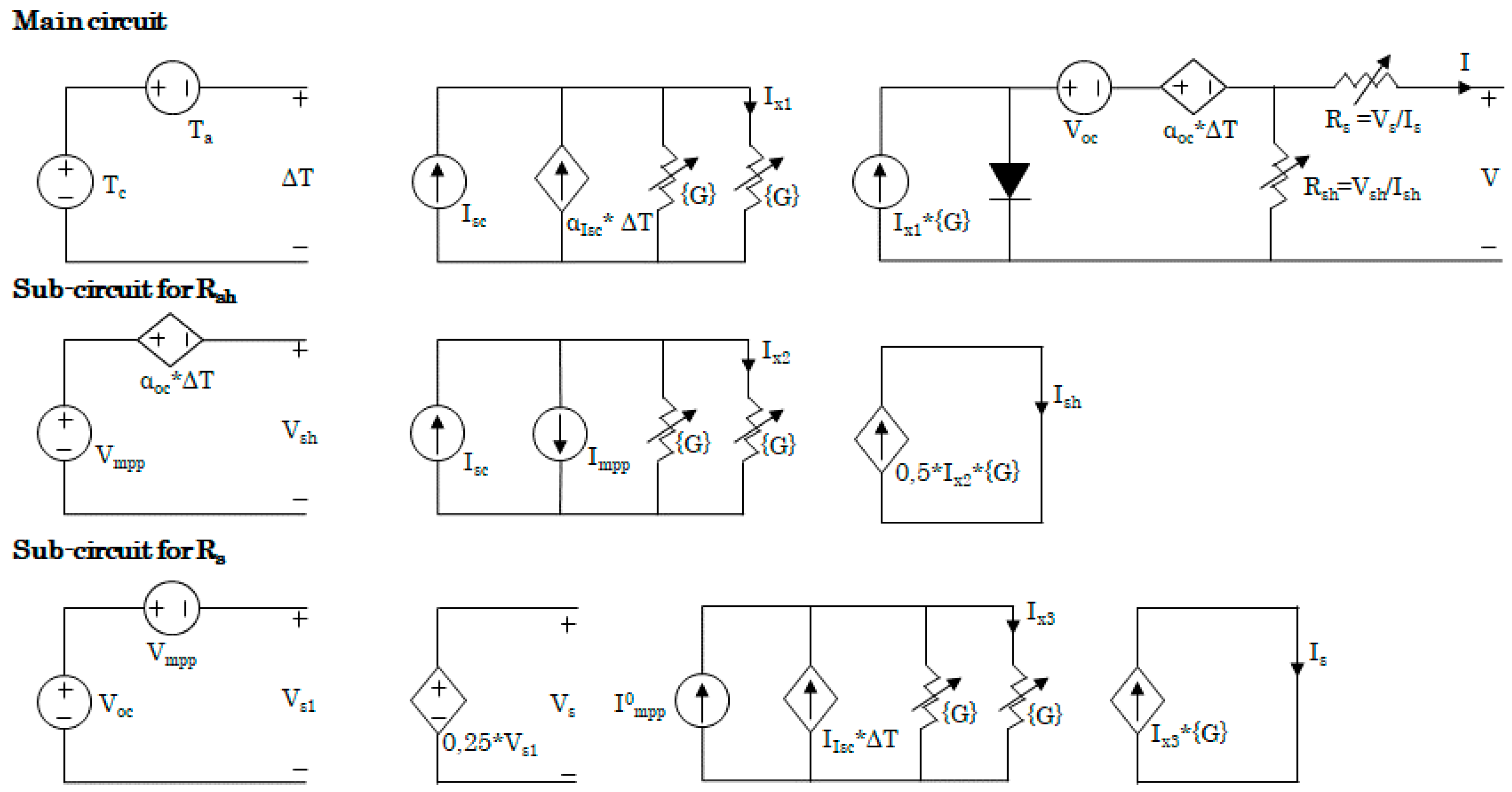
Figure 2 represents the equivalent electric circuit of a single photovoltaic cell. The circuit consists of a main circuit and two sub-circuits to modify R
sh and R
s values when the ambient condition changes, these represent the calculation of the real-time resistors.
The main circuit includes a current source, a diode, two opposite voltage sources and cell dissipate phenomena equivalent resistors which represents the behavior of the cell in open circuit state. The current generated by the light source is modelled through two current sources and a resistor in shunt, which is irradiance dependent. Temperature effects are included as a two-voltage source in series with opposite polarities. The unconnected point at the main circuit represents the output of the cell, the remaining parts are for the configuration of parameters and variables. In order to complete the model, an electric load is connected in parallel with the voltage output of the two branches.
The photovoltaic model is completed with the manufacturer data-sheet and the calculated parameters. The solar harvester devised for this research uses the solar module SLMD481H08 manufactured by IXOLARTM [
23].
The selected monocrystalline module has 88.8 mm of width and 54.7 mm of height. Each individual cell has 20 × 12 mm
2 = 2 × 1.2 cm
2 = 2.4 cm
2. The whole module has 16 cells distributed in two branches connected in parallel, each one made of 8 cells. The cell has a nominal efficiency of 22%. It also has a broad photonic response over a wide range of wavelengths. Thus, it is suitable for both applications, indoor and outdoor. The architecture and dimensions of the module used is shown in
Figure 3.
Electrical characteristics of the selected solar module provided by the manufacturer are presented in
Table 1.
The whole photovoltaic module model is made of single cells (
Figure 2) arranged as a commercial selected photovoltaic module,
Figure 3: 16 main cells in 2 rows/branches of 8 cells each. Simulations provide the maximum out power for the selected ambient conditions [
25].
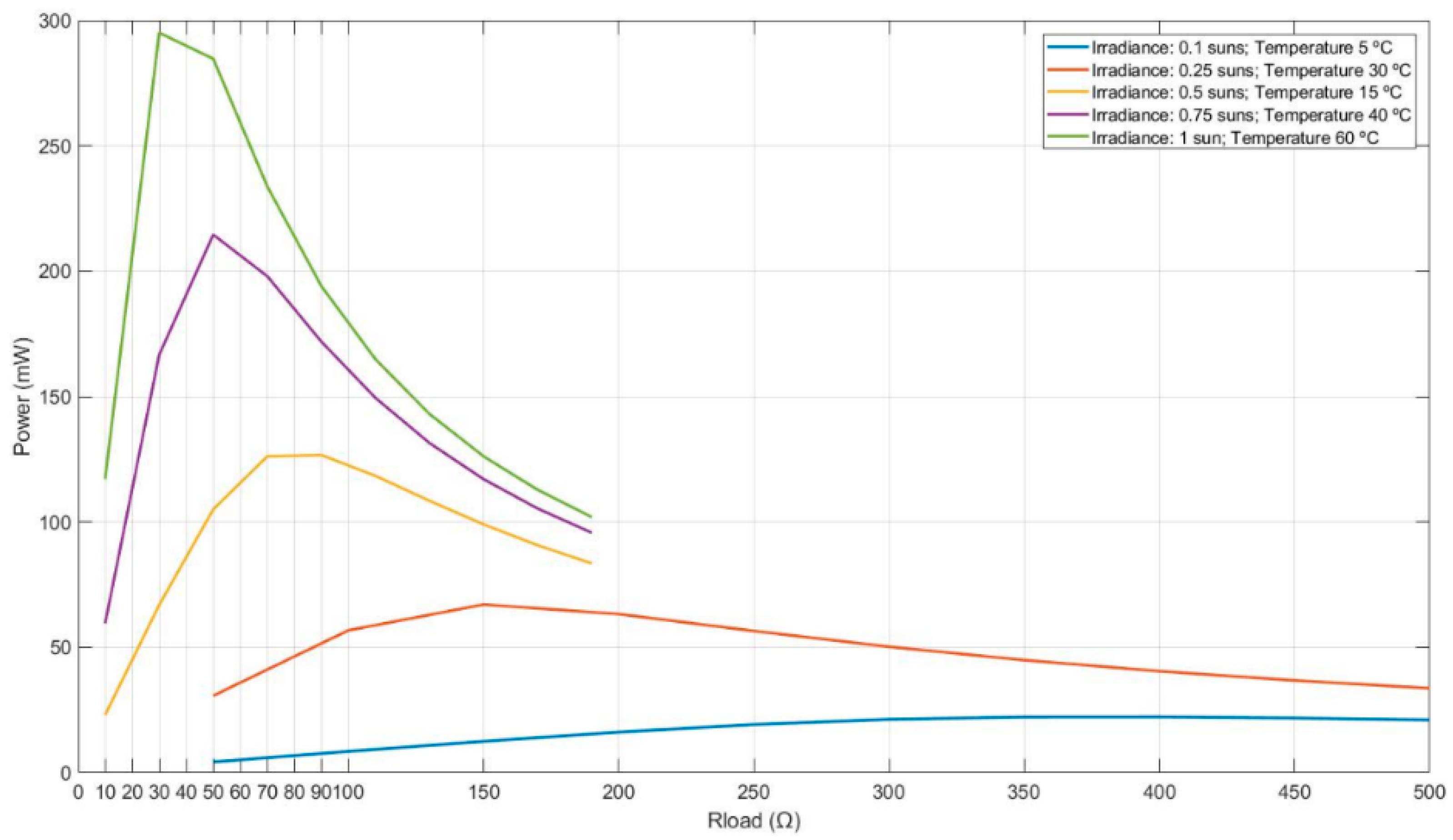
Table 2 and
Figure 4 show the achieved results.
These results show that the cells produce more power at higher temperatures for the same irradiance level. Besides, irradiance has more effect on power production than temperature, e.g., 0.25 sun and 10 °C against 0.1 sun 25 °C. The cell power generation range from 22.333 mW with 0.1 sun at 5 °C to 306.812 mW with 1 sun at 60 °C.
2.2. Model Simulation and Test Results Comparison
In order to verify and validate the accuracy of the photovoltaic electro-physical model, solar tests are carried out. This test is done with a sun luminaire, a controlled source of light. This solar light had the restriction to produce a maximum of 0.5 sun. In addition, a black box is used to avoid any interference of irradiance on the test and maintain the light seal.
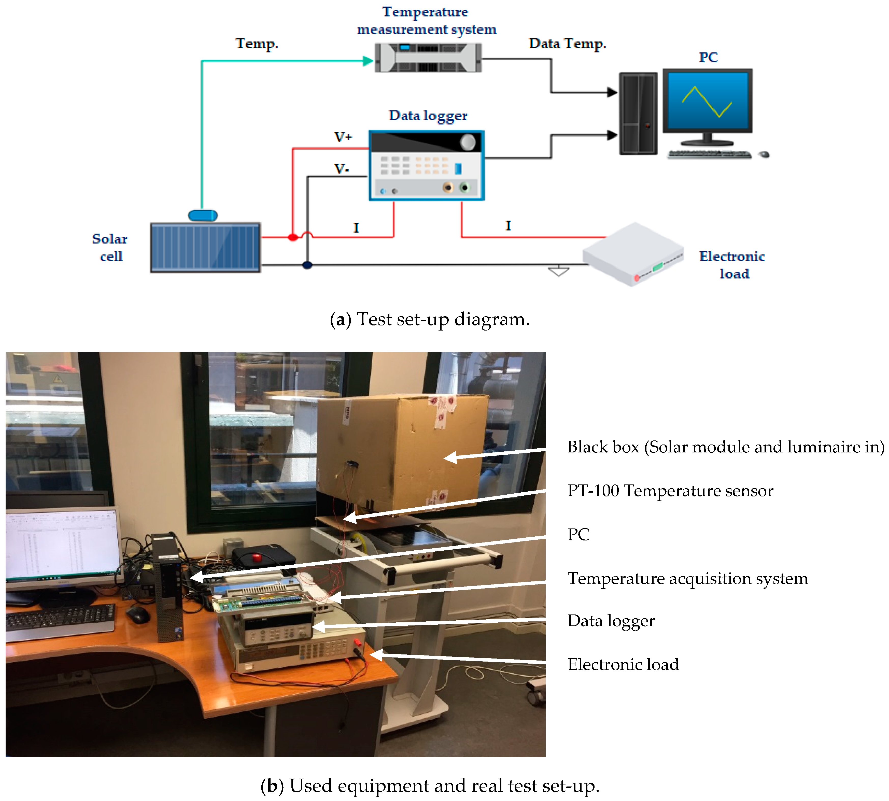
Figure 5a shows the test set-up diagram, and
Figure 5b shows the real implementation of the set-up.
The test procedure has been as follows: The solar module is positioned inside the black box and under the luminaire. The electronic load is connected to the solar cell, for a sweep measurement. A data logger is connected to the solar cell and electronic load in order to measure and register the voltage and current produced by the solar cell. The temperature sensor, PT-100, is located in the box near the solar cell and connected to the temperature measurement system, configured to save data periodically. Finally, the test stars and data is registered for future processing.
Some tests under different irradiance and temperature conditions are developed to verify the model and two of them are shown below under the following conditions:
Then, these tests are compared with electro-physical model simulations. In
Figure 6 and
Figure 7, blue traces represent the simulation results and the orange traces the values measured during the test.
With 0.25 sun and 46 °C, short circuit current is 27 mA,
Figure 6a; MPPT (maximum power point track) is 75 mW and is produced around 3.4 V,
Figure 6b.
With 0.5 sun and 65 °C, short circuit current is 78 mA,
Figure 7a; MPPT is 180 mW and is produced around 2.9 V,
Figure 7b.
In order to verify the model, the deviation between the model values and the data measured is determined, and the results are shown in
Table 3.
In those tests the worst deviation, which is 3.148% in current, occurs when ambient conditions are G = 0.25 sun and T = 46 °C, with 3.148% in current and 3.009% in potency. The lower deviation is produced in G = 0.5 sun and T = 65 °C test, with 2.316% in current and 2.395 in potency. The obtained results confirm that the model is appropriate and can be used in the research.
3. Direct Current (DC)/DC Converter
Usually, the DC/DC converter is placed between the harvester and the storage device as the power manager. The system block diagram with the harvester (photovoltaic cell), power management (DC/DC converter) and the storage device (supercapacitor) is shown in
Figure 8.
The main objective of this subsection is to research, simulate and verify the DC/DC converter for the photovoltaic cell, considering all operating voltage and frequency ranges, and assuming an efficiency greater than 80%.
The DC/DC converter requirements are:
Impedance matching between source and load for maximum energy transference.
To step up the voltage received from harvesting.
To maintain operation functionality and efficiency with sun irradiance as well as with artificial light irradiance.
MPPT control algorithm.
3.1. Boost Architecture and Control Definition
3.1.1. Boost Architecture
The architecture employed in the DC/DC converter is the boost topology [
26,
27] showed in
Figure 9. The main challenge of the design of this converter is that it must manage low power levels and voltage [
28], which limits the performance and availability of the semiconductors.
Boost control techniques are based on the change of the duty cycle value. This element controls the steady-state output concerning the input voltage [
29]. The DC/DC converter construction starts with the selection of the coil value, MOSFET, and diode appropriate devices. This selection has been made bearing in mind two extreme temperature and illumination operation conditions:
The selection of the coil value and MOSFET and diode devices was performed with Linear Technology Simulation Program with Integrated Circuits Emphasis (LTSPICE
®) [
30], however other simulation packages could be used.
3.1.2. Control Definition
Nowadays, most converters have two modes of operation or control schemes, a continuous mode with pulse frequency modulation (PFM) or pulse wide modulation (PWM) control for maximum output power; i.e., maximum load and discontinuous control mode (DCM) with variable frequency for low loads or unloaded condition, which can be implemented through current or voltage control loops. The DCM improves the quiescent current of the converter, and, consequently, its efficiency [
29]. Besides, most DC-DC converters for photovoltaic (PV) modules employ different types of MPPT control algorithms in order to drain, at any time, the maximum power that the PV module provides. The basic form of MPPT tracking algorithm employs the measure of input power and adjust the DC-DC control signal accordingly to get the maximum power the PV could deliver regardless the load demands, the eventual excess or lack of energy should be absorbed of provide by a backup storage device: battery or supercapacitor. In the literature could be found many types of MPPT algorithms [
31]. Thus, the control of the DC-DC converter must include an MPPT control algorithm.
The switching frequency of the converter constitutes a key parameter to improve maximum efficiency, and it is related with the power input condition. Therefore, the goal is to minimize the switching losses in the converter, it is done reducing the frequency and choosing active devices that provide less switching losses. On the other hand, there is the issue of component size, the higher the frequency, the smaller the inductance and capacitor values and sizes will be, and consequently, the lower the losses in the inductance serial resistance and the voltage drop in Equivalent Series Resistance (ESR) of the capacitors. The aforementioned is achieved at the expense of increasing the switching losses.
In the present study, the DC-DC converter is of low power, therefore the control frequencies may range from 10 kHz to tenths of MHz, more concretely to hundreds of kHz are shown in
Section 3.4.
3.2. MOSFET Selection
At minimum temperature conditions and irradiance, the switching frequency is set to 50 kHz, the duty-cycle to 0.15, the coil inductance to 270 µH, the R
load to 400 Ω and the selected commercial diode model is the MBR0520L. Next, several commercial MOSFETs are selected to test on the basis of their appropriate characteristics for the present case in use:
Table 4. At maximum ambient conditions, the switching frequency is set to 20 kHz, the duty-cycle to 0.16, the R
load to 50 Ω and the coil value and diode are maintained.
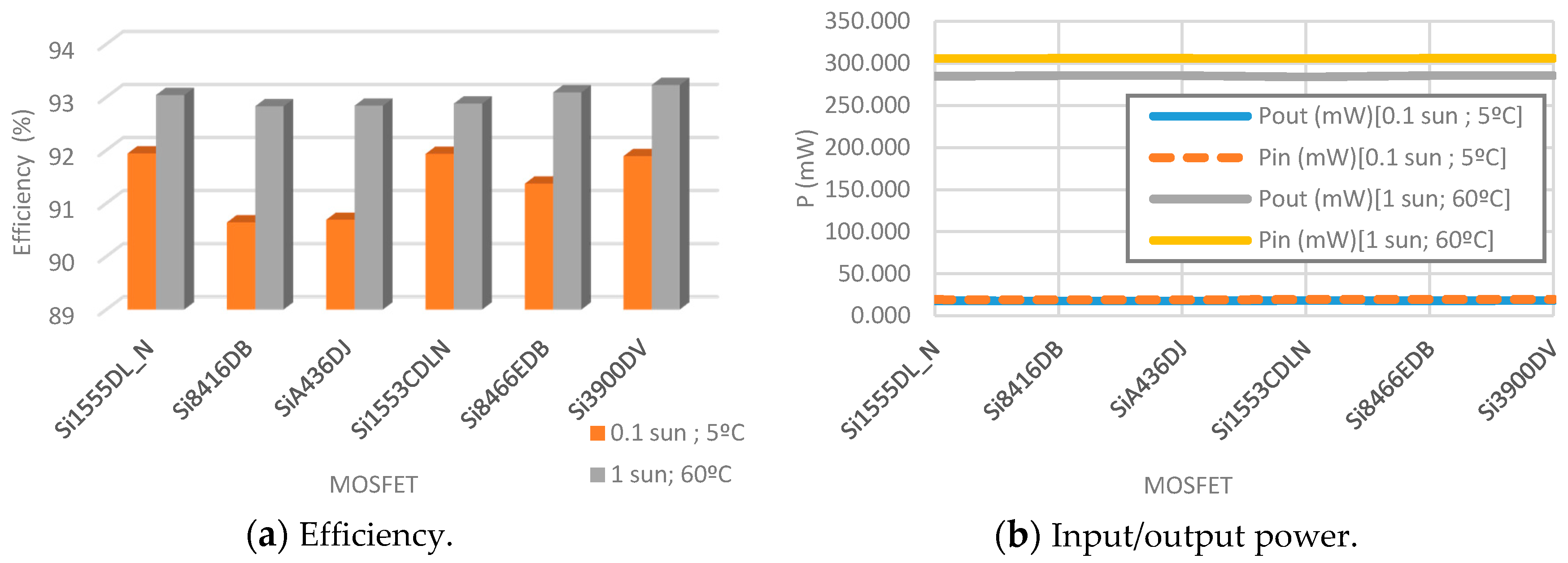
Table 4,
Table 5 and
Figure 10 summarize the results with detailed conditions.
The results obtained show that the efficiency for both conditions is higher than 90% with all MOSFETs. Moreover, with low light irradiance and temperature they reach up to 91% and in high conditions up to 93%. Si1555DL_N and Si3900DV present the best efficiency regarding the rest of the devices. However, Si1555DL_N and Si1553CDLN have the least consumption at both work operation modes. Because of these reasons, Si1555DL_N MOSFET is selected to be the MOSFET at the DC/DC boost converter. However, Si3900DV is also a feasible alternative to be used.
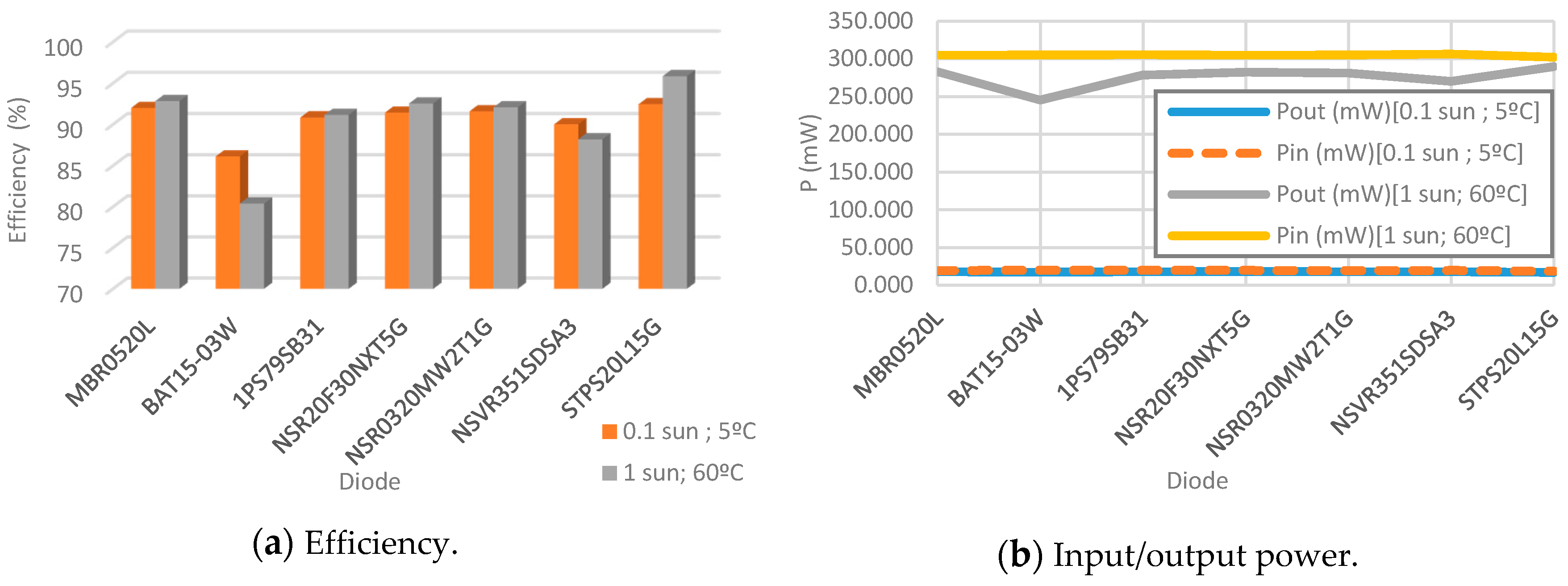
3.3. Diode Selection
The diode is selected employing the same procedure as with the MOSFET, the same minimum circuit values are adopted. So, several commercial diodes are selected on the basis of their characteristics for the present case in use:
Table 6. In
Table 6,
Table 7 and
Figure 11 the results achieved with the conditions detailed are shown.
Efficiencies in this case at both conditions are higher than 90% with the exception of the BAT15-03W diode. Moreover, in low light and temperature ambient they reach up to 92% and in high conditions up to 95%. STPS20L15G and MBR0520L present the best efficiency regarding the rest of the diodes. However, with STPS20L15G converter, efficiency is 0.4% higher at the worst ambient conditions and 3% better in the best ambient conditions. Due to these reasons, the STPS20L15G diode is selected for the DC/DC boost converter. However, after having issues with the PSPICE model of the STPS20L15G diode, MBR0520L is used for simulations because it has a proper response too. Nevertheless, it is recommended to keep track continuously of the new releases of the diode manufacturer in order to consider STPS20L15G.
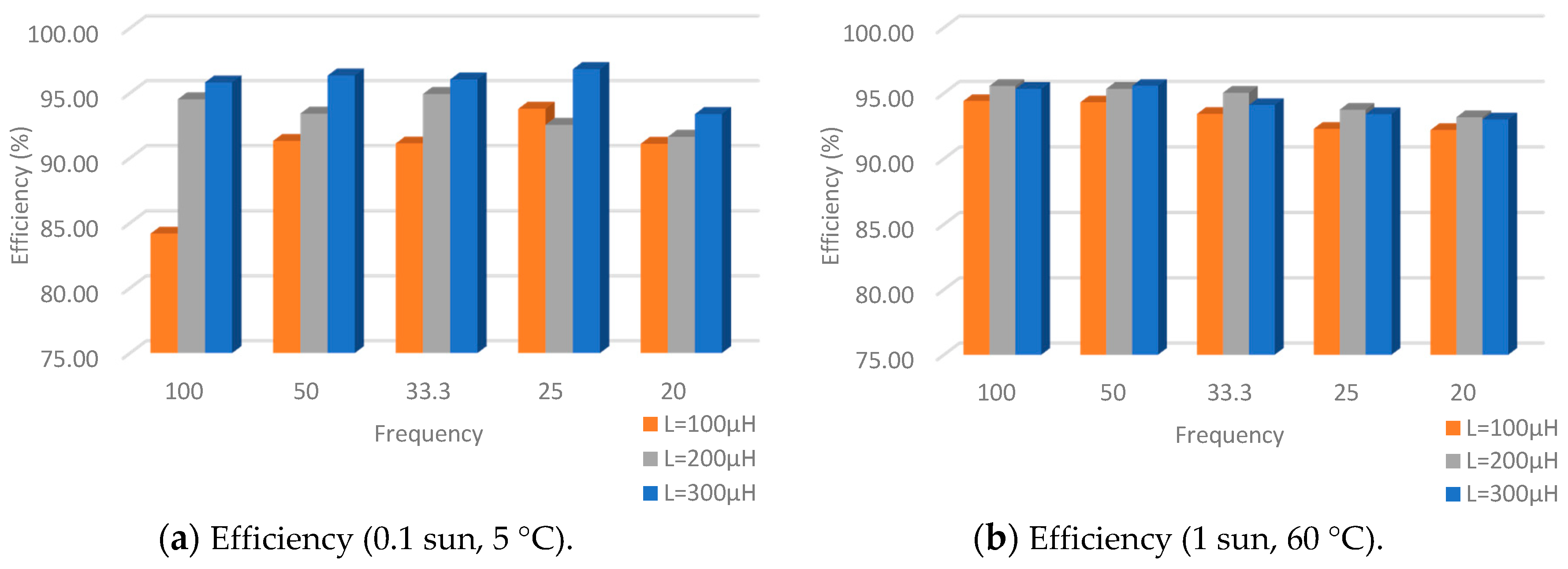
3.4. Coil and Switching Frequency Selection
With minimum ambient conditions, the duty-cycle is set to 0.2, the R
load to 2 kΩ and the selected diode in the previous section. In the
Table 8,
Table 9 and
Figure 12 the results achieved with the conditions detailed are shown.
If input/output power is taken into account, the simulation results show that the most suitable value for the coil is 200 µH. With 0.1 sun and 5 °C temperature condition the best coil value is 100 µH and with 1 sun and 60 °C temperature the best coil is 300 µH. However, the coil values for maximum and minimum extreme conditions are not adequate for nominal conditions; consequently, 200 µH is an intermediate value which gives stability.
The performed test shows that 100 kHz provides the best performance at low input power levels, and 20 kHz provides the best performance for high input power levels. Thus, in order to obtain get the maximum efficiency from the converter, its switching frequency should be dynamically changed between the previous values depending on the ambient conditions and the power input ranges or a trade of the previous frequencies [
45].
3.5. Simulations and Results of the Converter. Duty-Cycle and Resistive Load
After making the selection of the components and establishing operation modes of control, several simulations have been carried out to analyze, adjust and obtain the maximum efficiency of the converter at different ambient conditions and input power levels.
The MPTT control algorithm of the DC-DC converter guaranties that the input power is delivered to the load with maximum efficiency, but the maximum power transfer occurs when the source and the load are matched, which is not always feasible. In solar farms this issue does not exists for the electrical grid absorbs the fluctuations. Therefore, in order to further improve the energy efficiency, it should be required a technique to dynamically change the load. This could be achieved by means of an energy storage device, battery or supercapacitor, and controlling the energy it stores or deliver. In doing so, it is required to know the load consumption patterns and the optimum loads of the PV and DC-DC converter, [
46] analyses DC-DC power supply systems for pulsed loads from maximum efficiency perspective.
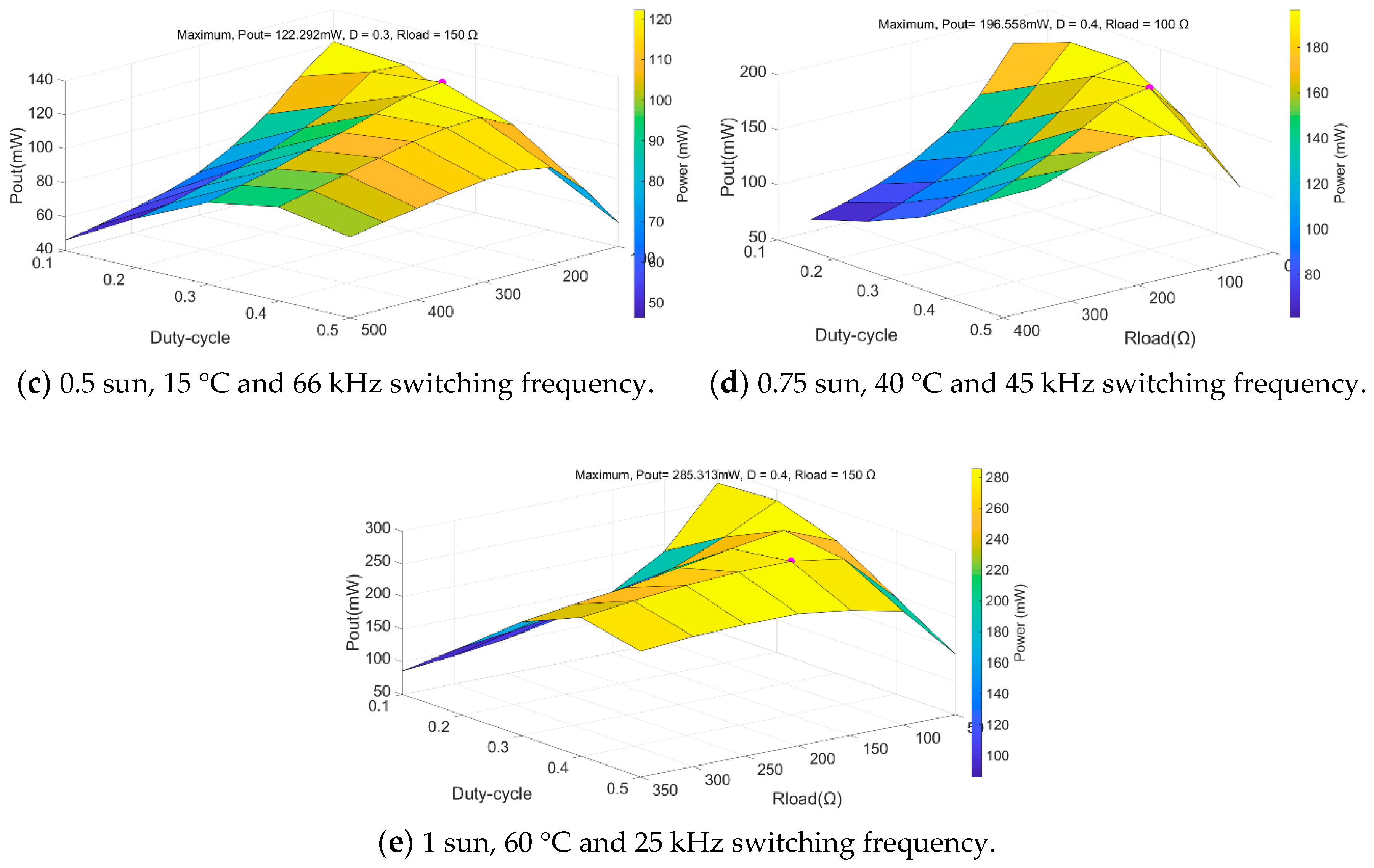
In order to identify the optimum values of load and duty-cycle, and dimension, accordingly, the energy storage device, a load and duty-cycle sweep is performed in five ambient condition ranges.
Figure 13 shows the sweep results obtained.
In the first case (
Figure 13a), the highest output power is 21.247 mW and is obtained with 0.2 duty-cycle and 500 Ω resistive load. In the second case (
Figure 13b), the highest output power is 61.476 mW and is obtained with 0.3 duty-cycle and 400 Ω resistive load. In the third case (
Figure 13c), the highest output power is 122.292 mW and is obtained with 0.3 duty-cycle and 150 Ω resistive load. In the fourth case (
Figure 13d), the highest output power is 195.57 mW and is obtained with 0.3 duty-cycle and 100 Ω resistive load. In the fifth case (
Figure 13e), the highest output power is 283.18 mW and is obtained with 0.2 duty-cycle and 50 Ω resistive load.
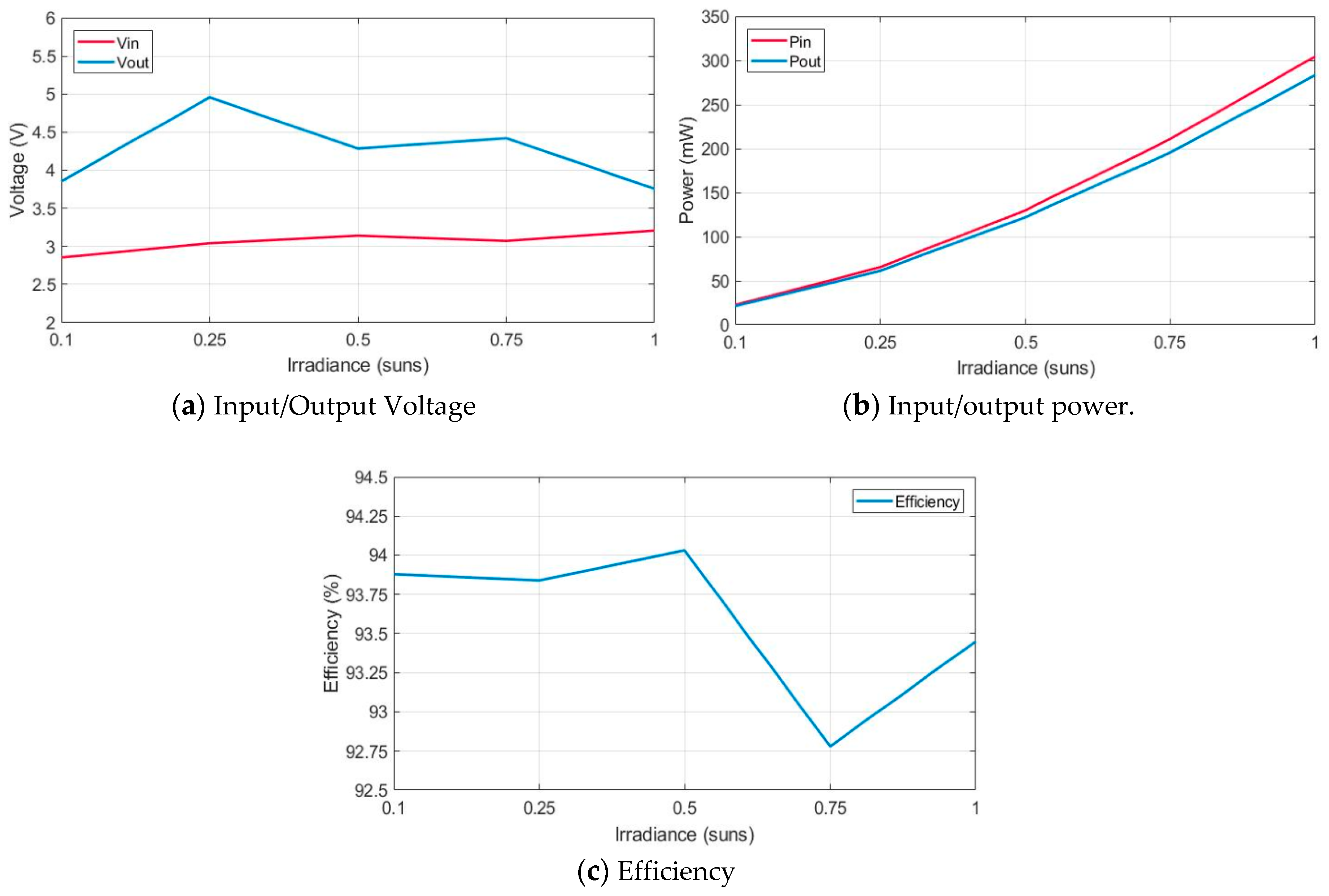
Table 10 and
Figure 14 summarize maximum output values obtained in previous simulations for different irradiance and temperature levels: from 0.1 sun and 5 °C to 1 sun and 60 °C.
Table 10 and
Figure 14a show the evolution of the input (V
in) and output (V
out) voltage levels at the different environment conditions considered. The DC/DC converter provides an output voltage between 3.7 V and 4.9 V, this range is into the most common range of power supply voltage in consumer electronics. The results in
Figure 14b show that the power increases linearly with irradiance. Moreover, whenever the input irradiance power increases, so does the difference between input and output power because the system efficiency diminishes. Besides,
Figure 14c shows that the efficiency is always much greater than the 80% considered in
Section 2 for the DC/DC converter architecture, which correspond to the expected efficiency of commercial boost converters [
47,
48]. The highest efficiency is 94.03%, and occurs at 0.5 sun and 15 °C; and the lowest efficiency (92.30%), is obtained at 0.75 sun and 40 °C.
4. Conclusions
Energy harvesters are being increasingly used for gathering energy from the environment and feeding electronic circuits without the help of a mains power grid connection or battery back-up support. An energy harvester system needs management control, and in this work a DC/DC converter is proposed for a photovoltaic harvester after the analysis of different possible devices, looking at different parameters such as efficiency, power and voltage.
A boost architecture is chosen for the DC/DC converter, and between considered devices the chosen ones are: the MOSFET Si1555DL_N (Si3900DV is adequate too), the diode STPS20L15G (MBR0520L is adequate too), the suitable value for the coil is 200 µH, the switching frequency must be dynamic between 150 kHz and 20 kHz depending on the input condition. Finally, the appropriate duty-cycle and resistive load for each input case are analyzed, the best results are obtained with a duty-cycle between 0.2 and 0.3, and the load between 50 Ω and 500 Ω.
The results show that proposed harvesting system works properly for the considered ambient conditions.

