Decawave UWB Clock Drift Correction and Power Self-Calibration

 ,
, 
Abstract
:1. Introduction
2. Decawave UWB
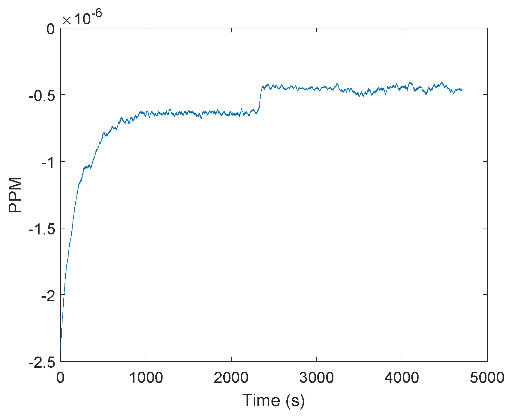
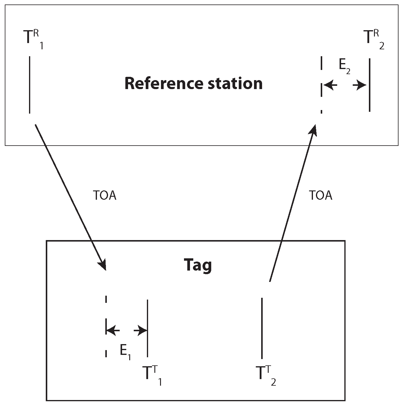
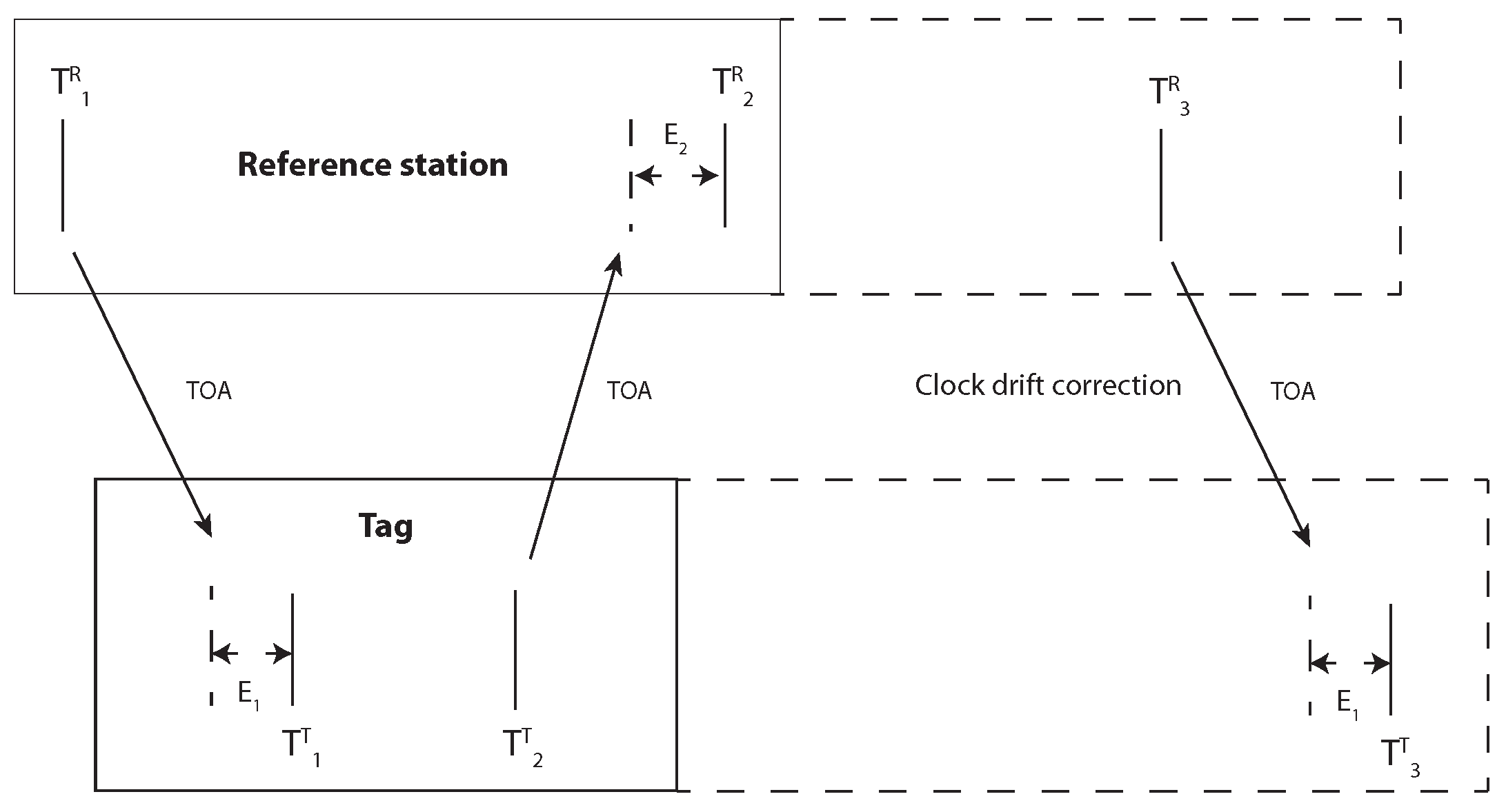
3. Clock Drift Correction
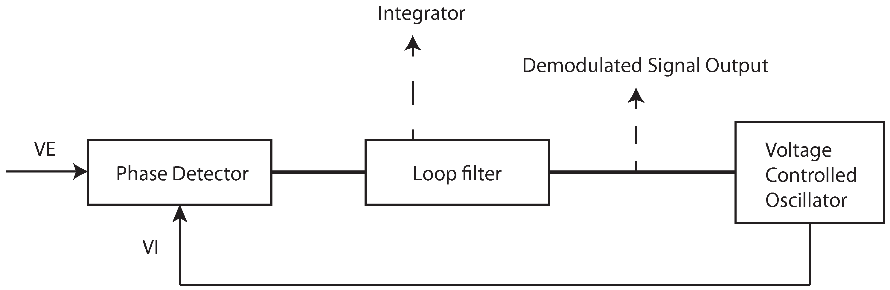
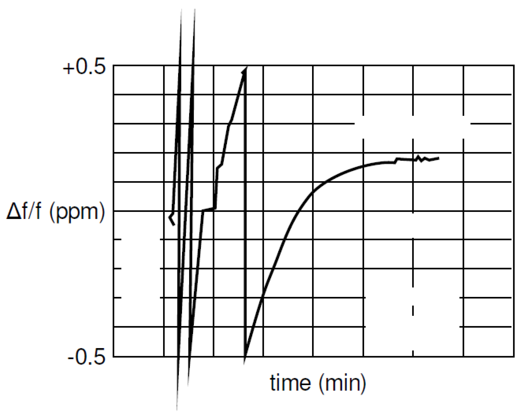
3.1. General Approach
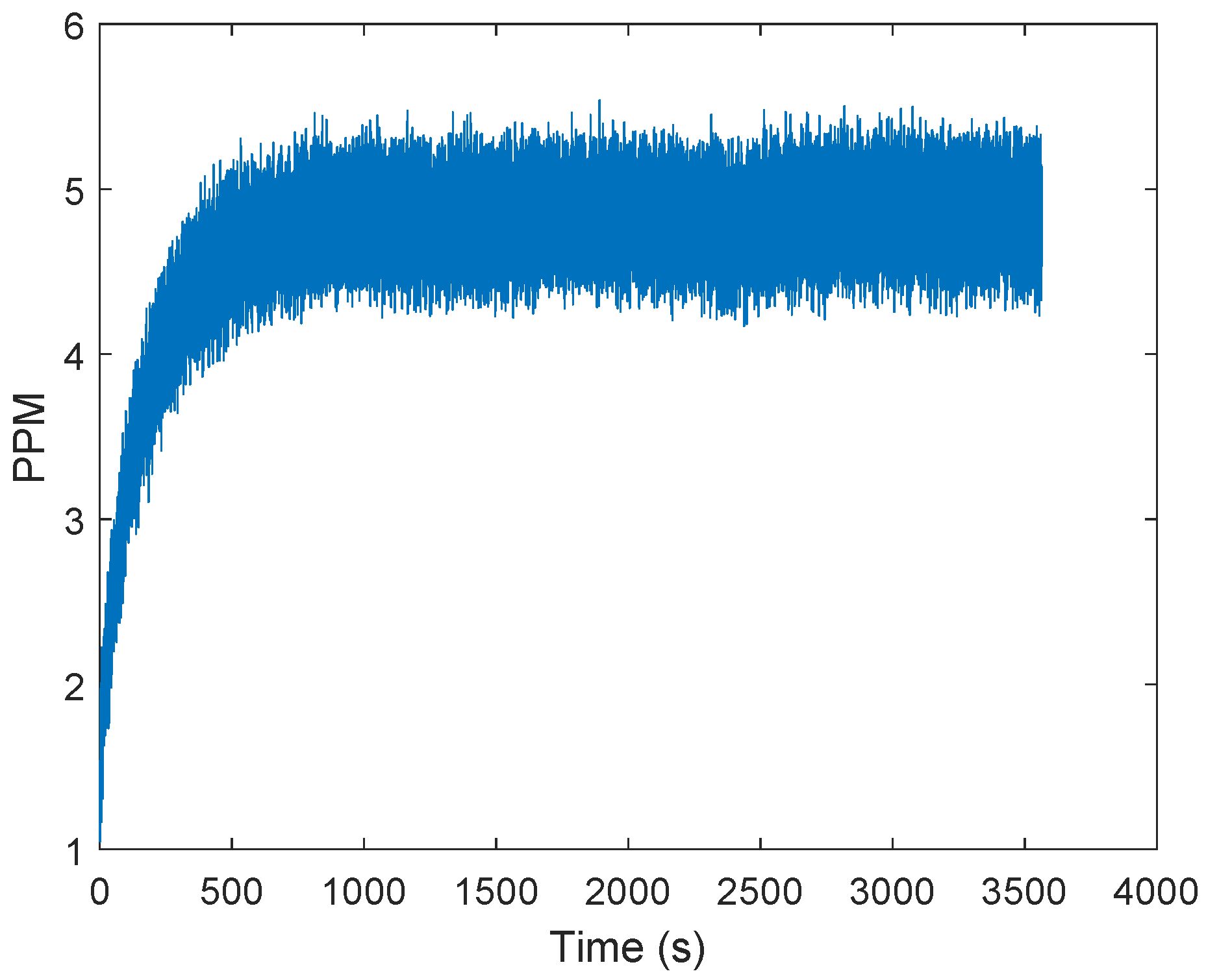
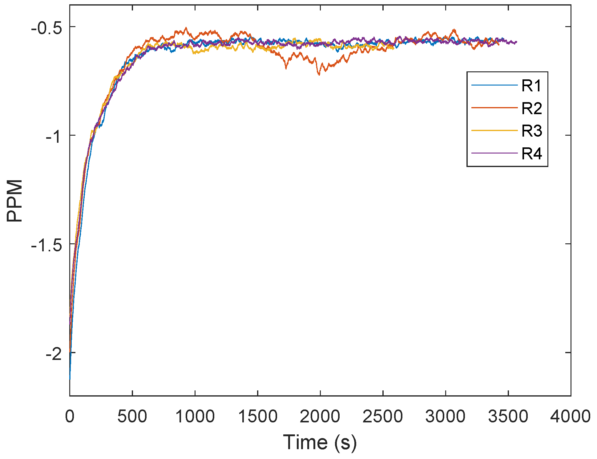
3.2. Proposed Approach for the Clock Drift Correction
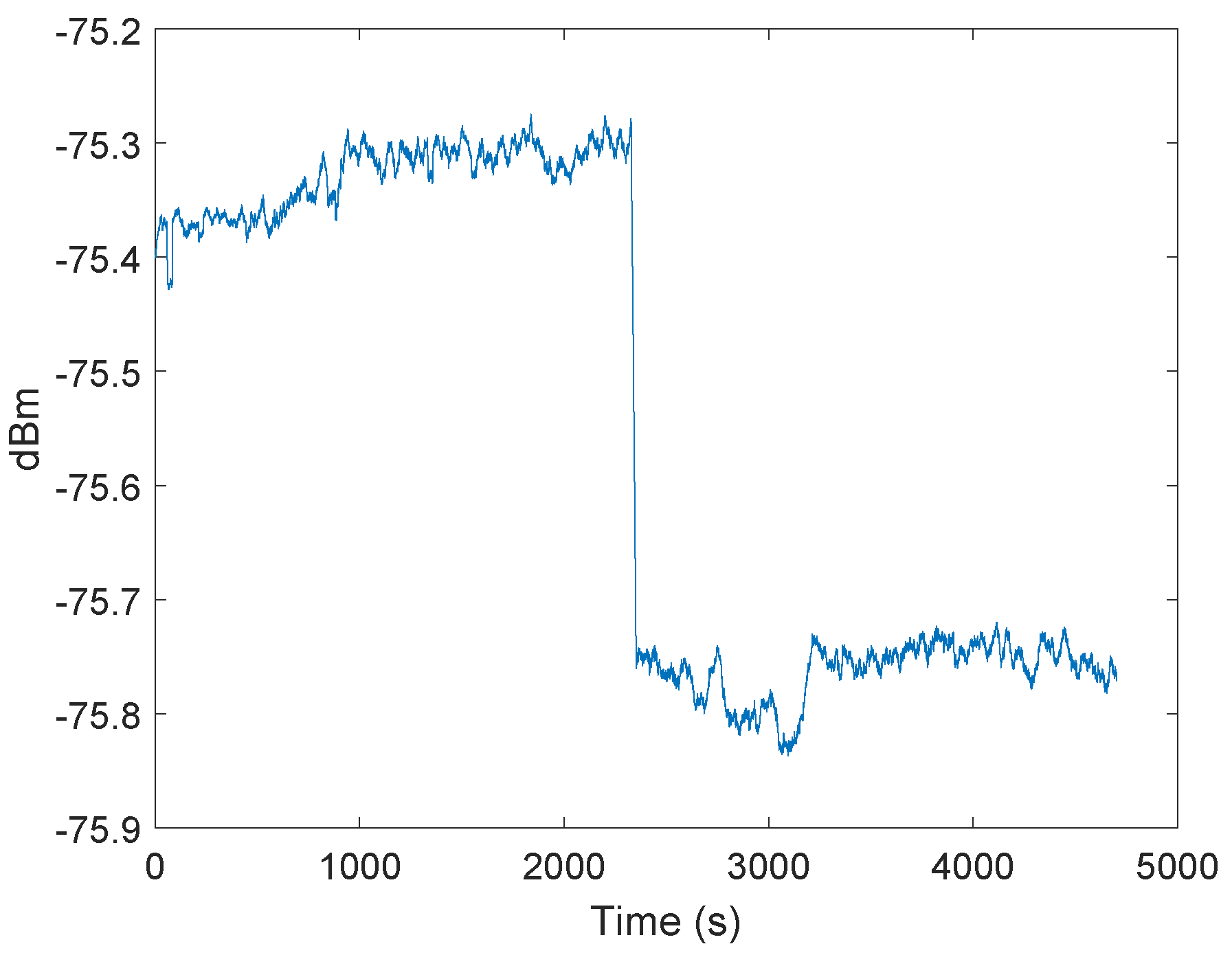
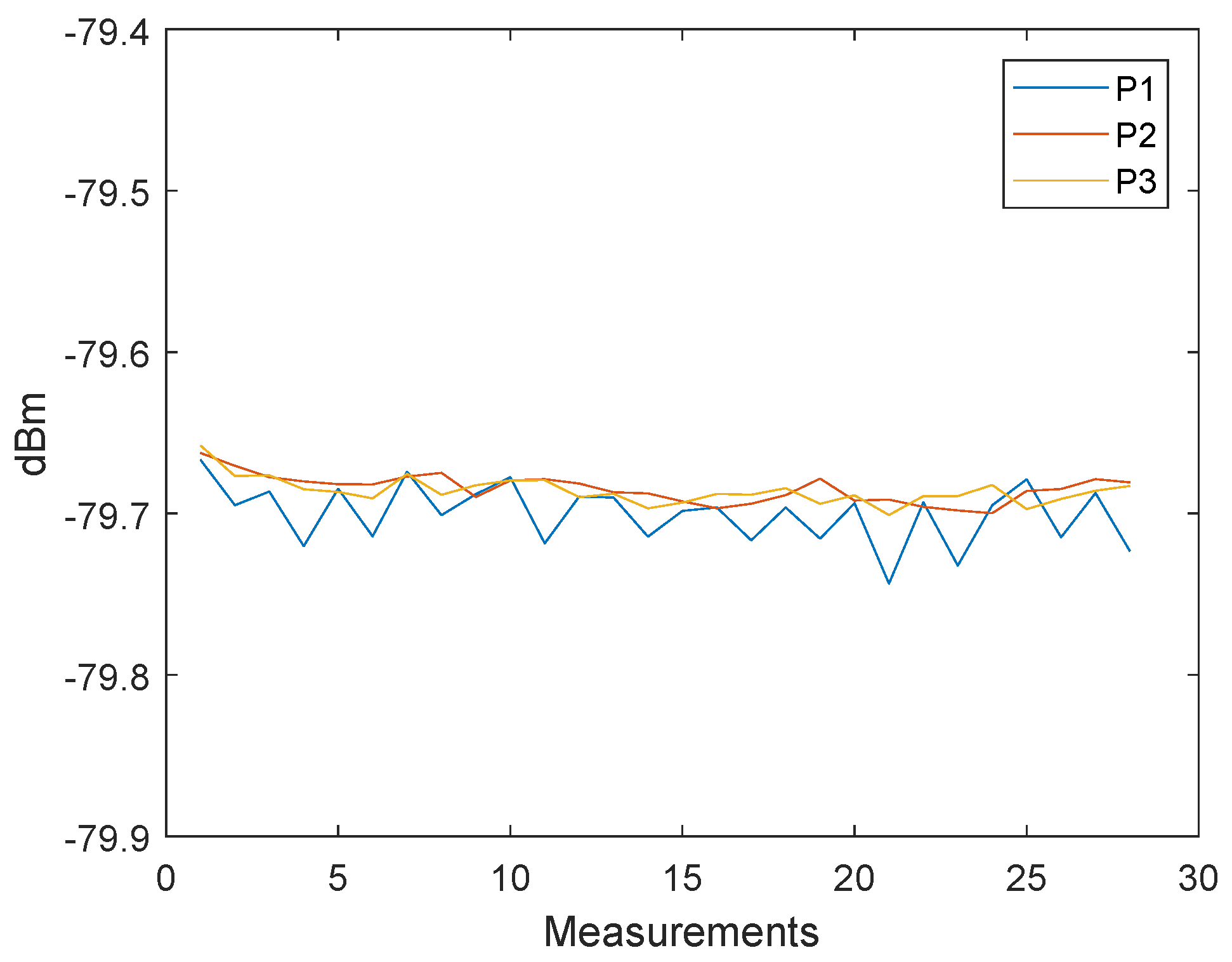
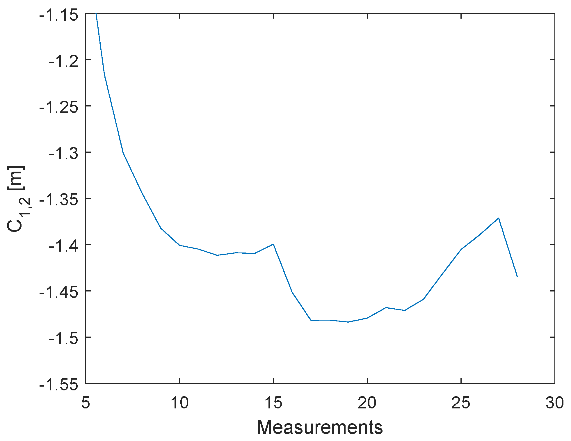
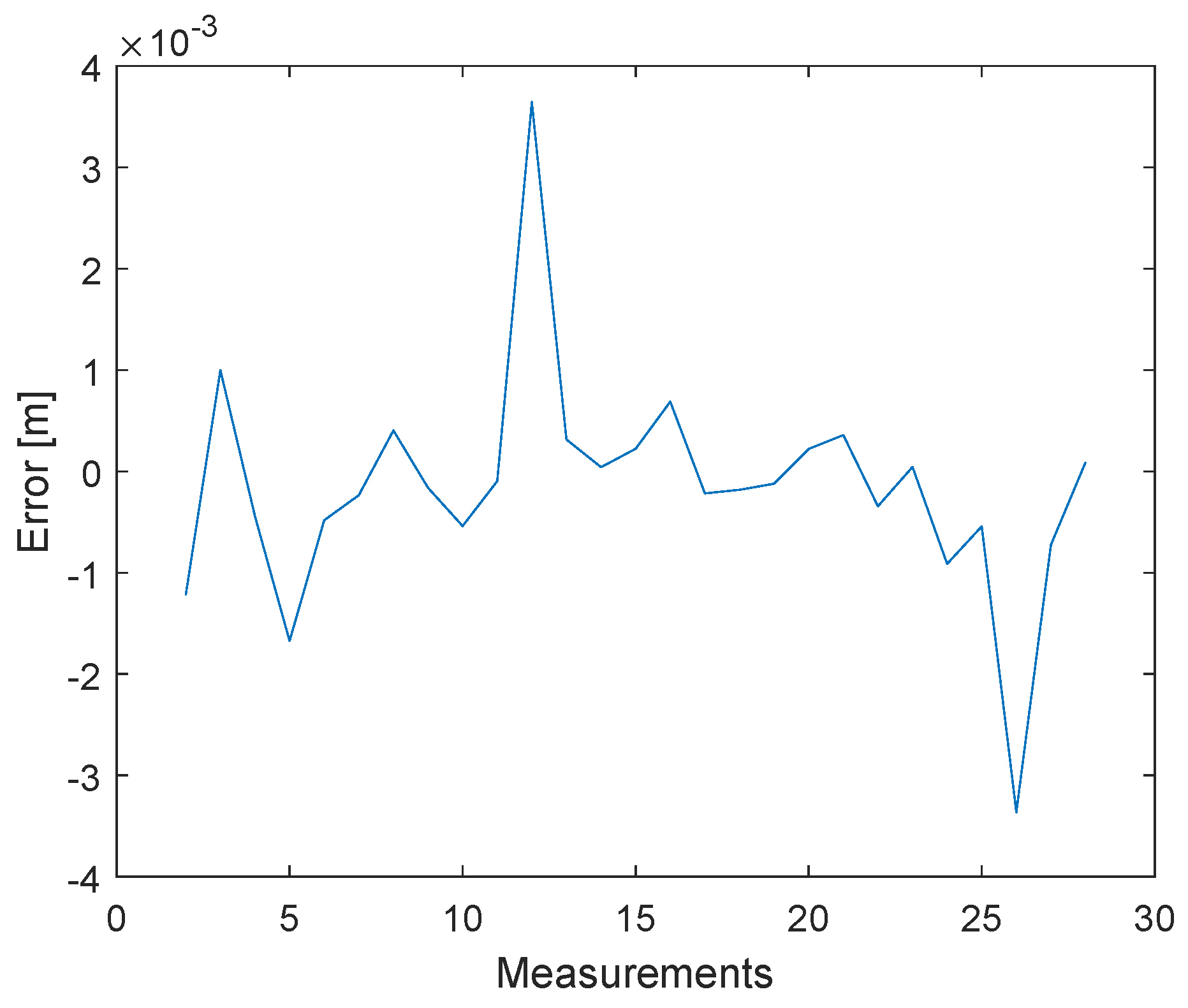
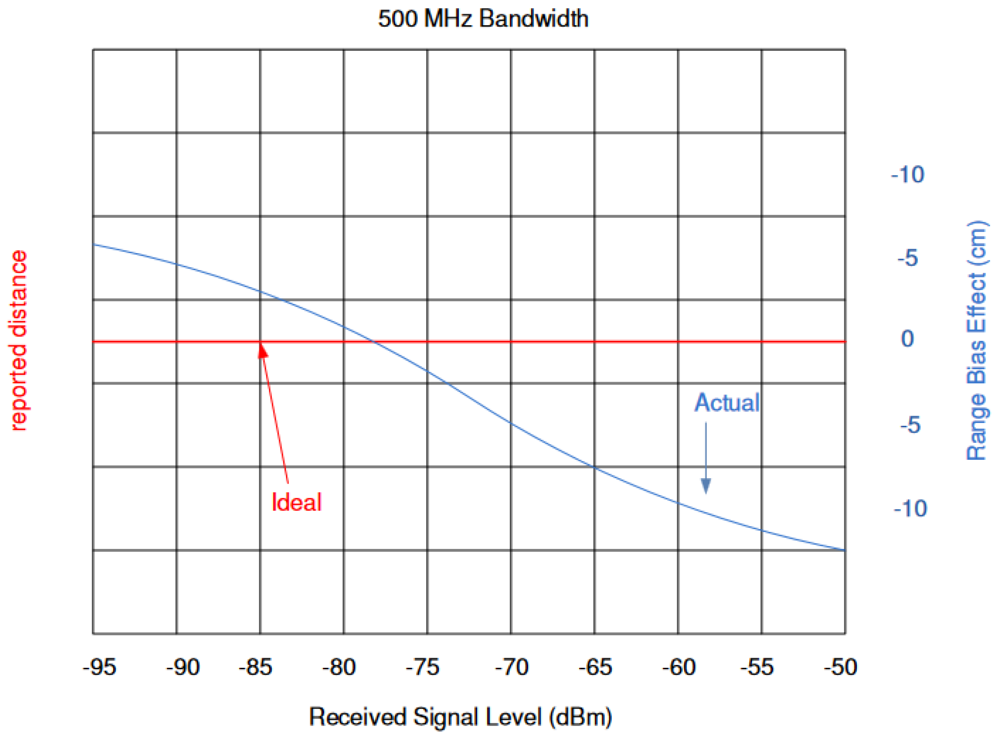
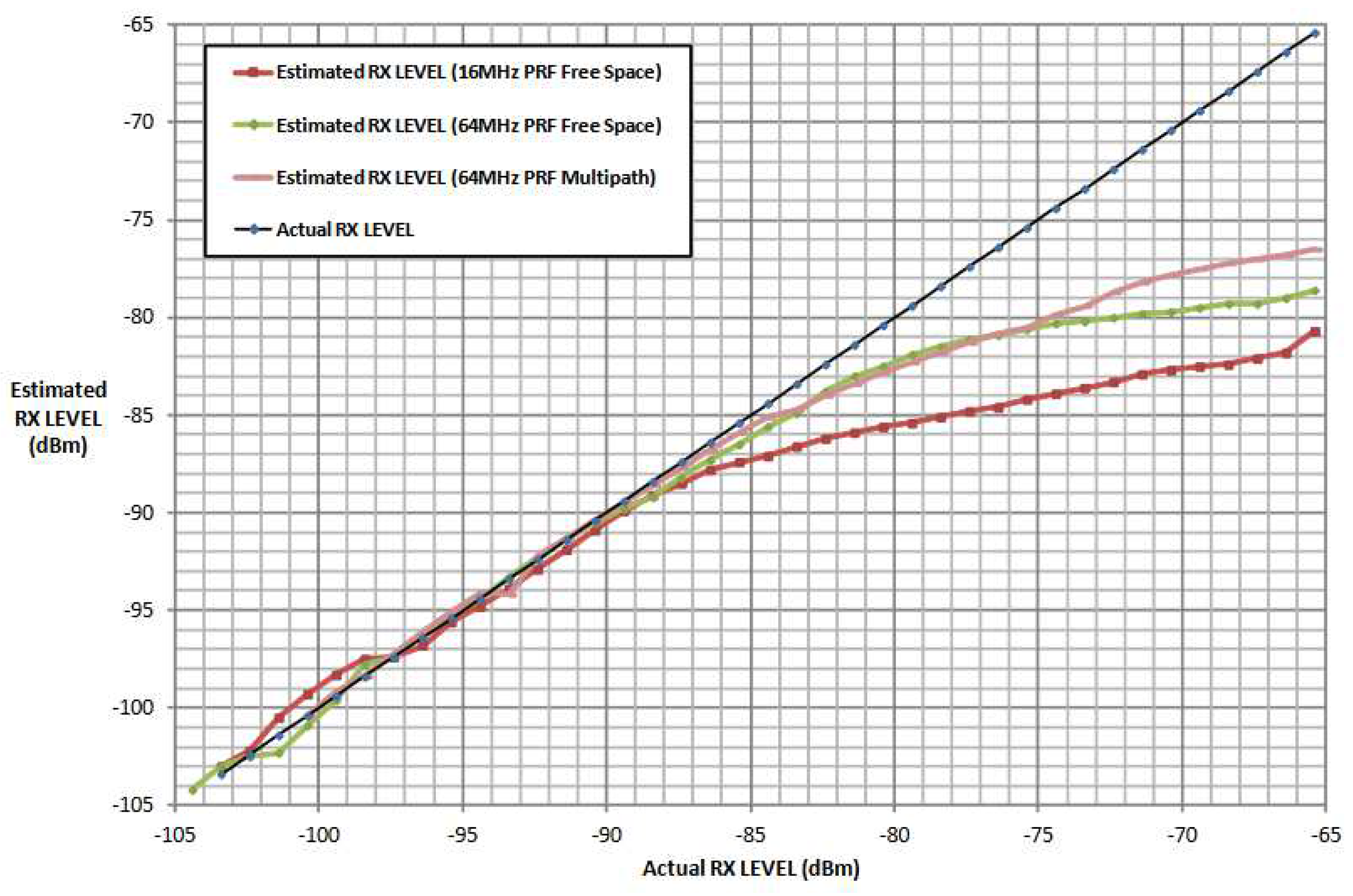
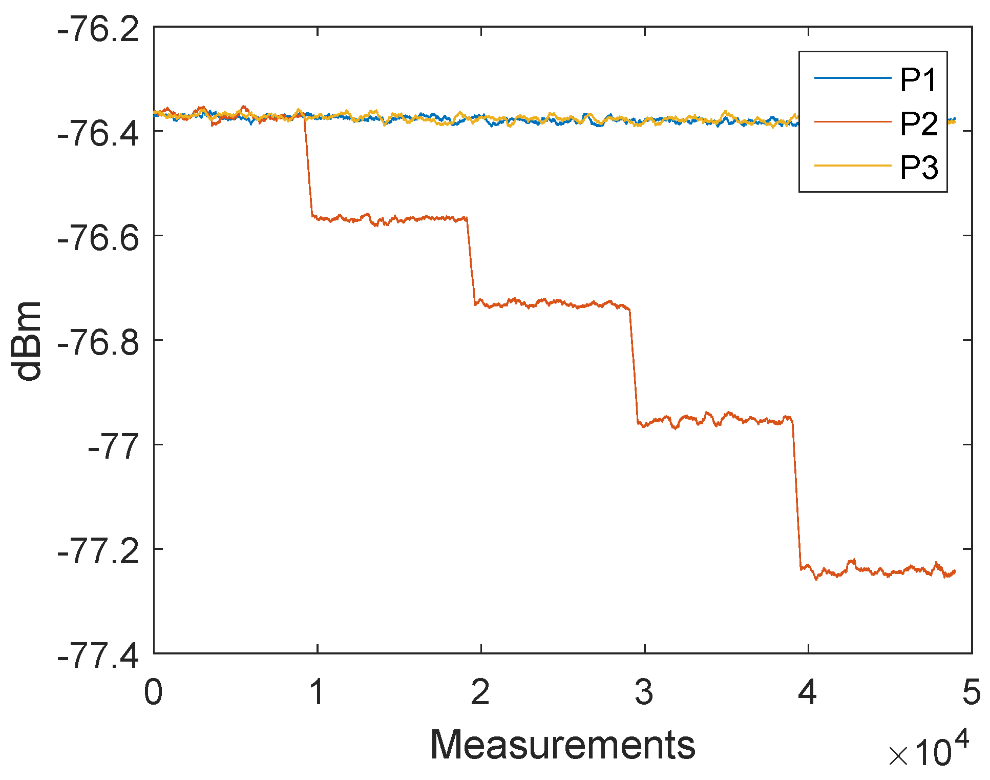
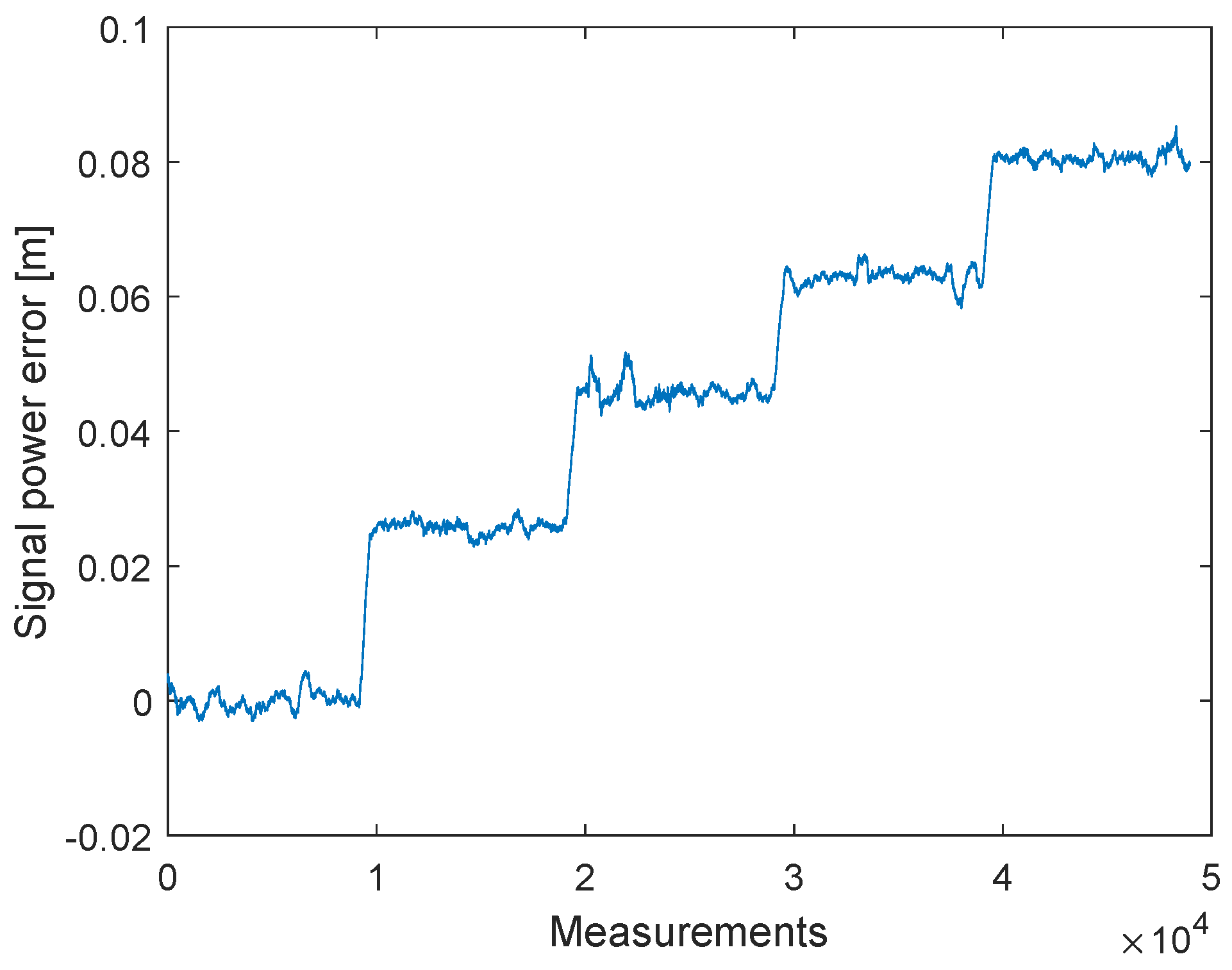
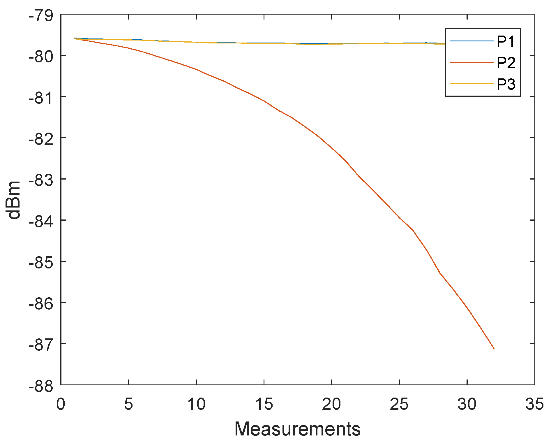
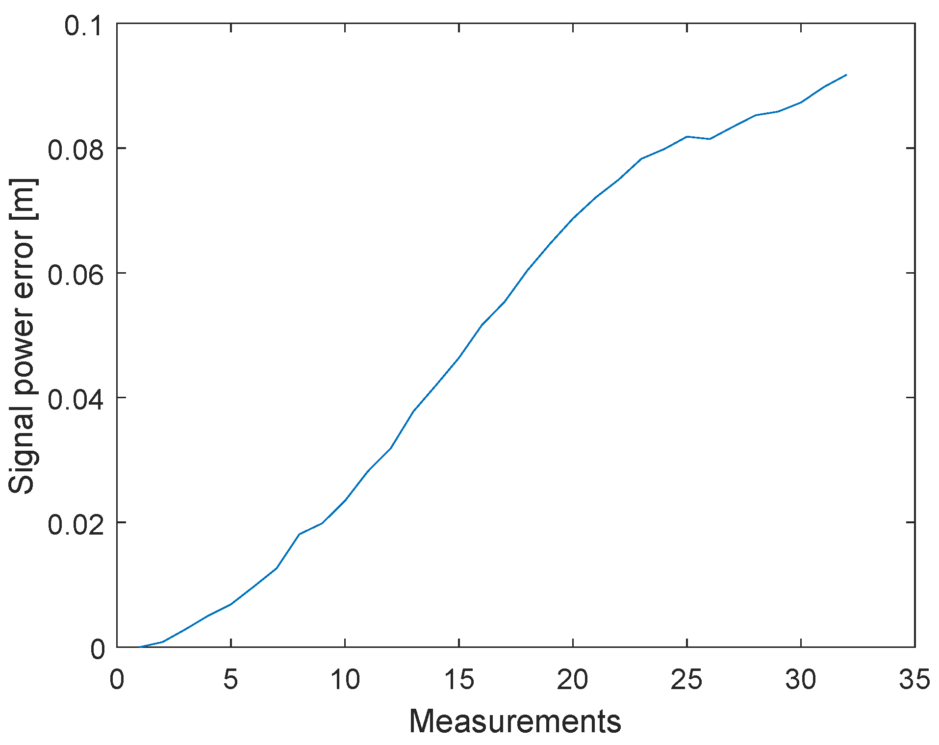
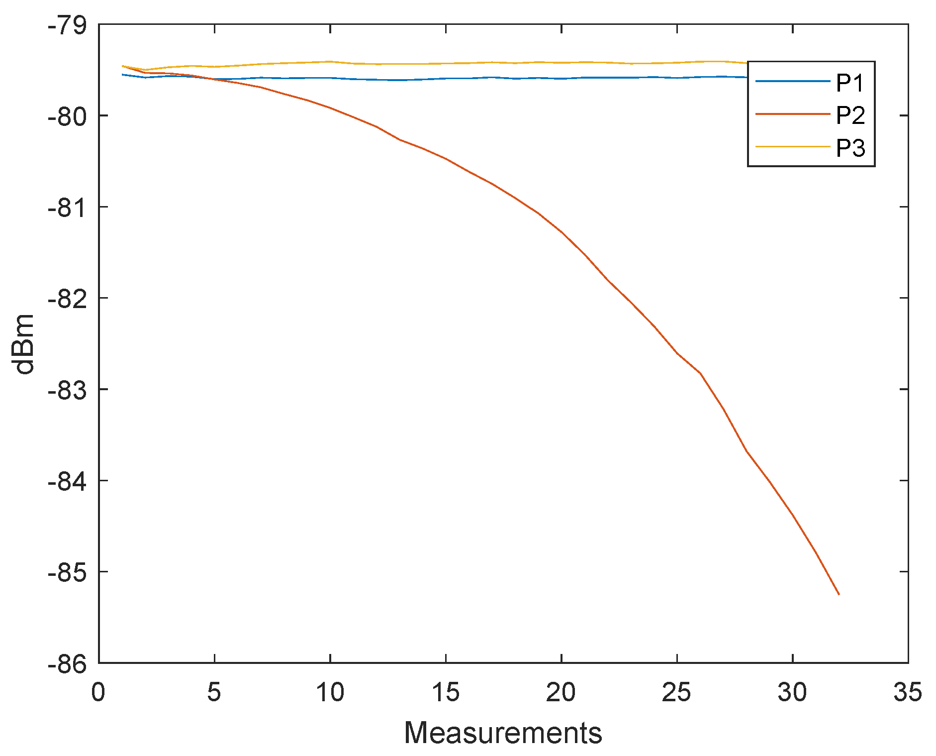
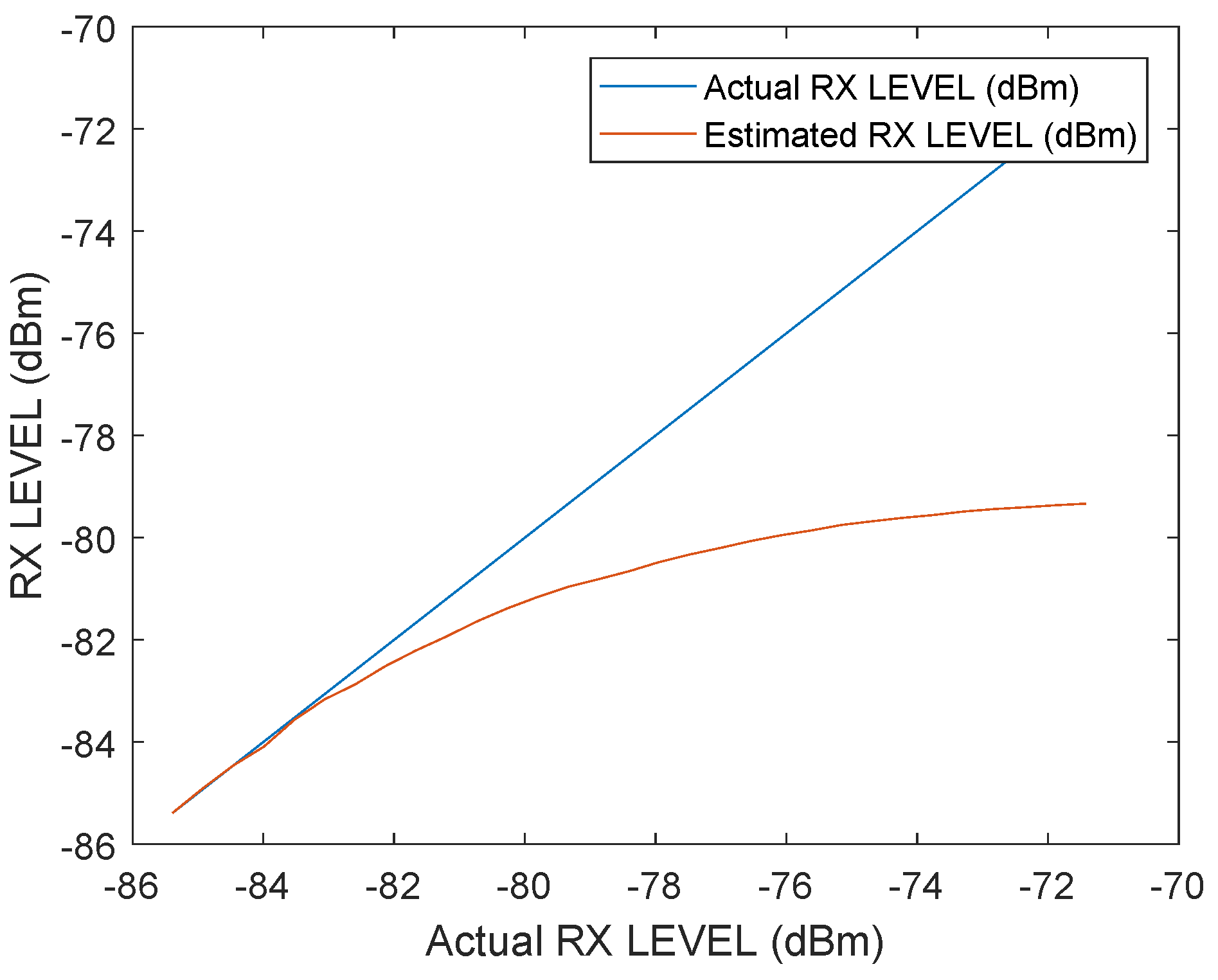
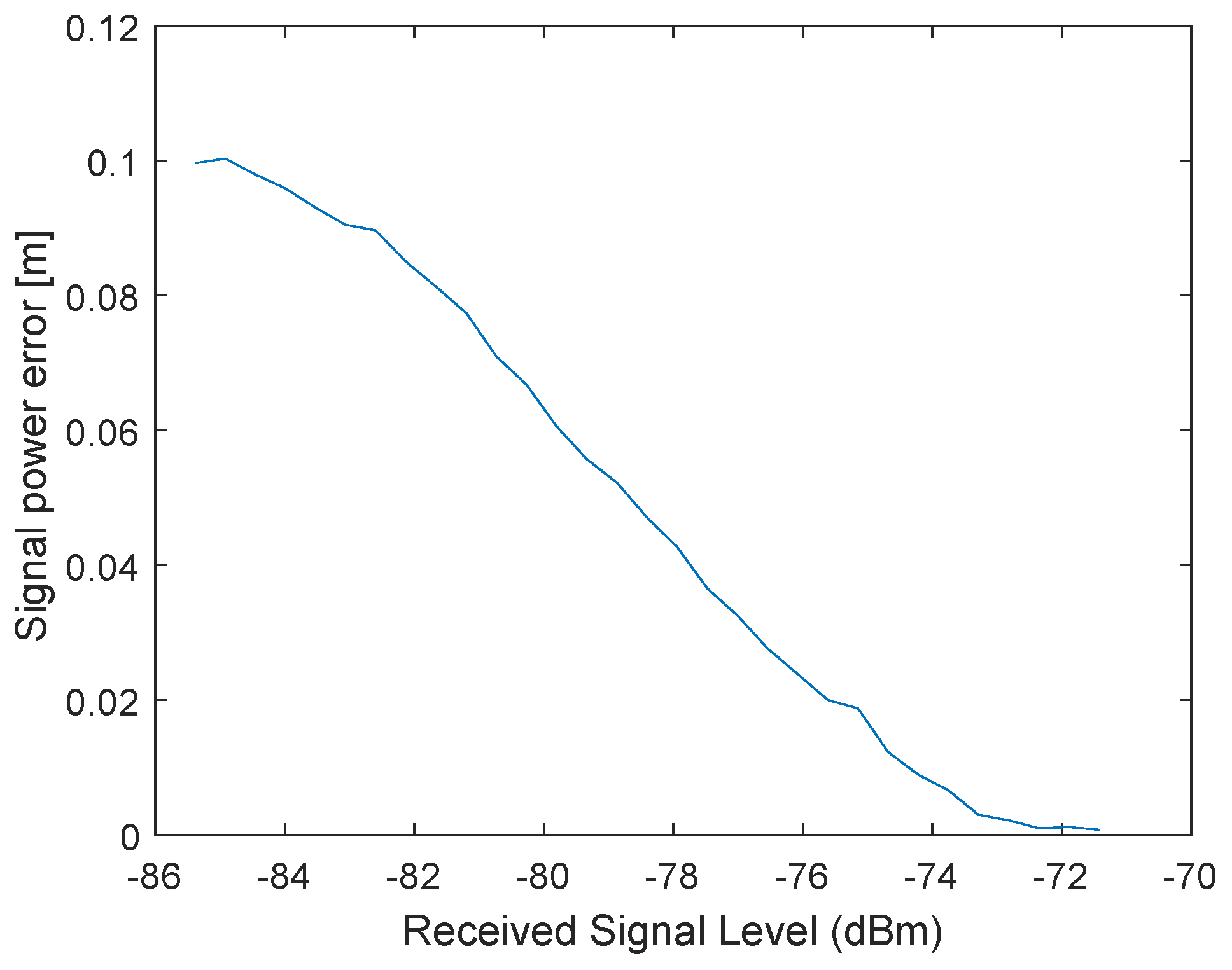
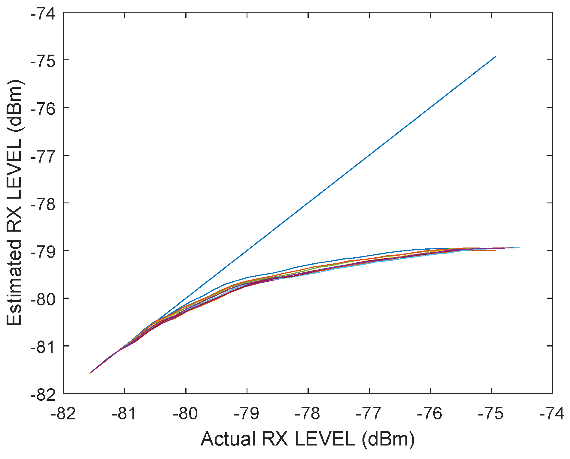
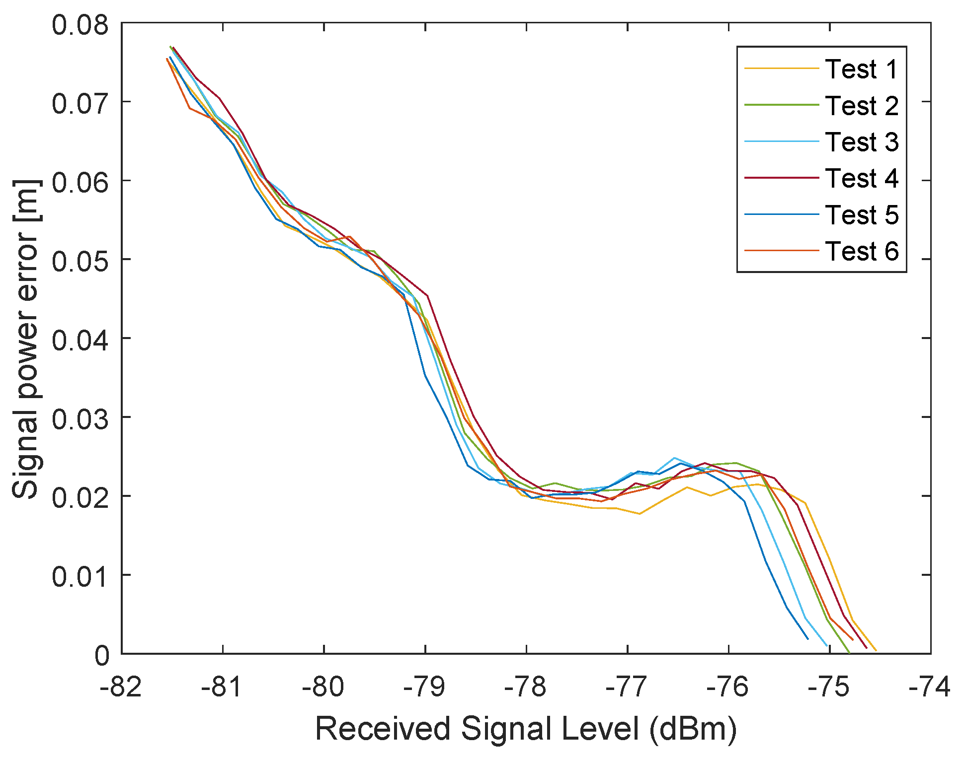
4. Signal Power Correction
4.1. General Approach
4.2. Proposed Approach for the Signal Power Correction
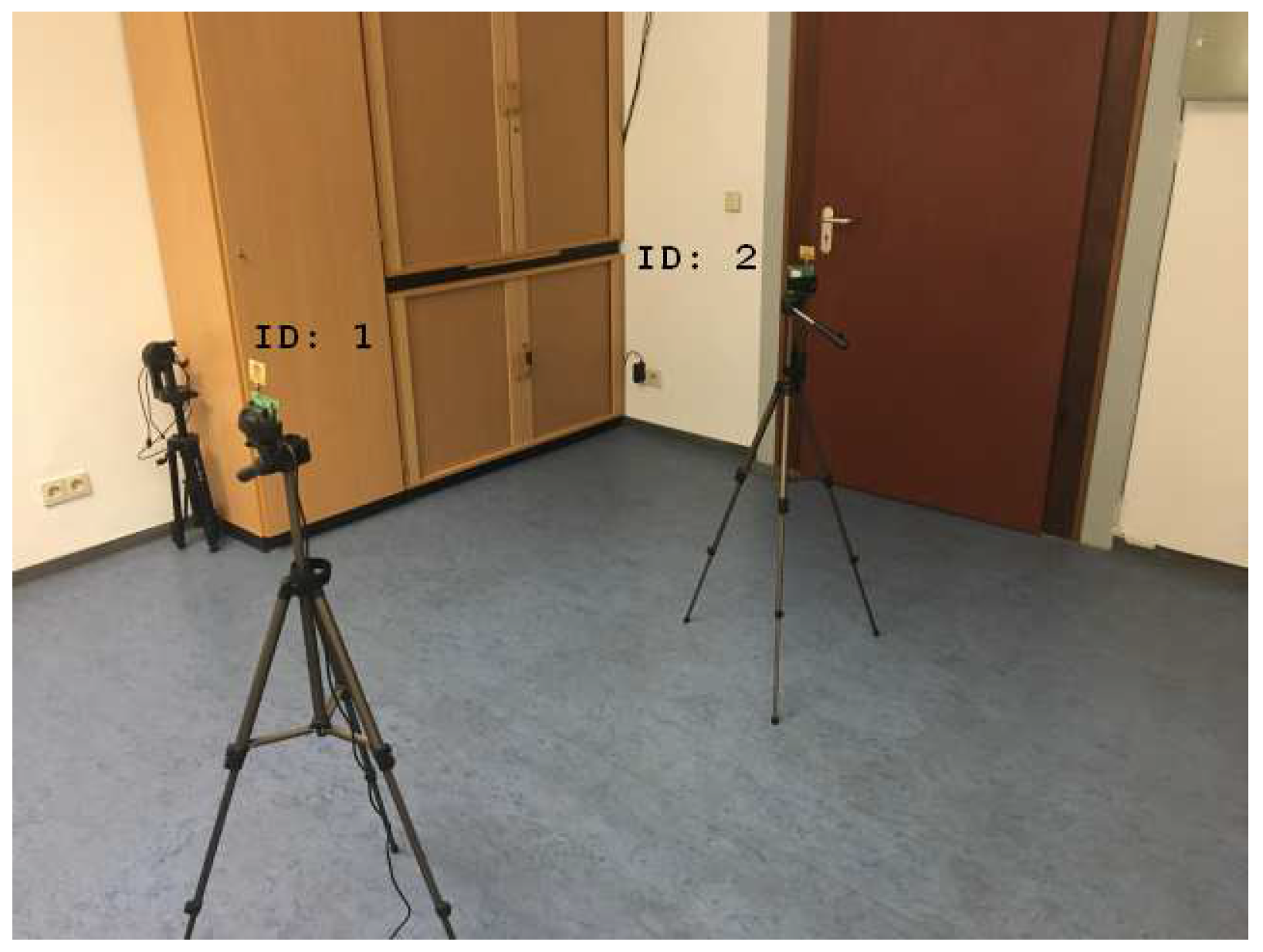
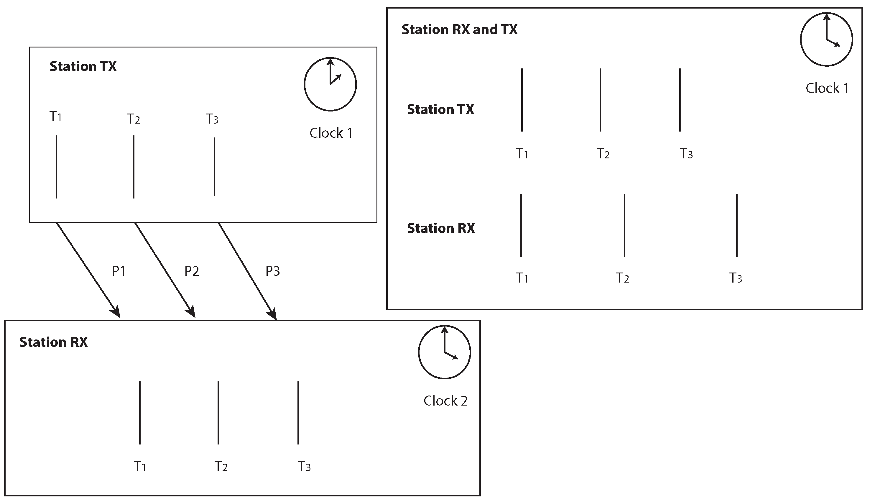
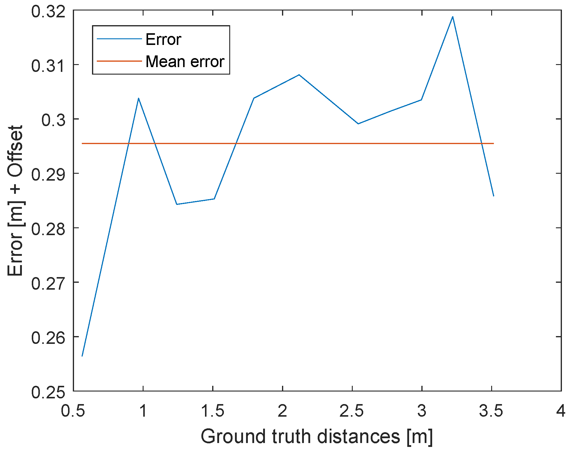
5. Two Way Ranging
6. Conclusions
7. Patents
Author Contributions
Funding
Conflicts of Interest
Abbreviations
| UWB | Ultra-wideband (UWB) |
| TOA | Time of Arrival (TOA) |
| PLL | Phase-locked loop |
| TWR | Two-way ranging |
| FMCW | Frequency modulated continuous wave |
| VCO | Voltage-controlled oscillator |
| VE | Received carrier frequency |
| VI | Internal loop frequency |
| PPM | Parts per million |
| TX | Transmitting station |
| RX | Receiving station |
| PRF | Pulse repetition frequency |
| RSSI | Received signal strength indication |
References
- Liu, C.; Wang, J.; Zhang, Z.; Bian, X.; Mei, X. SLAM for planar mobile robot. In Proceedings of the 2nd IEEE Advanced Information Management, Communicates, Electronic and Automation Control Conference (IM-CEC), Xi’an, China, 25–27 May 2018; pp. 1239–1242. [Google Scholar]
- Wang, Z.; Jia, Q.; Ye, P.; Sun, H. A depth camera based lightweight visual SLAM algorithm. In Proceedings of the 4th International Conference on Systems and Informatics (ICSAI), Hangzhou, China, 11–13 November 2017; pp. 143–148. [Google Scholar]
- Shen, X.; Yang, S.; He, J.; Huang, Z. Improved localization algorithm based on RSSI in low power bluetooth network. In Proceedings of the 2nd International Conference on Cloud Computing and Internet of Things (CCIOT), Dalian, China, 22–23 October 2016; pp. 134–137. [Google Scholar]
- Zhu, J.Y.; Xu, J.; Zheng, A.X.; He, J.; Wu, C.; Li, V.O.K. WIFI fingerprinting indoor localization system based on spatio-temporal (s-t) metrics. In Proceedings of the International Conference on Indoor Positioning and Indoor Navigation (IPIN), Busan, Korea, 27–30 October 2014; pp. 611–614. [Google Scholar]
- Resch, A.; Pfeil, R.; Wegener, M.; Stelzer, A. Review of the LPM local positioning measurement system. In Proceedings of the International Conference on Localization and GNSS, Starnberg, Germany, 25–27 June 2012; pp. 1–5. [Google Scholar]
- Zwirello, L.; Schipper, T.; Jalilvand, M.; Zwick, T. Realization limits of impulse-based localization system for large-scale indoor applications. IEEE Trans. Instrum. Meas. 2015, 64, 39–51. [Google Scholar] [CrossRef]
- Dotlic, I.; Connell, A.; Ma, H.; Clancy, J.; McLaughlin, M. Angle of arrival estimation using decawave DW1000 integrated circuits. In Proceedings of the 14th Workshop on Positioning, Navigation and Communications (WPNC), Bremen, Germany, 25–26 October 2017; pp. 1–6. [Google Scholar]
- Barua, B.; Kandil, N.; Hakem, N. On performance study of TWR UWB ranging in underground mine. In Proceedings of the Sixth International Conference on Digital Information, Networking, and Wireless Communications (DINWC), Beirut, Lebanon, 25–27 April 2018; pp. 28–31. [Google Scholar]
- Zhou, Y.; Law, C.L.; Guan, Y.L.; Chin, F. Indoor elliptical localization based on asynchronous UWB range measurement. IEEE Trans. Instrum. Meas. 2011, 60, 248–257. [Google Scholar] [CrossRef]
- Gerrits, J.F.M.; Farserotu, J.R.; Long, J.R. Multipath behavior of FM-UWB signals. In Proceedings of the IEEE International Conference on Ultra-Wideband, Singapore, 24–26 September 2007; pp. 162–167. [Google Scholar]
- Saeed, R.A.; Khatun, S.; Ali, B.M.; Khazani, M.A. Ultra-wideband (UWB) geolocation in NLOS multipath fading environments. In Proceedings of the 13th IEEE International Conference on Networks Jointly held with the 2005 IEEE 7th Malaysia International Conf on Communic, Kuala Lumpur, Malaysia, 16–18 November 2005; pp. 1068–1073. [Google Scholar]
- Ruiz, A.R.J.; Granja, F.S. Comparing ubisense, bespoon, and decawave UWB location systems: Indoor performance analysis. IEEE Trans. Instrum. Meas. 2017, 66, 2106–2117. [Google Scholar] [CrossRef]
- McElroy, C.; Neirynck, D.; McLaughlin, M. Comparison of wireless clock synchronization algorithms for indoor location systems. In Proceedings of the IEEE International Conference on Communications Workshops (ICC), Sydney, NSW, Australia, 10–14 June 2014; pp. 157–162. [Google Scholar]
- DECAWAVE. DW1000 User Manual, Version 2.15, p. 45. Available online: https://www.decawave.com (accessed on 3 July 2019).
- DECAWAVE. APS011 APPLICATION NOTE: Sources of Error in TWR Schemes, Version 1.0, p. 10. Available online: https://www.decawave.com (accessed on 3 July 2019).
- Fofana, N.I.; Van Den Bossche, A.; Dalcé, R.; Val, T. An original correction method for indoor ultra wide band rangingbased localisation system. In Ad-Hoc Mobile and Wireless Networks, Proceedings of the International Conference on Ad-Hoc Networks and Wireless, Lille, France, 4–6 July 2016; Springer: Berlin, Germany, 2016; Volume 9724, pp. 79–92. [Google Scholar]
- Van Den Bossche, A.; Dalce, R.; Fofana, N.I.; Val, T. DecaDuino: An ppen framework for wireless time-of-flight ranging systems. In Proceedings of the IFIP Wireless Days (WD), Toulouse, France, 23–25 March 2016; pp. 1–7. [Google Scholar]
- Martel, F.M.; Sidorenko, J.; Bodensteiner, C.; Arens, M. Augmented reality and UWB technology fusion: Localization of objects with head mounted displays. In Proceedings of the 31st International Technical Meeting of The Satellite Division of the Institute of Navigation (ION GNSS+), Miami, FL, USA, 24–28 September 2018; pp. 685–692. [Google Scholar]
- Dotlic, I.; Connell, A.; McLaughlin, M. Ranging methods utilizing carrierfrequency offset estimation. In Proceedings of the 15th Workshop on Positioning, Navigation and Communications (WPNC), Bremen, Germany, 25–26 October 2018; pp. 1–6. [Google Scholar]
- Haluza, M.; Vesely, J. Analysis of signals from the DecaWave TREK1000 wideband positioning system using AKRS system. In Proceedings of the International Conference on Military Technologies (ICMT), Brno, Czech Republic, 31 May–2 June 2017; pp. 424–429. [Google Scholar]

| Parameter | Value |
|---|---|
| Center Frequency | 3993.6 MHz |
| Bandwidth | 499.2 MHz |
| Pulse repetition frequency | 64 MHz |
| Preamble length | 128 |
| Data rate | 6.81 Mbps |
| Notations | Definition |
|---|---|
| Timestamp | |
| Clock drift with respect to the timestamps n and m | |
| Timestamp error due to signal power | |
| Z | Hardware delay and signal power correction offset |
© 2019 by the authors. Licensee MDPI, Basel, Switzerland. This article is an open access article distributed under the terms and conditions of the Creative Commons Attribution (CC BY) license (http://creativecommons.org/licenses/by/4.0/).
Share and Cite
Sidorenko, J.; Schatz, V.; Scherer-Negenborn, N.; Arens, M.; Hugentobler, U. Decawave UWB Clock Drift Correction and Power Self-Calibration. Sensors 2019, 19, 2942. https://doi.org/10.3390/s19132942
Sidorenko J, Schatz V, Scherer-Negenborn N, Arens M, Hugentobler U. Decawave UWB Clock Drift Correction and Power Self-Calibration. Sensors. 2019; 19(13):2942. https://doi.org/10.3390/s19132942
Chicago/Turabian StyleSidorenko, Juri, Volker Schatz, Norbert Scherer-Negenborn, Michael Arens, and Urs Hugentobler. 2019. "Decawave UWB Clock Drift Correction and Power Self-Calibration" Sensors 19, no. 13: 2942. https://doi.org/10.3390/s19132942
APA StyleSidorenko, J., Schatz, V., Scherer-Negenborn, N., Arens, M., & Hugentobler, U. (2019). Decawave UWB Clock Drift Correction and Power Self-Calibration. Sensors, 19(13), 2942. https://doi.org/10.3390/s19132942