
Mach-Zehnder Interferometer Biochemical Sensor Based on Silicon-on-Insulator Rib Waveguide with Large Cross Section


Abstract
:1. Introduction
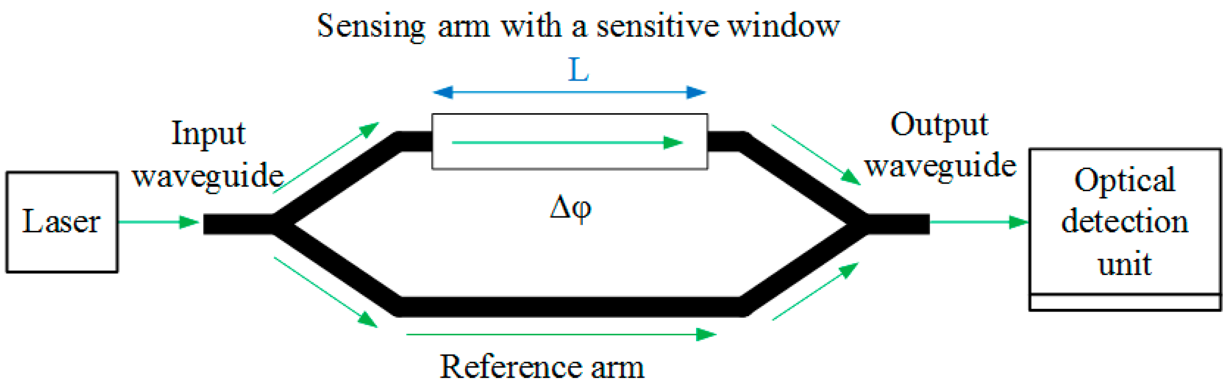
2. Principle of Operation
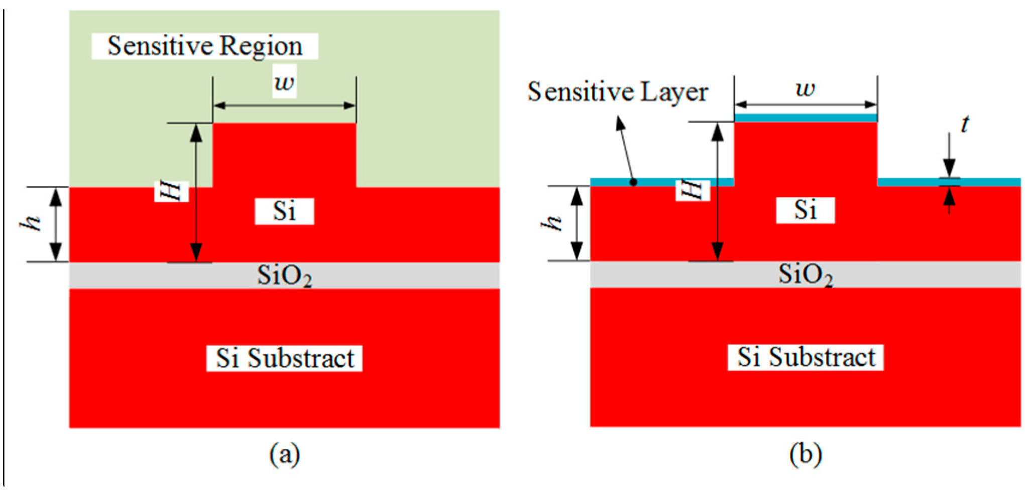
3. Section Dimensions of SOI Rib Waveguide
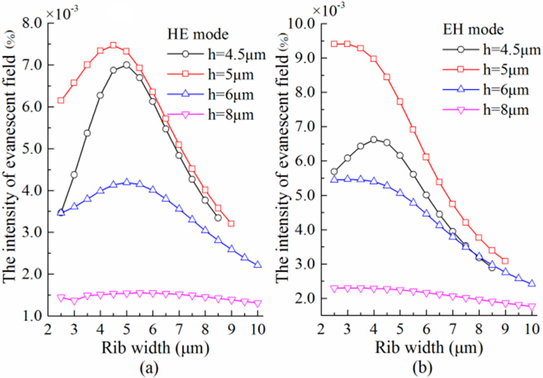
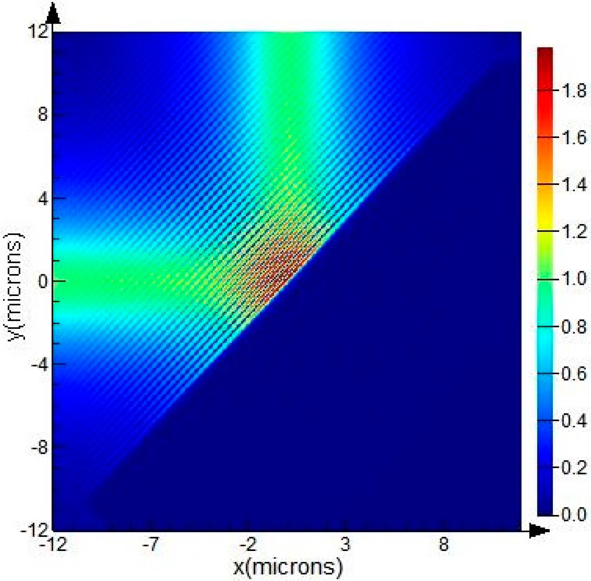
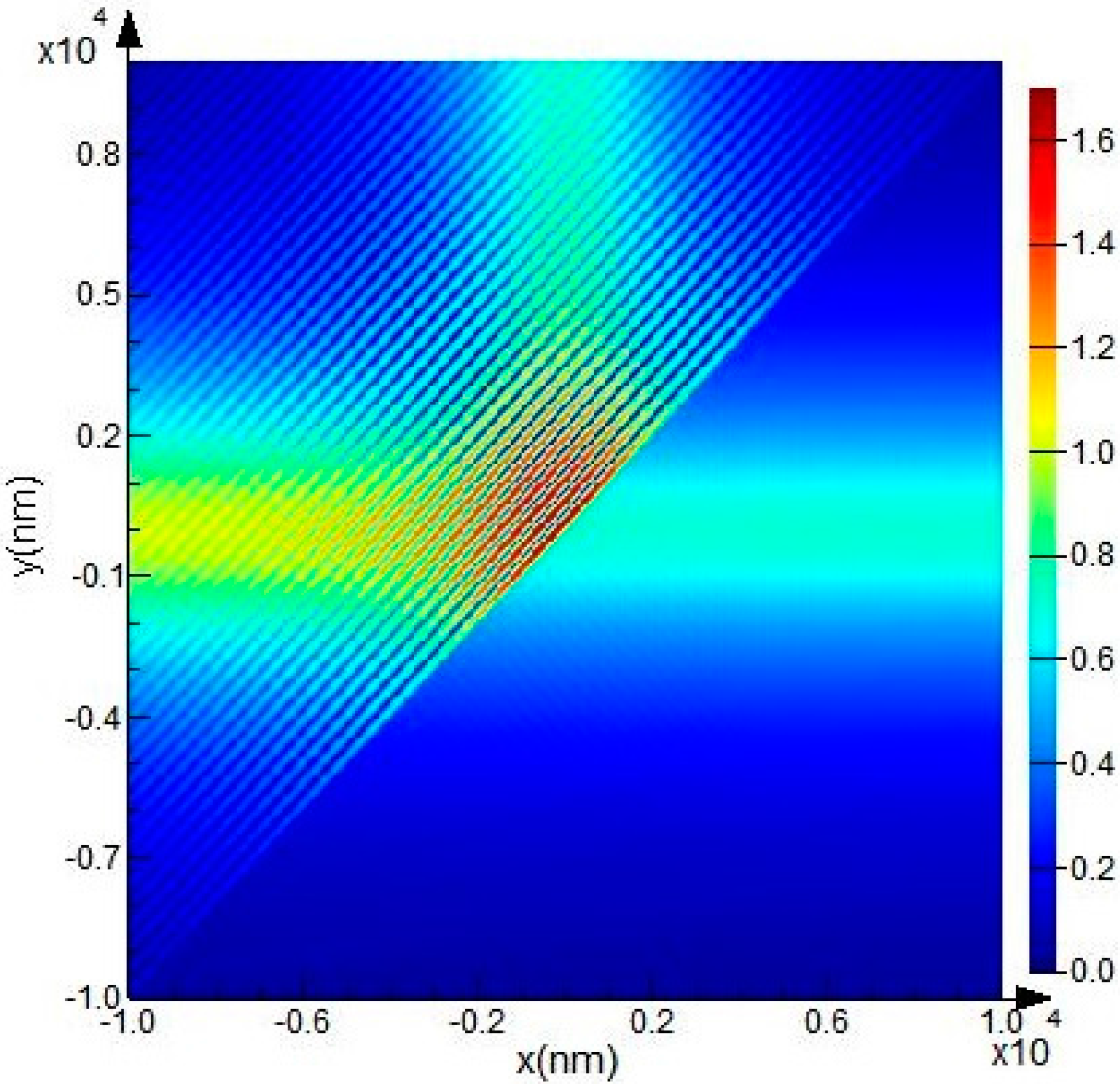
3.1. Intensity of Evanescent Field
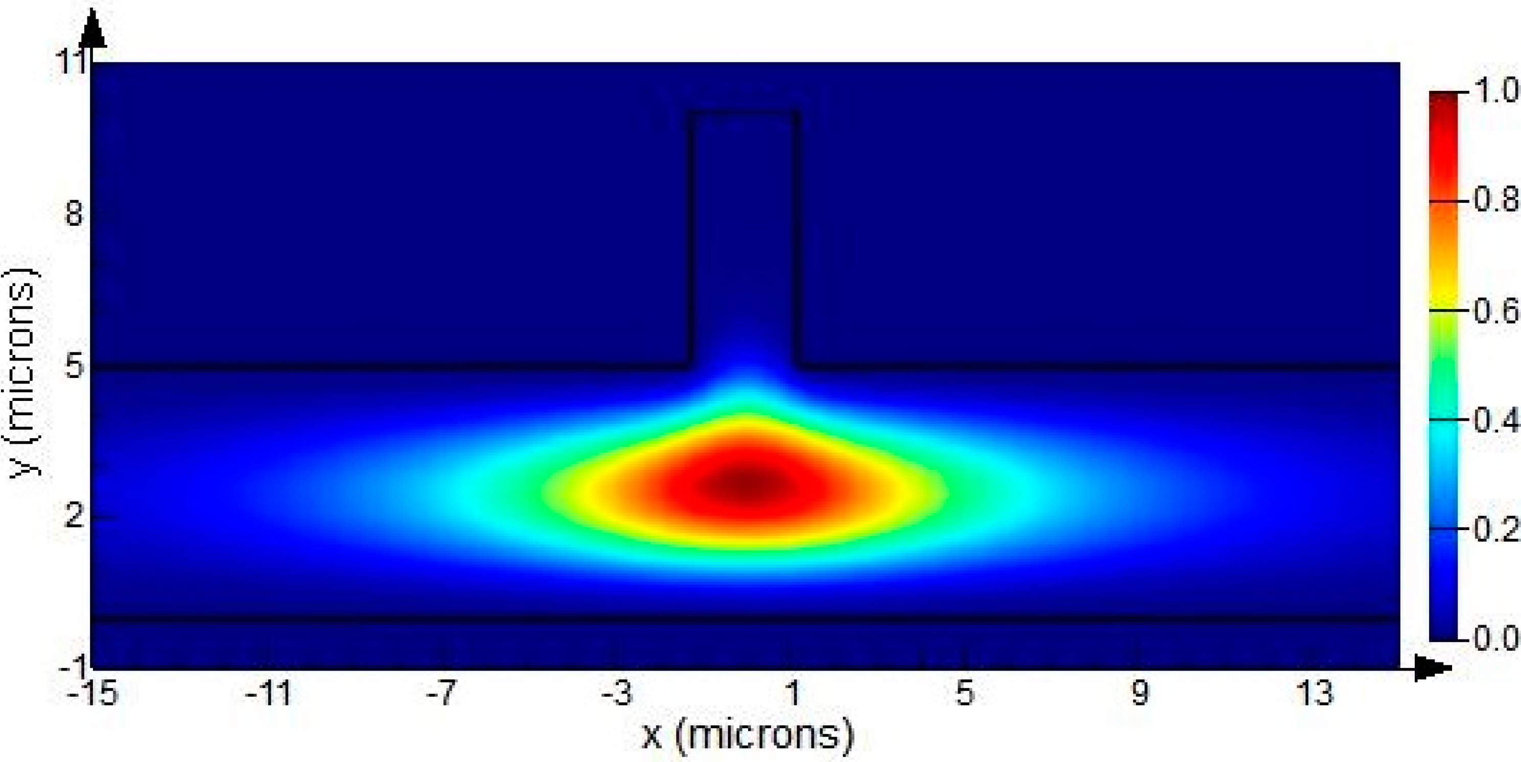
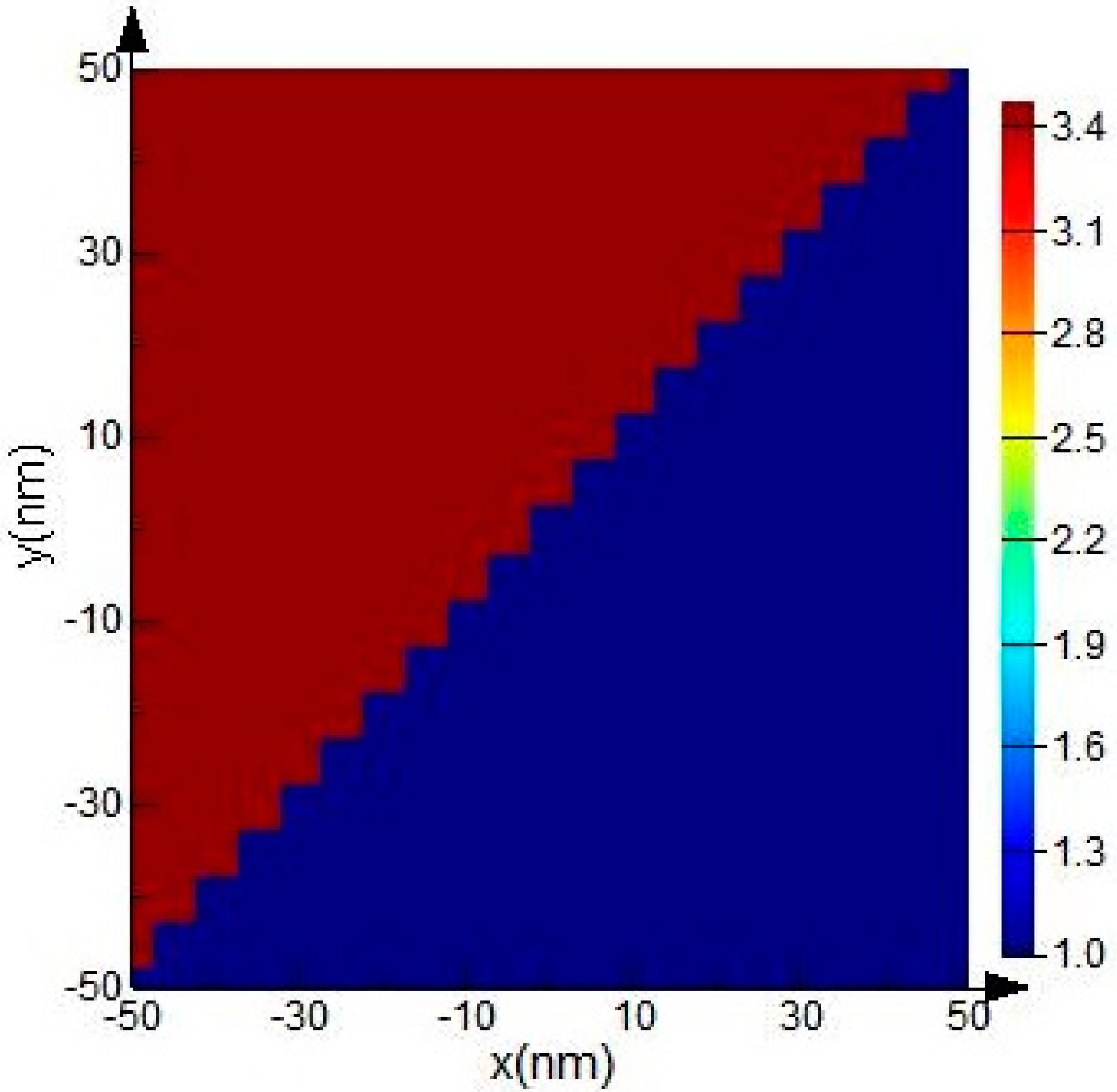
3.2. Optimization of Waveguide Section Dimensions


4. MZI Structure Implementation
4.1. Conventional Implementations

| Structure Type | Technology Platform | Technical Parameters & Requirements |
|---|---|---|
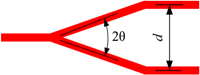 Y-junction | Mode-matching | When d = 50 μm, 2θ = 0.4°, The minimum length of a single branch: L0 = 7.2 mm. |
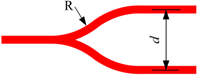 S-bend splitter | Waveguide bending | When d = 50 μm, R > 0.26 m, The minimum length of a single branch: L0 = 5.1 mm. |
 Multimode interference | Self-imaging effect [19] | When d = 50 μm, The minimum length of a single branch: L0 > 12 mm. |
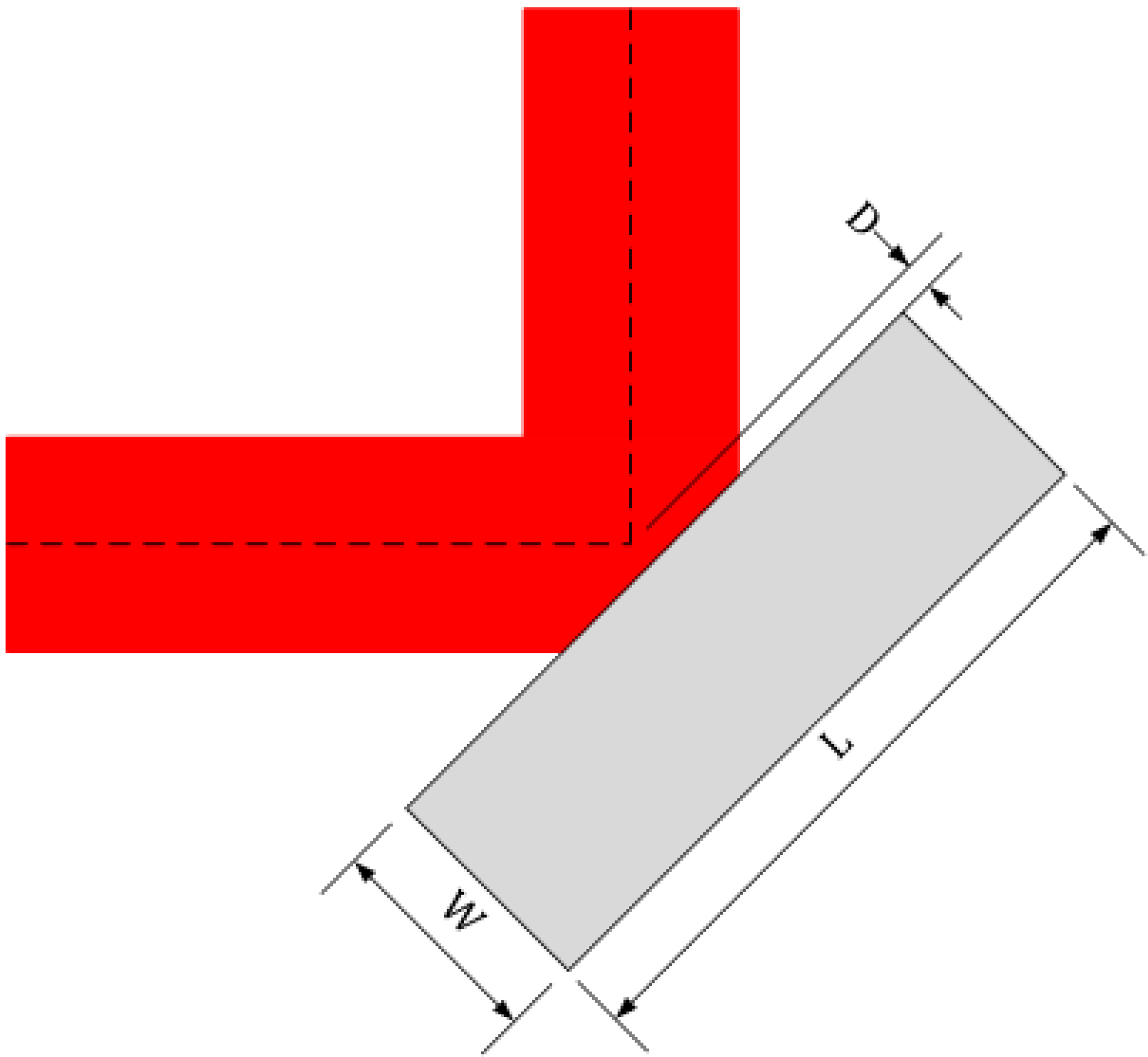
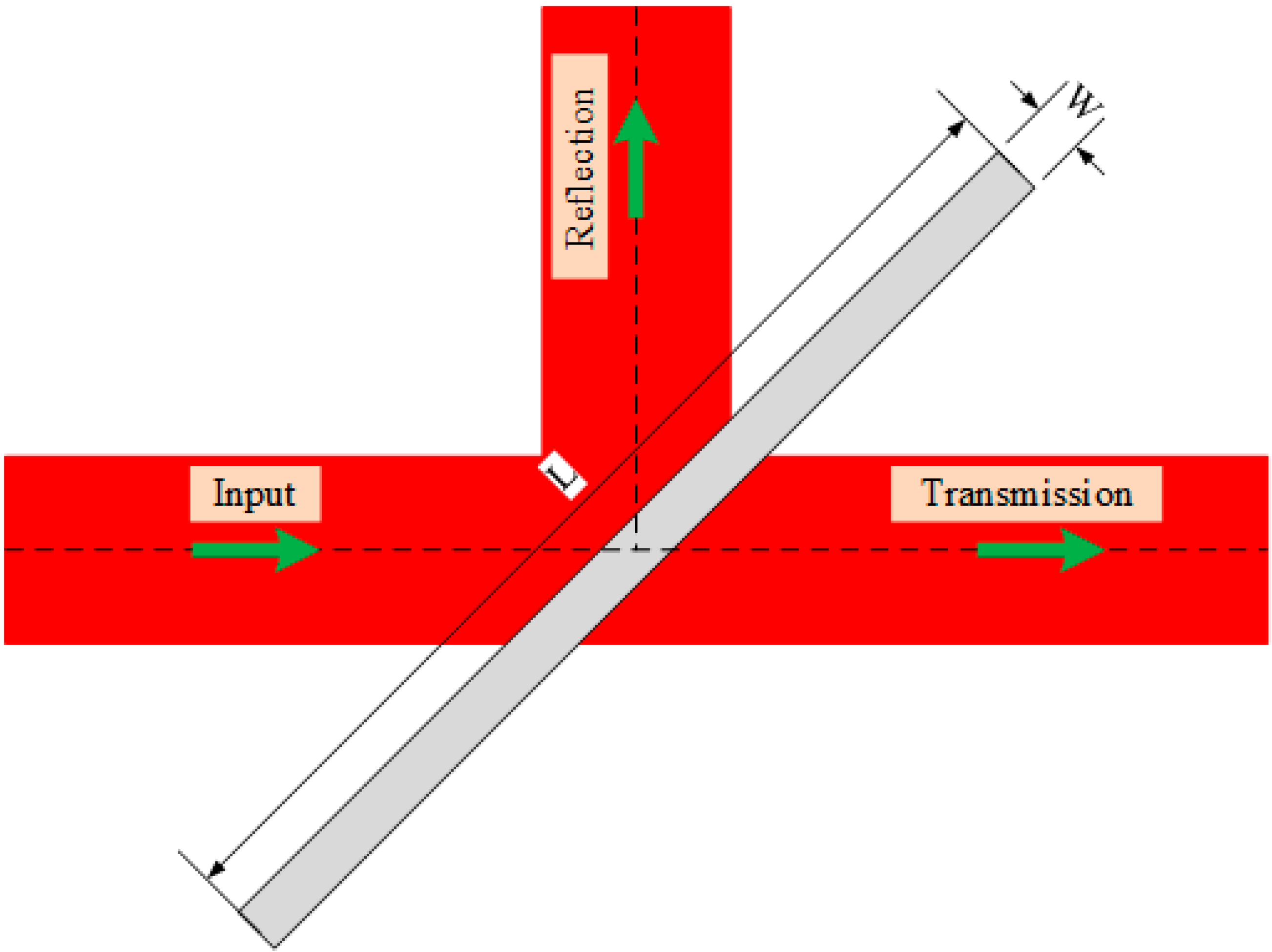
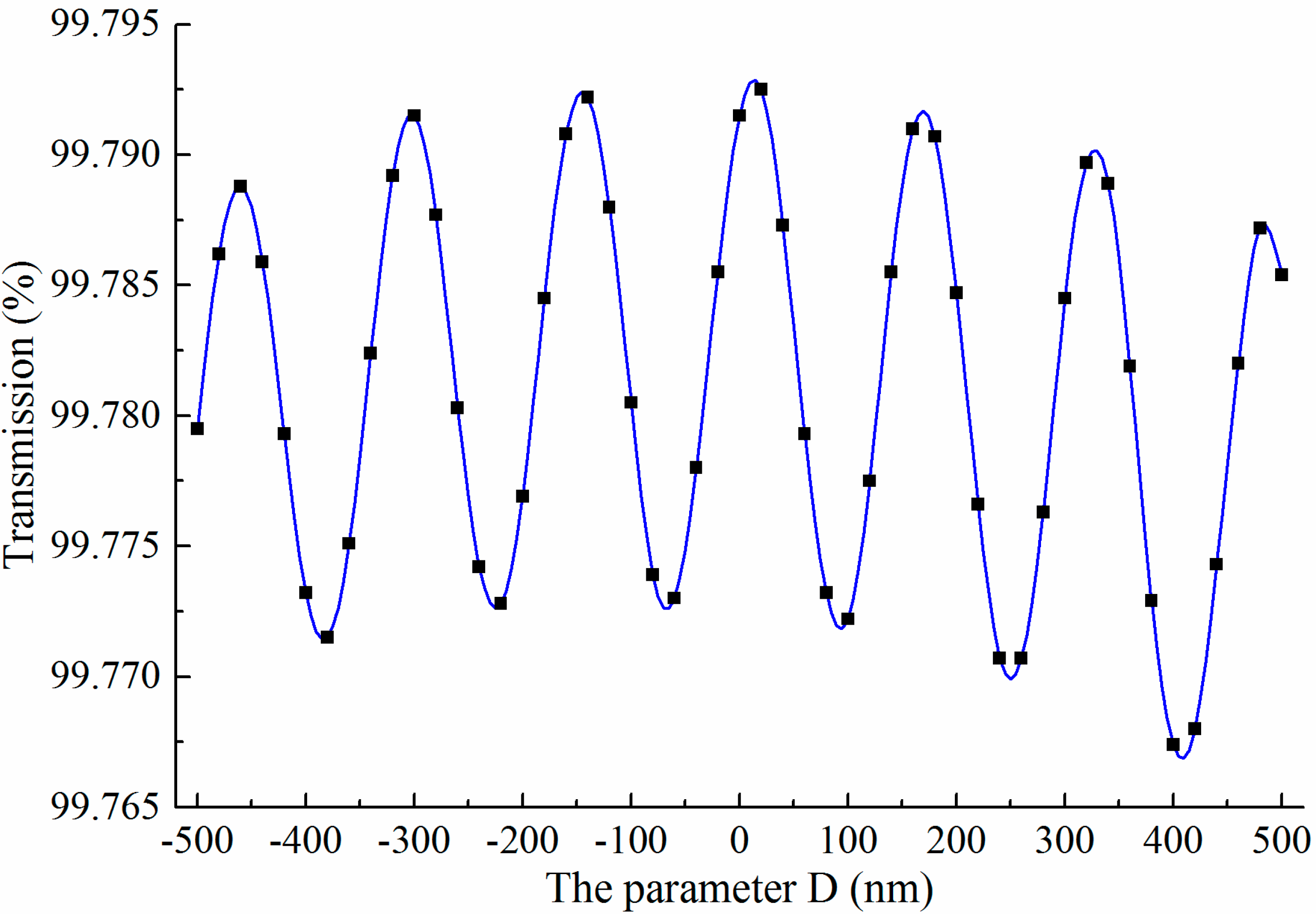
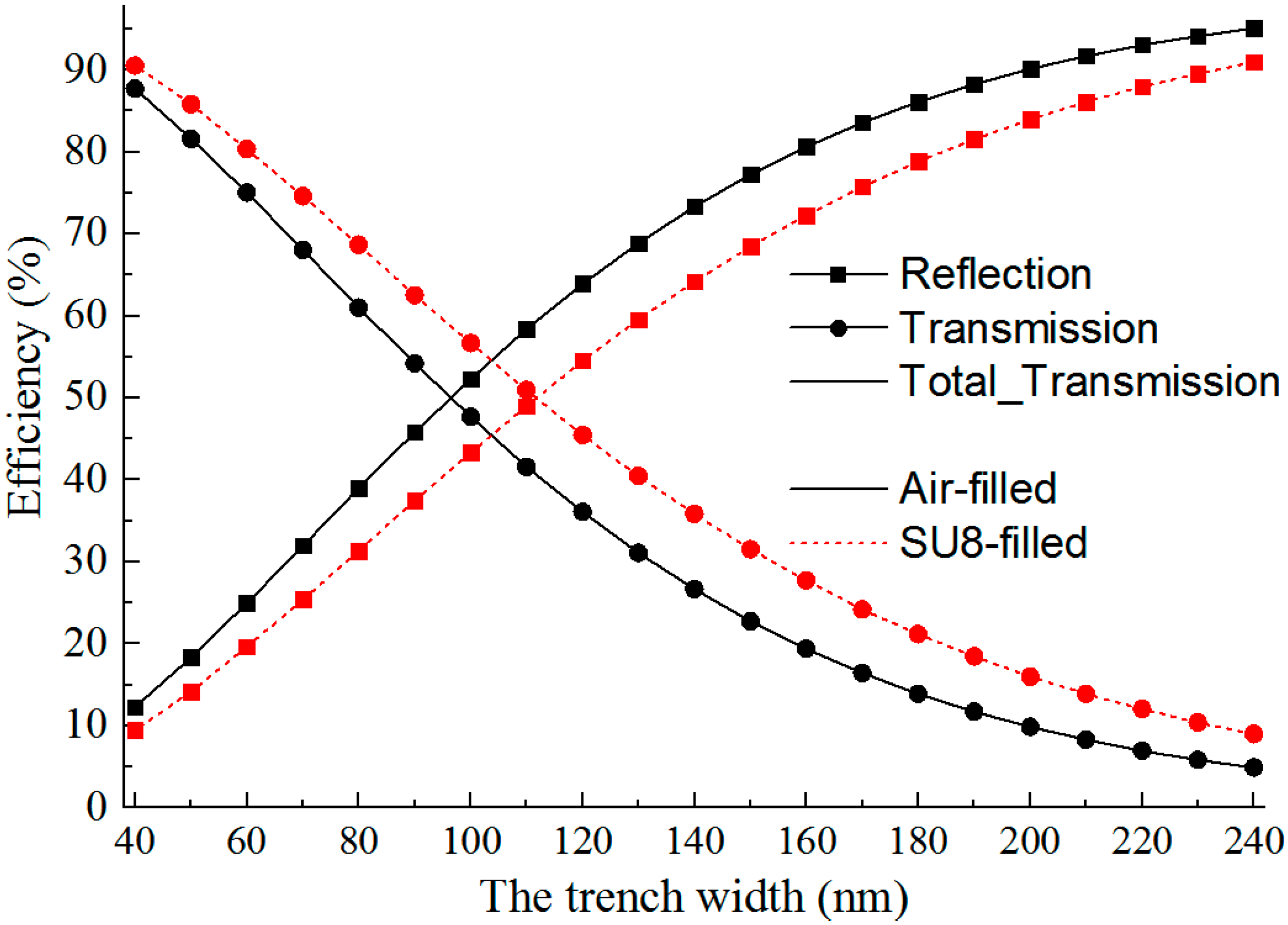
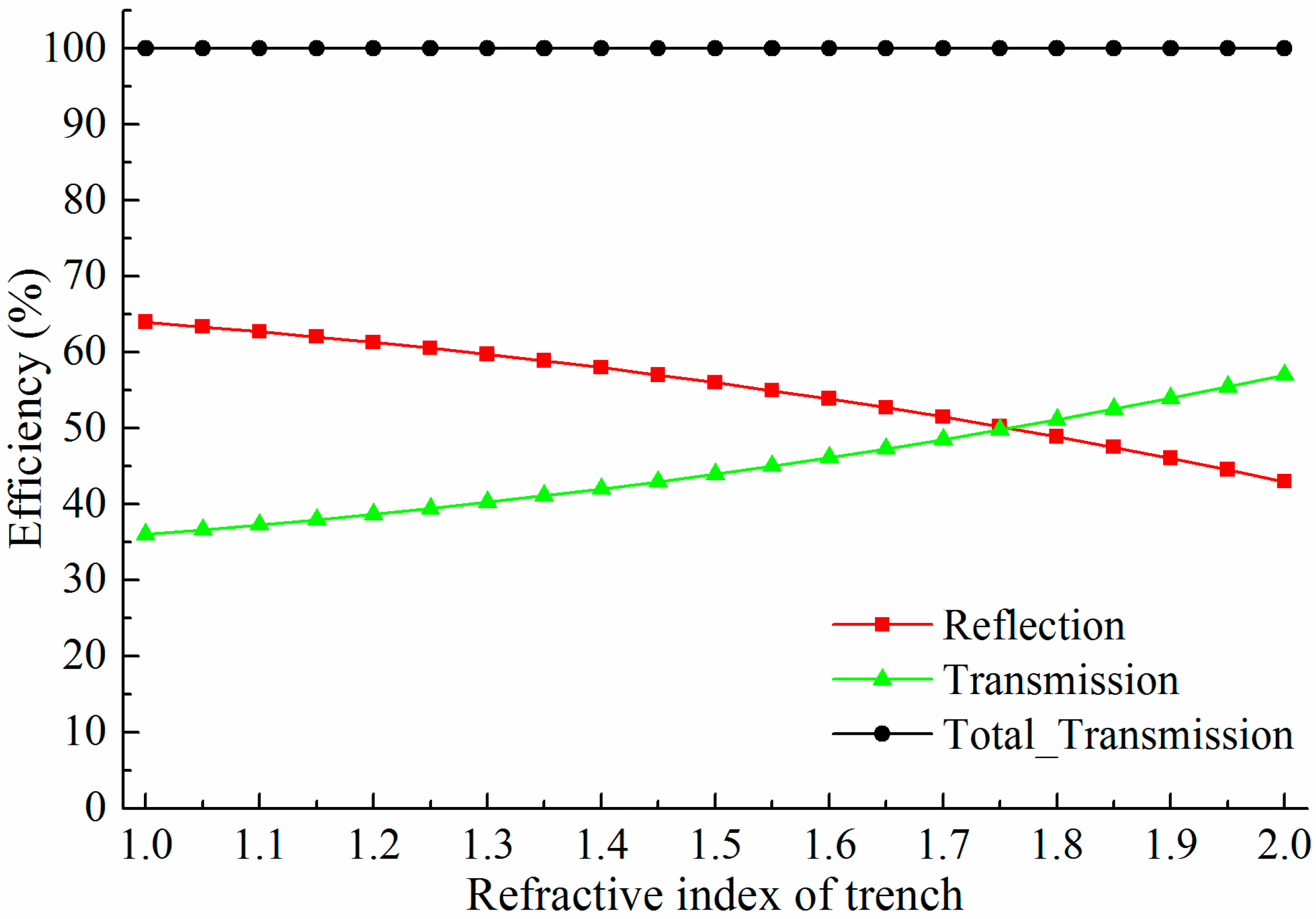
4.2. Trench-Based Bend and Branch


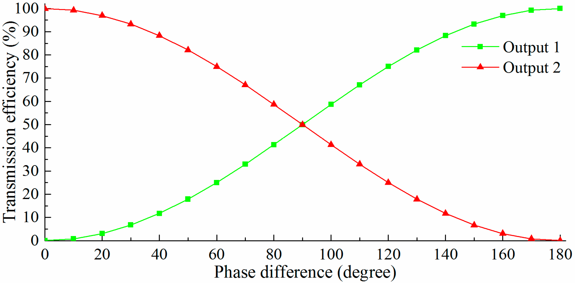
4.3. Proposed MZI Structure
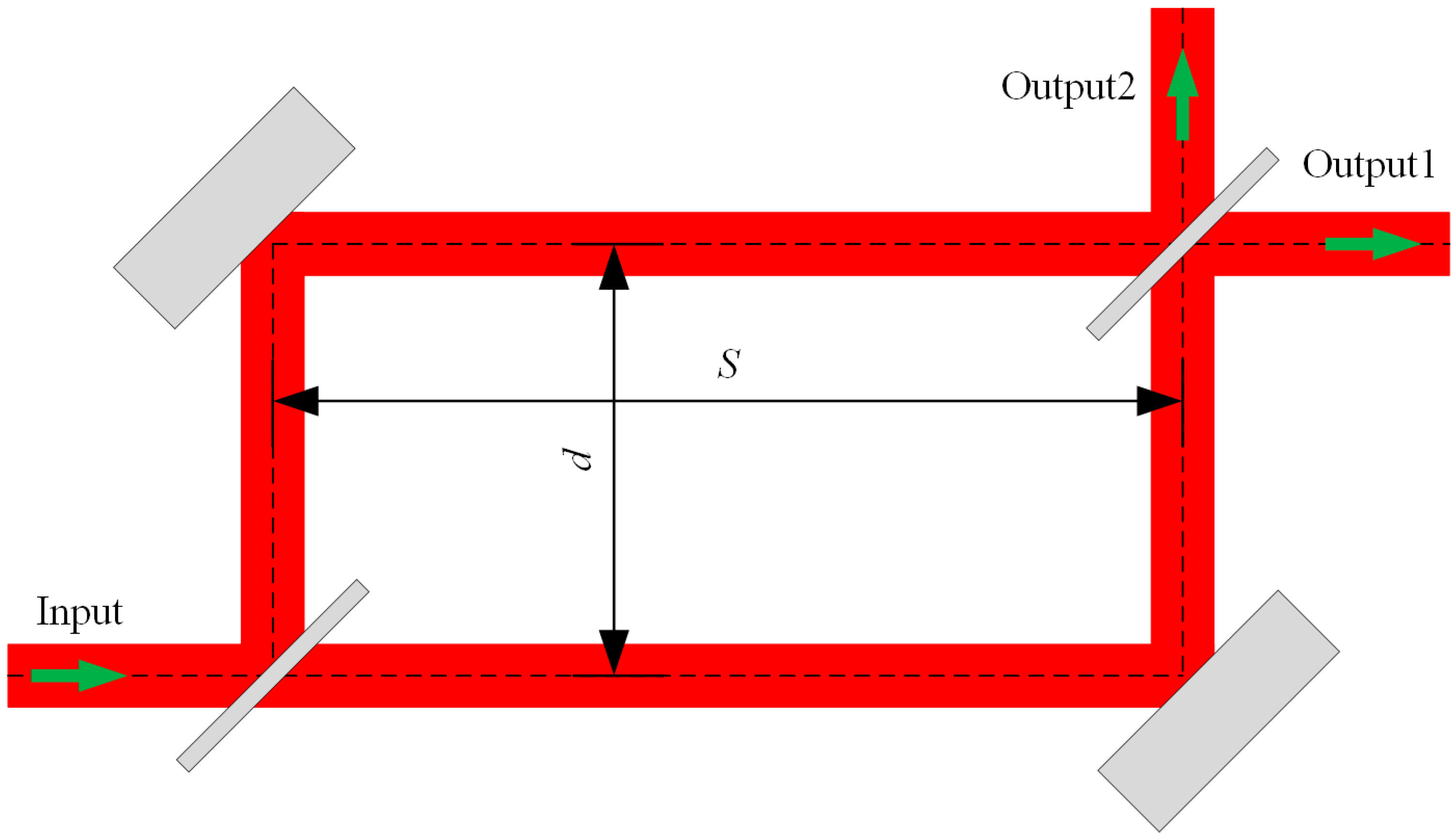
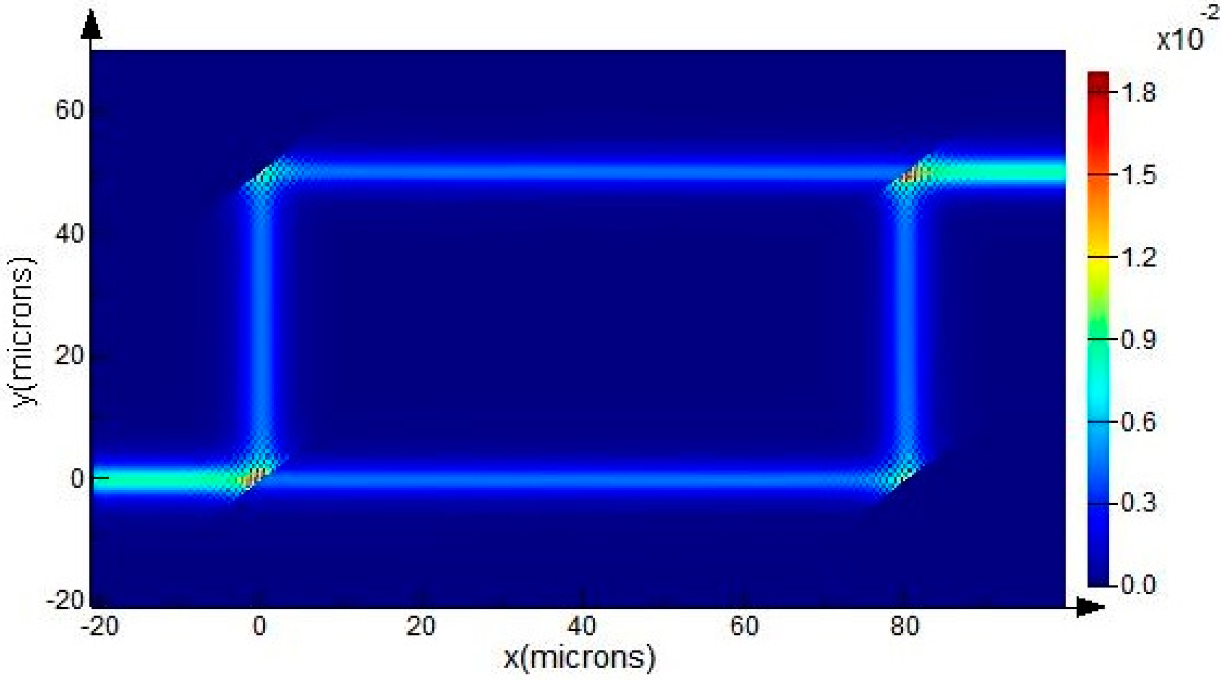
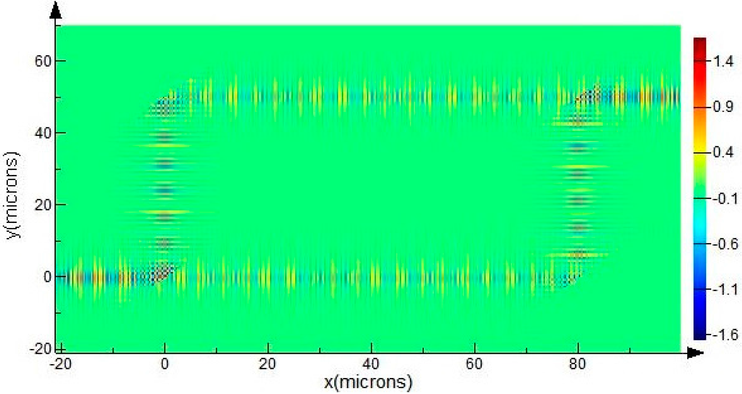


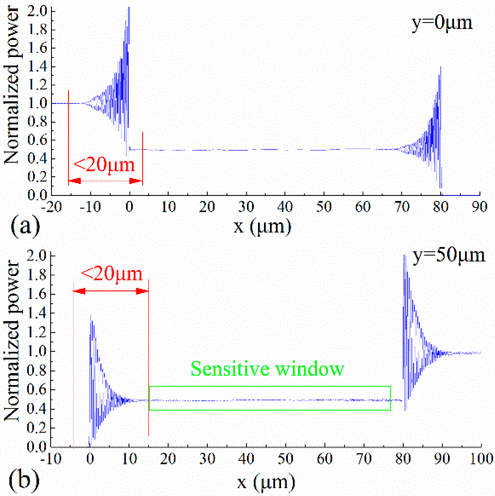
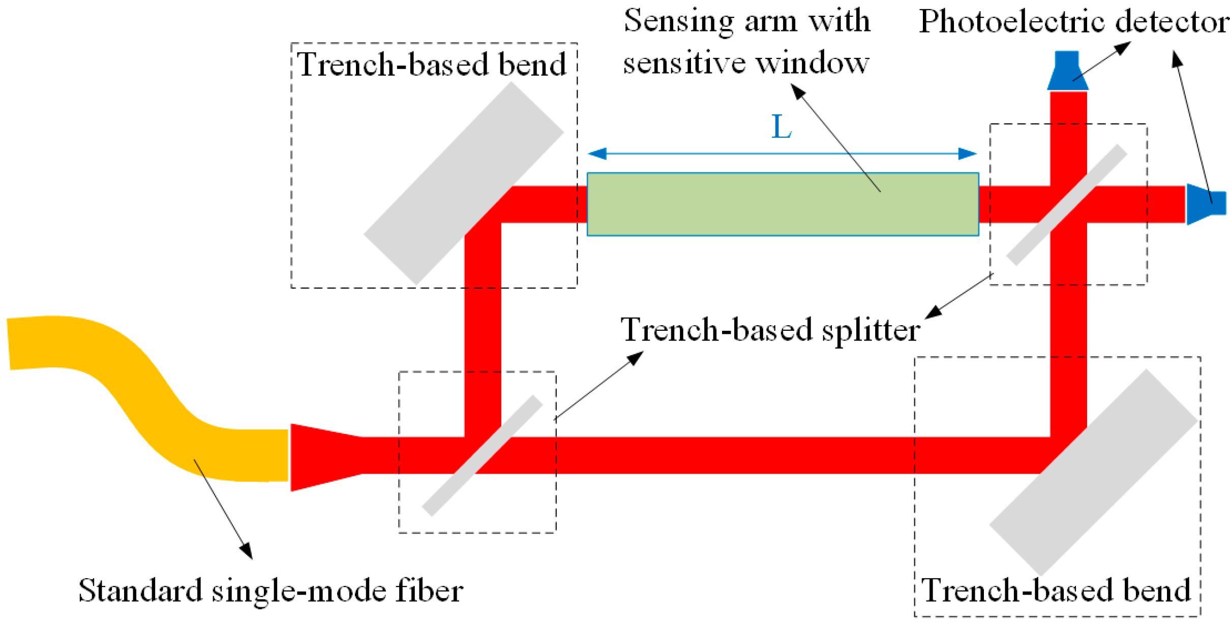
5. MZI Sensing Platform

6. Discussion
7. Conclusions
Acknowledgments
Author Contributions
Conflicts of Interest
References
- Hong, J.; Choi, J.S.; Han, G.; Kang, J.K.; Kim, C.; Kim, T.S.; Yoon, D.S. A Mach-Zehnder interferometer based on silicon oxides for biosensor applications. Anal. Chim. Acta. 2006, 573–574, 97–103. [Google Scholar] [CrossRef] [PubMed]
- Yalcin, A.; Popat, K.C.; Aldridge, J.C.; Desai, T.A.; Hryniewicz, J.; Chbouki, N.; Little, B.E.; King, O.; Van, V.; Chu, S.; et al. Optical sensing of biomolecules using microring resonators. IEEE J. Sel. Top. Quant. 2006, 12, 148–155. [Google Scholar] [CrossRef]
- De Vos, K.; Bartolozzi, I.; Schacht, E.; Bienstman, P.; Baets, R. Silicon-on-Insulator microring resonator for sensitive and label-free biosensing. Opt. Express 2007, 15, 7610–7615. [Google Scholar]
- Claes, T.; Molera, J.G.; de Vos, K.; Schacht, E.; Baets, R.; Bienstman, P. Label-free biosensing with a slot-waveguide-based ring resonator in silicon on insulator. IEEE Photonics J. 2009, 1, 197–204. [Google Scholar] [CrossRef]
- Qi, Z.; Matsuda, N.; Itoh, K.; Murabayashi, M.; Lavers, C.R. A design for improving the sensitivity of a Mach-Zehnder interferometer to chemical and biological measurands. Sens. Actuators B Chem. 2002, 81, 254–258. [Google Scholar] [CrossRef]
- Irawan, D.; Saktioto, T.; Ali, J.; Yupapin, P. Design of Mach-Zehnder interferometer and ring resonator for biochemical sensing. Photonics Sens. 2015, 5, 12–18. [Google Scholar] [CrossRef]
- Fan, X.; White, I.M.; Shopova, S.I.; Zhu, H.; Suter, J.D.; Sun, Y. Sensitive optical biosensors for unlabeled targets: A review. Anal. Chim. Acta. 2008, 620, 8–26. [Google Scholar] [CrossRef] [PubMed]
- Liu, Q.; Tu, X.; Kim, K.W.; Kee, J.S.; Shin, Y.; Han, K.; Yoon, Y.; Lo, G.; Park, M.K. Highly sensitive Mach-Zehnder interferometer biosensor based on silicon nitride slot waveguide. Sens. Actuators B Chem. 2013, 188, 681–688. [Google Scholar] [CrossRef]
- Densmore, A.; Xu, D.X.; Waldron, P.; Janz, S.; Cheben, P.; Lapointe, J.; Delâge, A.; Lamontagne, B.; Schmid, J.H.; Post, E. A silicon-on-insulator photonic wire based evanescent field sensor. IEEE Photonics Technol. Lett. 2006, 18, 2520–2522. [Google Scholar] [CrossRef]
- Densmore, A.; Xu, D.X.; Janz, S.; Waldron, P.; Mischki, T.; Lopinski, G.; Delâge, A.; Lapointe, J.; Cheben, P.; Schmid, J.H.; et al. Spiral-path high-sensitivity silicon photonic wire molecular sensor with temperature-independent response. Opt. Lett. 2008, 33, 596–598. [Google Scholar] [CrossRef] [PubMed]
- Barrios, C.A.; Gylfason, K.B.; Sanchez, B.; Griol, A.; Sohlstrom, H.; Holgado, M.; Casquel, R. Slot-waveguide biochemical sensor. Opt. Lett. 2007, 32, 3080–3082. [Google Scholar] [CrossRef] [PubMed]
- Barrios, C.A.; Banuls, M.J.; Gonzalez-Pedro, V.; Gylfason, K.B.; Sanchez, B.; Griol, A.; Maquieira, A.; Sohlstrom, H.; Holgado, M.; Casquel, R. Label-free optical biosensing with slot-waveguides. Opt. Lett. 2008, 33, 708–710. [Google Scholar] [CrossRef] [PubMed]
- Soref, R.A.; Schmidtchen, J.; Petermann, K. Large single-mode rib waveguides in GeSi-Si and Si-on-SiO2. IEEE J. Quantum Electron. 1991, 27, 1971–1974. [Google Scholar] [CrossRef]
- Chao, C.; Fung, W.; Guo, L.J. Polymer microring resonators for biochemical sensing applications. IEEE J. Select. Top. Quantum Electron. 2006, 12, 134–142. [Google Scholar] [CrossRef]
- Dell'Olio, F.; Passaro, V.M. Optical sensing by optimized silicon slot waveguides. Opt. Express 2007, 15, 4977–4993. [Google Scholar] [CrossRef] [PubMed]
- Reed, G.T.; Knights, A.P. Silicon-On-Insulator (SOI) Photonics. In Silicon Photonics: An Introduction; John Wiley & Sons, Ltd.: Chichester, UK, 2004. [Google Scholar]
- Pogossian, S.P.; Vescan, L.; Vonsovici, A. The single-mode condition for semiconductor rib waveguides with large cross section. J. Lightwave Technol. 1998, 16, 1851–1853. [Google Scholar] [CrossRef]
- Zhu, Z.; Brown, T. Full-vectorial finite-difference analysis of microstructured optical fibers. Opt. Express 2002, 10, 853–864. [Google Scholar] [CrossRef] [PubMed]
- Wei, H.; Yu, J.; Zhang, X.; Liu, Z. Compact 3-dB tapered multimode interference coupler in silicon-on-insulator. Opt. Express 2001, 26, 878–880. [Google Scholar] [CrossRef]
- Tang, Y.Z.; Wang, W.H.; Li, T.; Wang, Y.L. Integrated waveguide turning mirror in silicon-on-insulator. IEEE Photonics Technol. Lett. 2002, 14, 68–70. [Google Scholar] [CrossRef]
- Lardenois, S.; Pascal, D.; Vivien, L.; Cassan, E.; Laval, S.; Orobtchouk, R.; Heitzmann, M.; Bouzaida, N.; Mollard, L. Low-loss submicrometer silicon-on-insulator rib waveguides and corner mirrors. Opt. Lett. 2003, 28, 1150–1152. [Google Scholar] [CrossRef] [PubMed]
- Kiyat, I.; Aydinli, A.; Dagli, N. A compact silicon-on-insulator polarization splitter. IEEE Photonics Technol. Lett. 2005, 17, 100–102. [Google Scholar] [CrossRef]
- Qian, Y.; Kim, S.; Song, J.; Nordin, G.P.; Jiang, J. Compact and low loss silicon-on-insulator rib waveguide 90° bend. Opt. Express 2006, 14, 6020–6028. [Google Scholar] [CrossRef] [PubMed]
- Qian, Y.; Song, J.; Kim, S.; Nordin, G.P. Compact 90° trench-based splitter for silicon-on-insulator rib waveguides. Opt. Express 2007, 15, 16712–16718. [Google Scholar] [CrossRef] [PubMed]
- Lau, S.T.; Ballantyne, J.M. Two-dimensional analysis of a dielectric waveguide mirror. J. Lightwave Technol. 1997, 15, 551–558. [Google Scholar] [CrossRef]
- Berenger, J. A perfectly matched layer for the absorption of electromagnetic waves. J. Comput. Phys. 1994, 114, 185–200. [Google Scholar] [CrossRef]
- Cai, J.; Nordin, G.P.; Kim, S.; Jiang, J. Three-dimensional analysis of a hybrid photonic crystal-conventional waveguide 90 degree bend. Appl. Opt. 2004, 43, 4244–4249. [Google Scholar] [CrossRef] [PubMed]
- Prieto, F.; Sepulveda, B.; Calle, A.; Llobera, A.; Domínguez, C.; Abad, A.; Montoya, A.; Lechuga, L.M. An integrated optical interferometric nanodevice based on silicon technology for biosensor applications. Nanotechnology 2003, 14. [Google Scholar] [CrossRef]
- Heideman, R.G.; Lambeck, P.V. Remote opto-chemical sensing with extreme sensitivity: Design, fabrication and performance of a pigtailed integrated optical phase-modulated Mach-Zehnder interferometer system. Sens. Actuators B Chem. 1999, 61, 100–127. [Google Scholar] [CrossRef]
- Zinoviev, K.; Carrascosa, L.G.; Sánchez Del Río, J.; Sepúlveda, B.; Domínguez, C.; Lechuga, L.M. Silicon photonic biosensors for lab-on-a-chip applications. Adv. Opt. Technol. 2008, 2008, 1–6. [Google Scholar] [CrossRef]
© 2015 by the authors; licensee MDPI, Basel, Switzerland. This article is an open access article distributed under the terms and conditions of the Creative Commons Attribution license (http://creativecommons.org/licenses/by/4.0/).
Share and Cite
Yuan, D.; Dong, Y.; Liu, Y.; Li, T. Mach-Zehnder Interferometer Biochemical Sensor Based on Silicon-on-Insulator Rib Waveguide with Large Cross Section. Sensors 2015, 15, 21500-21517. https://doi.org/10.3390/s150921500
Yuan D, Dong Y, Liu Y, Li T. Mach-Zehnder Interferometer Biochemical Sensor Based on Silicon-on-Insulator Rib Waveguide with Large Cross Section. Sensors. 2015; 15(9):21500-21517. https://doi.org/10.3390/s150921500
Chicago/Turabian StyleYuan, Dengpeng, Ying Dong, Yujin Liu, and Tianjian Li. 2015. "Mach-Zehnder Interferometer Biochemical Sensor Based on Silicon-on-Insulator Rib Waveguide with Large Cross Section" Sensors 15, no. 9: 21500-21517. https://doi.org/10.3390/s150921500
APA StyleYuan, D., Dong, Y., Liu, Y., & Li, T. (2015). Mach-Zehnder Interferometer Biochemical Sensor Based on Silicon-on-Insulator Rib Waveguide with Large Cross Section. Sensors, 15(9), 21500-21517. https://doi.org/10.3390/s150921500