C59N Peapods Sensing the Temperature

Abstract
:1. Introduction
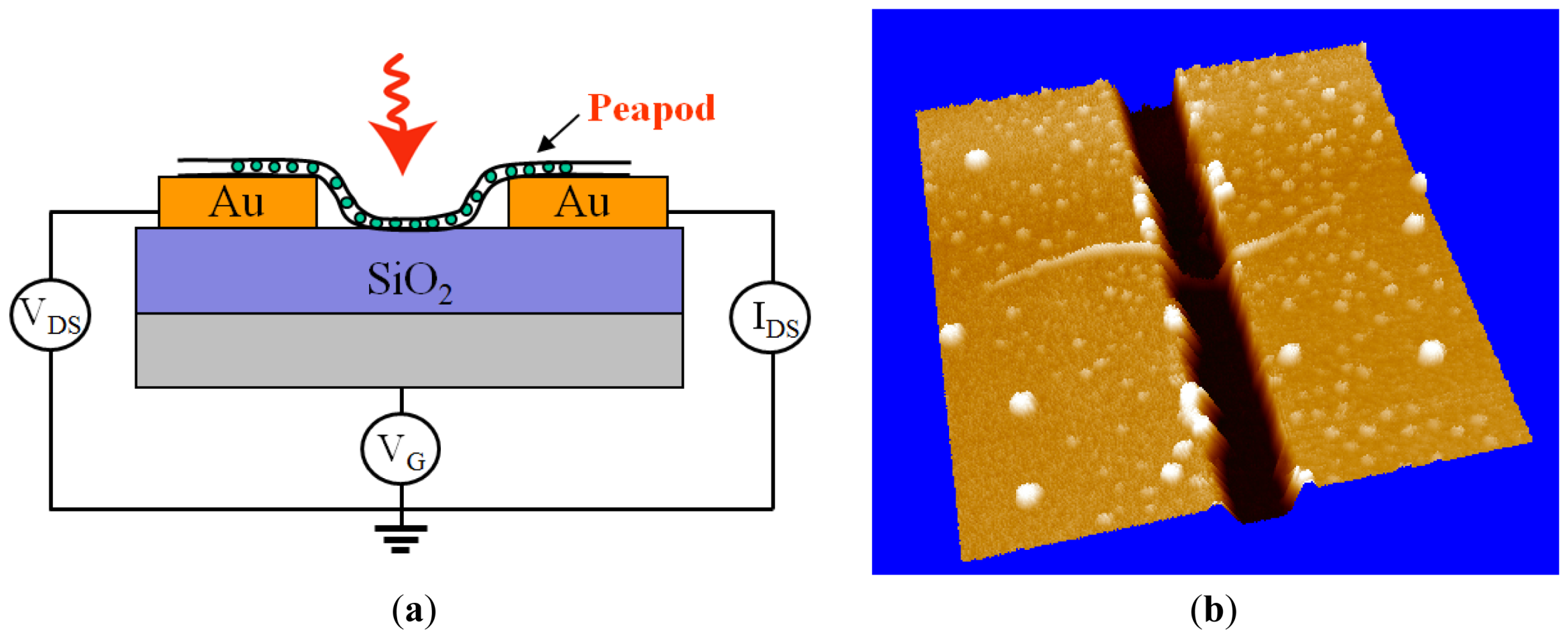
2. Experimental Section
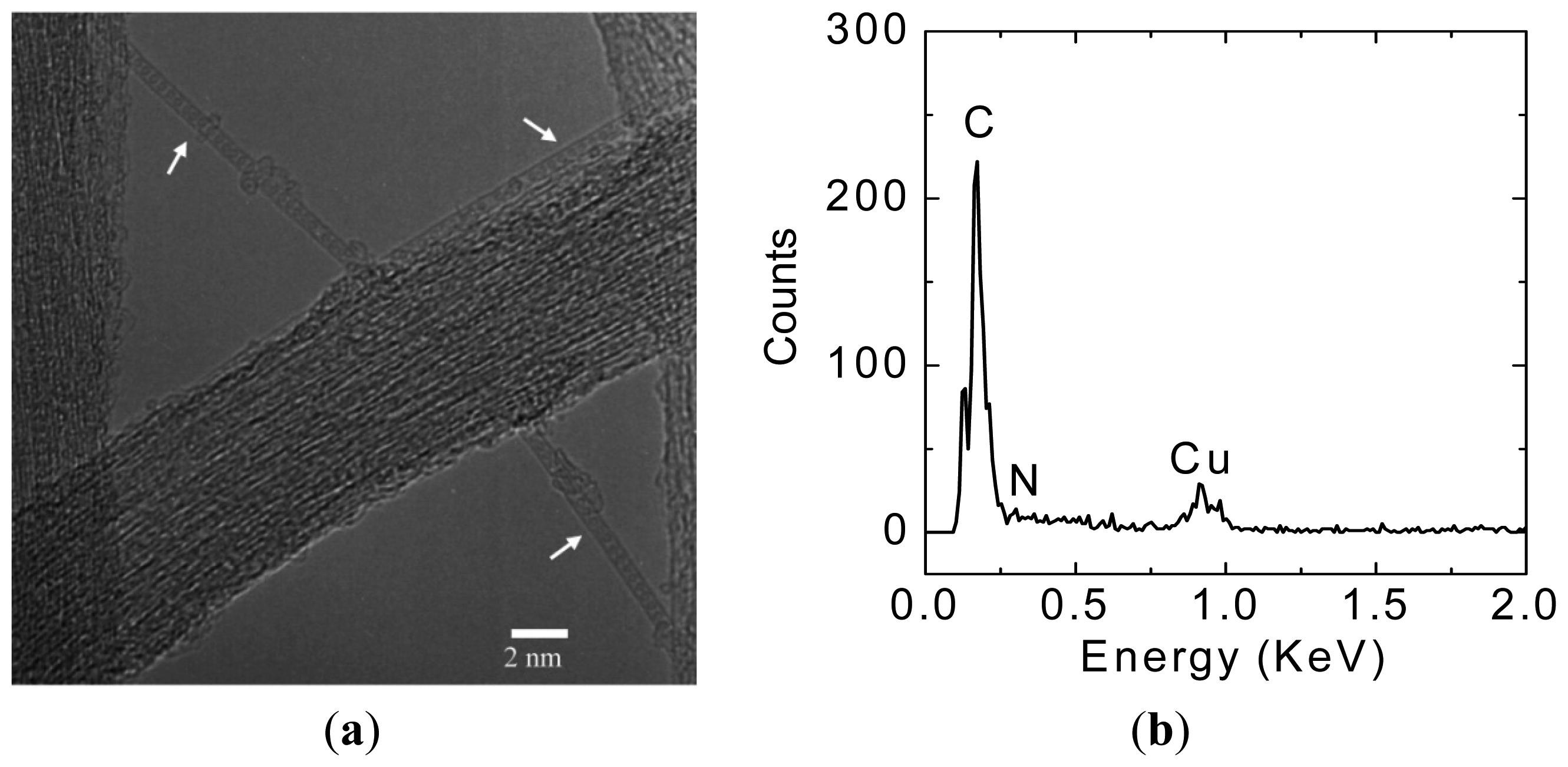
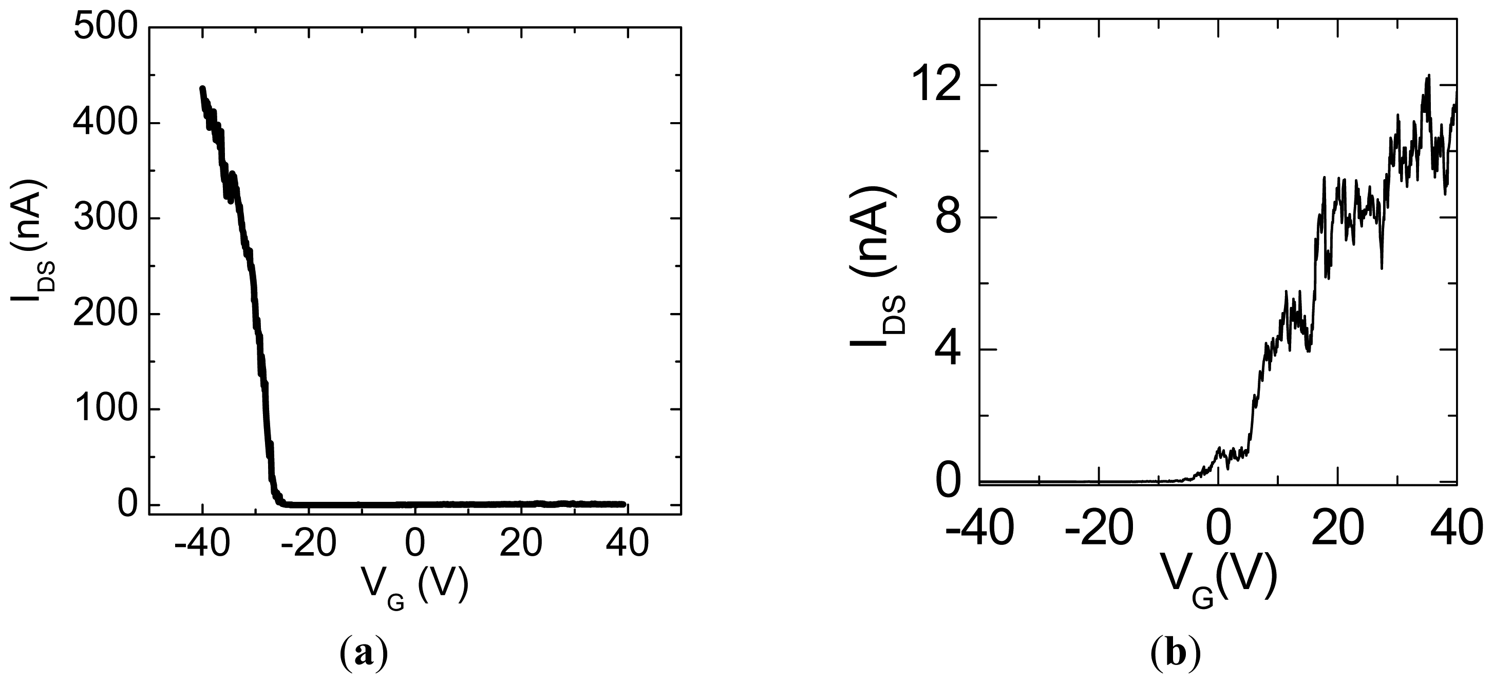
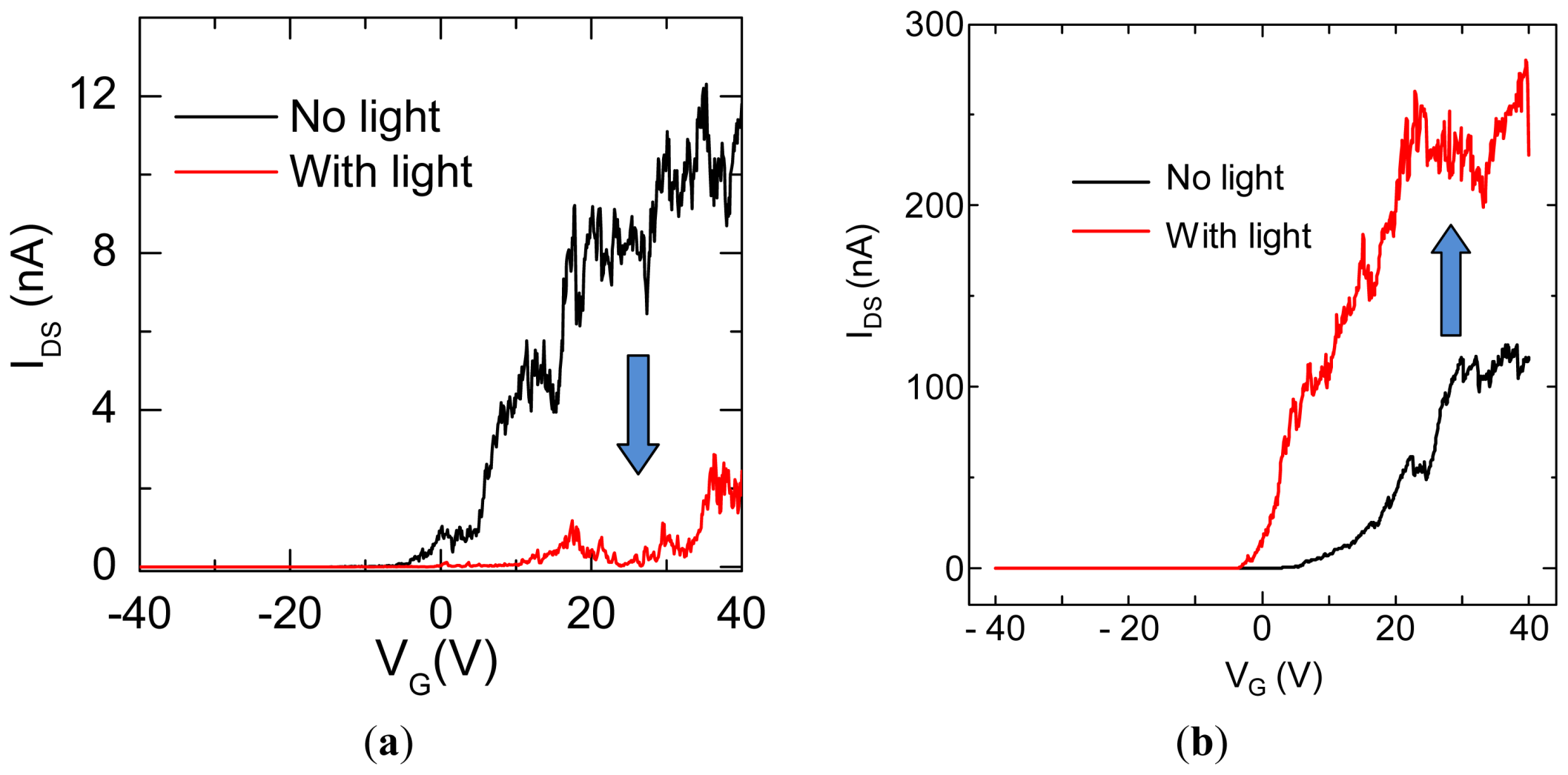
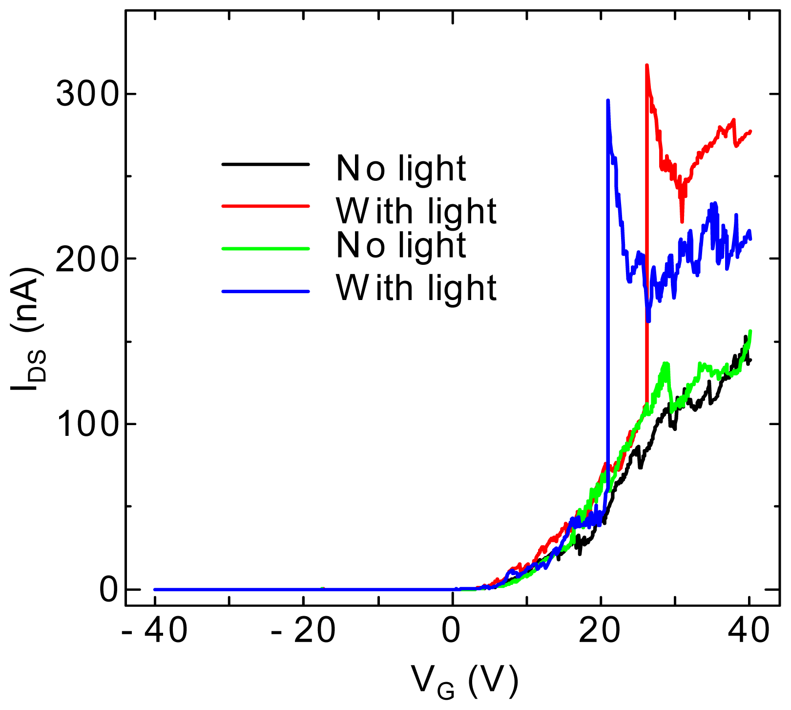
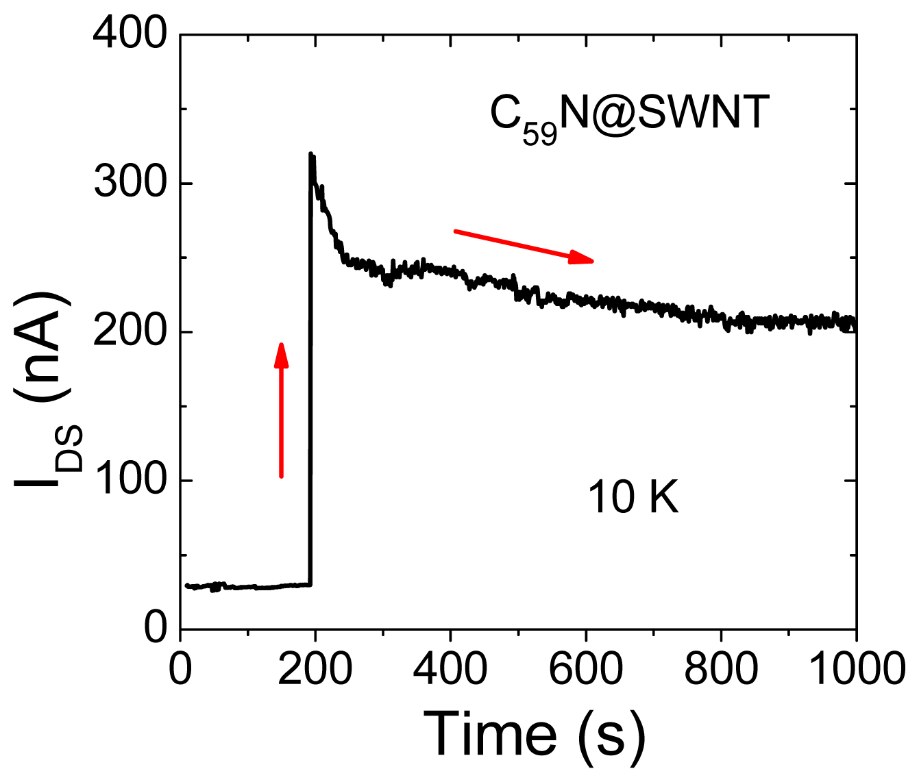
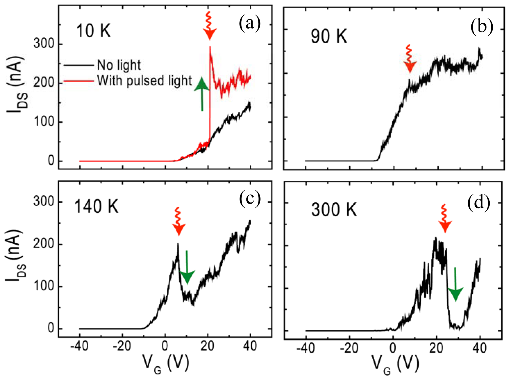
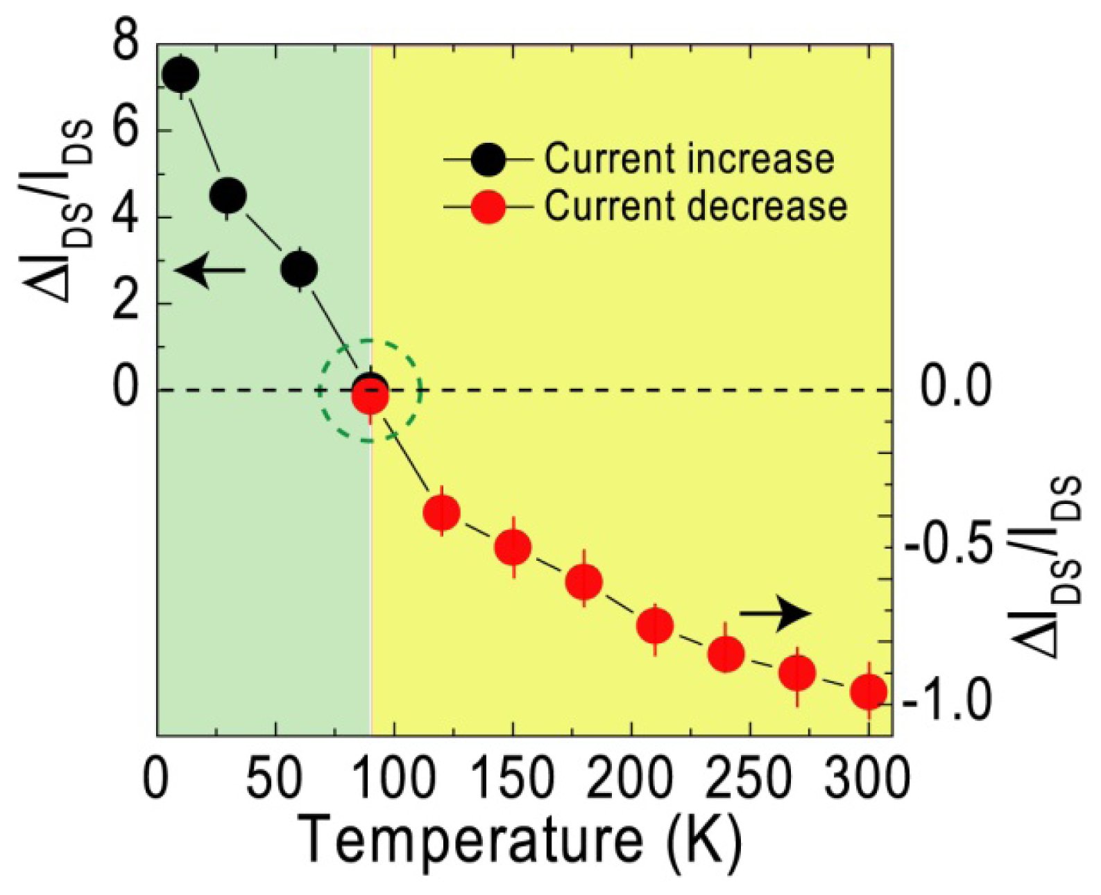
3. Results and Discussion
4. Conclusions
Acknowledgments
References
- Gao, Y.; Bando, Y. Carbon nanothermometer containing gallium. Nature 2002, 415, 599. [Google Scholar]
- Pradhan, B.; Setyowati, K.; Liu, H.; Waldeck, D.H.; Chen, J. Carbon nanotube–polymer nanocomposite infrared sensor. Nano Lett. 2008, 8, 1142–1146. [Google Scholar]
- Ulissi, Z.W.; Zhang, J.; Boghossian, A.A.; Reuel, N.F.; Shimizu, S.F.E.; Braatz, R.D.; Strano, M.S. Applicability of birth–death markov modeling for single-molecule counting using single-walled carbon nanotube fluorescent sensor arrays. J. Phys. Chem. Lett. 2011, 2, 1690–1694. [Google Scholar]
- Kauffman, D.R.; Sorescu, D.C.; Schofield, D.P.; Allen, B.L.; Jordan, K.D.; Star, A. Understanding the sensor response of metal-decorated carbon nanotubes. Nano Lett. 2010, 10, 958–963. [Google Scholar]
- Wang, L.; Chen, W.; Xu, D.; Shim, B.S.; Zhu, Y.; Sun, F.; Liu, L.; Peng, C.; Jin, Z.; Xu, C.; Kotov, N.A. Simple, rapid, sensitive, and versatile SWNT–paper sensor for environmental toxin detection competitive with ELISA. Nano Lett. 2009, 9, 4147–4152. [Google Scholar]
- Fu, Q.; Lu, C.; Liu, J. Selective coating of single wall carbon nanotubes with thin SiO2 layer. Nano Lett. 2002, 2, 329–332. [Google Scholar]
- Mubeen, S.; Zhang, T.; Chartuprayoon, N.; Mulchandani, A.Y.R.; Myung, N.V.; Deshusses, M.A. Sensitive detection of H2S using gold nanoparticle decorated single-walled carbon nanotubes. Anal. Chem. 2010, 82, 250–257. [Google Scholar]
- An, K.H.; Jeong, S.Y.; Hwang, H.R.; Lee, Y.H. Enhanced sensitivity of a gas sensor incorporationg single-walled carbon nanotub-polypyrrole nanocomposites. Adv. Mater. 2004, 16, 1005–1009. [Google Scholar]
- Star, A.; Joshi, V.; Skarupo, S.; Thomas, D.; Gabriel, J.-C.P. Gas sensor array based on metal-decorated carbon nanotubes. J. Phys. Chem. B 2006, 110, 21014–21020. [Google Scholar]
- Shirsat, M.D.; Sarkar, T.; Kakoullis, J.; Myung, N.V., Jr.; Konnanath, B.; Spanias, A.; Mulchandani, A. Porphyrin-functionalized single-walled carbon nanotube chemiresistive sensor arrays for VOCs. J. Phys. Chem. C 2012, 116, 3845–3850. [Google Scholar]
- Kaneko, T.; Li, Y.F.; Nishigaki, S.; Hatakeyama, R. Azafullerene encapsulated single-walled carbon nanotubes with n-type electrical transport property. J. Am. Chem. Soc. 2008, 130, 2714–2715. [Google Scholar]
- Li, Y.F.; Kaneko, T.; Kong, J.; Hatakeyama, R. Photoswitching in azafullerene encapsulated single-walled carbon nanotube FET devices. J. Am. Chem. Soc. 2009, 131, 3412–3413. [Google Scholar]
- Cuong, N.T.; Otani, M.; Iizumi, Y.; Okazaki, T.; Rotas, G.; Tagmatarchis, N.; Li, Y.F.; Kaneko, T.; Hatakeyama, R.; Okada, S. Orgin of n-type transport behavior of azafullerene encapsualted single-walled carbon nanotubes. Appl. Phys. Lett. 2011, 99. [Google Scholar]
- Li, Y.F.; Kaneko, T.; Miyanaga, S.; Hatakeyama, R. Synthesis and property characterization of C69N azafullerne encapsulated single-walled carbon nanotubes. ACS Nano 2010, 4, 3522–3526. [Google Scholar]
- Andreoni, W.; Curioni, A.; Holczer, K.; Prassides, K.; Keshavarz-K, M.; Hummelen, J.; Wudl, F. Unconventional bonding of azafullerenes: Theory and experiment. J. Am. Chem. Soc. 1996, 118, 11335–11336. [Google Scholar]
- Xie, R.; Bryant, G.W.; Sun, G.; Nicklaus, M.C.; Heringer, D.; Frauenheim, Th.; Manaa, M.R.; Smith, V.H., Jr.; Araki, Y.; Ito, O. Excitations, optical absorption spectra, and optical excitonic gaps of heterofullerenes. I. C60, C59N+, and C48N12: Theory and experiment. J. Phys. Chem. 2004, 120, 5133–5147. [Google Scholar]


© 2013 by the authors; licensee MDPI, Basel, Switzerland. This article is an open access article distributed under the terms and conditions of the Creative Commons Attribution license (http://creativecommons.org/licenses/by/3.0/).
Share and Cite
Li, Y.; Kaneko, T.; Hatakeyama, R. C59N Peapods Sensing the Temperature. Sensors 2013, 13, 966-974. https://doi.org/10.3390/s130100966
Li Y, Kaneko T, Hatakeyama R. C59N Peapods Sensing the Temperature. Sensors. 2013; 13(1):966-974. https://doi.org/10.3390/s130100966
Chicago/Turabian StyleLi, Yongfeng, Toshiro Kaneko, and Rikizo Hatakeyama. 2013. "C59N Peapods Sensing the Temperature" Sensors 13, no. 1: 966-974. https://doi.org/10.3390/s130100966
APA StyleLi, Y., Kaneko, T., & Hatakeyama, R. (2013). C59N Peapods Sensing the Temperature. Sensors, 13(1), 966-974. https://doi.org/10.3390/s130100966