Toward 100 Mega-Frames per Second: Design of an Ultimate Ultra-High-Speed Image Sensor

Abstract
:
1. Introduction
1.1. Evolution of the CCD-ISIS
- Parallel/Partial Readout Imaging Scheme (PPR):This is the most common technique to increase the frame rate simply by reading out image signals in parallel through many readout taps, and/or partially only from a selected area in the imaging area.
- In situ Storage Imaging Scheme (ISIS):A number of storage elements are placed within or nearby each pixel to store a number of consecutively captured images. The ISIS camera operates at an ultra-high frame rate with a frame interval equal to the time required for signal electrons generated in photo-diodes move to the nearby storage elements [1–6].
- A BSI-ISIS with the maximum frame rate achievable by a current standard CCD technology.
- A BSI-ISIS with the theoretical maximum frame rate.
1.2. The Design Experience of ISIS-100M
2. General Description of the ISIS-100M
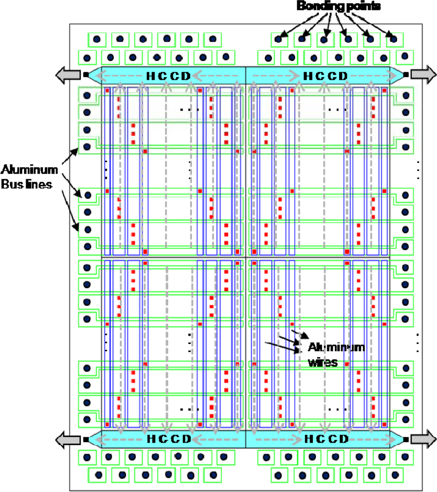
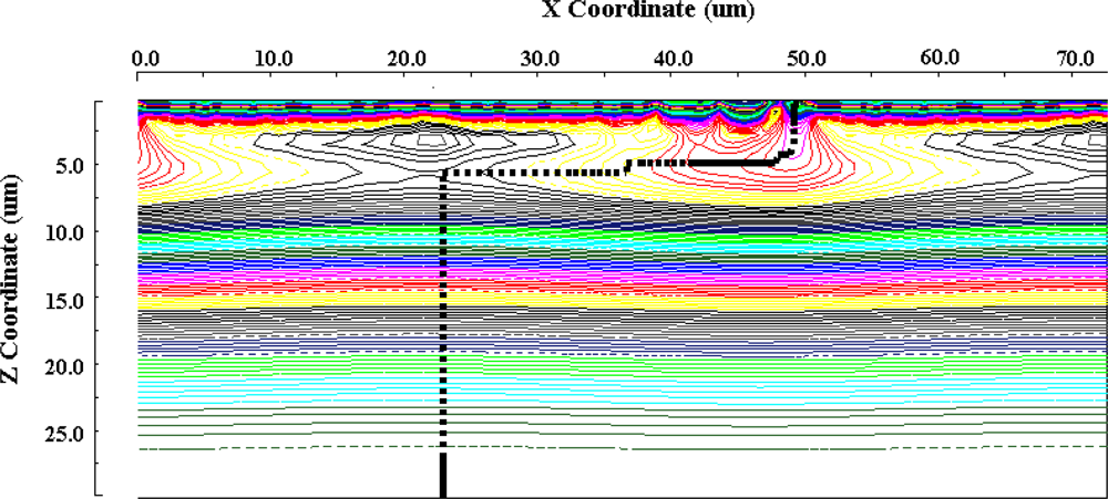
2.1. Plane and Cross Section Structure
2.2. Basic Performance
3. Technologies to Achieve Ultra-high Frame Rate
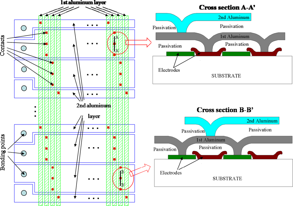
- Two-phase-transfer CCD: Although the two-phase transfer is a common CCD technology, it increases the frame rate when combined with differential driving voltage transfer. However, employment of the two-phase transfer functions to increase the frame rate by the combination with the complementary internal bus lines explained later. The contact structures between the polysilicon and metal layers are simplified, which makes it easy to employ multi-metal layers to reduce parasitic impedance in transfer of the driving voltages.
- The wafer with double-epi layers: To form the cross-section structure shown in Figures 2 (b) and (c), a dedicated wafer with n- and p-double epi-layers with gradated concentration profiles is used as the starting material [16].
- Three-layer p-well design: An innovative design with three p-well layers is introduced to generate a smoothly changing potential gradient toward the collection gate and to protect the storage CCD channels from migration of generated photoelectrons. The p-well of each pixel has two holes: a large one at the collection gate is to introduce photoelectrons to the storage CCD channels on the front side; a small one at the drain to collect five percent of the generated photo-electrons to monitor in real time a sudden change in the average brightness, which serves as an index for occurrence of a target event.
- Curved CCD design: Since the very early development stage of the CCD-ISIS group, a curved design has been introduced to transfer photoelectrons smoothly and swiftly [17].
- Microlens array: In design of common imagers, microlens arrays are mainly used to increase the nominal fill factor. For BSI-ISIS, they contribute to pixel separation for oblique incident light to increase the frame rate.
- Wiring layout to minimize RC delay in driving voltage transfer: Attenuation of driving voltages of the ISIS-V12 is rather high, which limited the maximum frame rate for the full well capacity at 250,000 fps. We developed a simple yet accurate evaluation method to estimate the attenuation of the sensor without time-consuming full-scale circuit simulation [18].
- Complementary global bus-lines: An innovative, CCD-specific design is introduced to reduce the inductance of the two-phase bus lines. This is required to allow the high frequency current flows needed to drive the ISIS-100M at 100 Mfps.
4. Acceleration of Photo-Electrons Transport from the Backside to Collection Gate
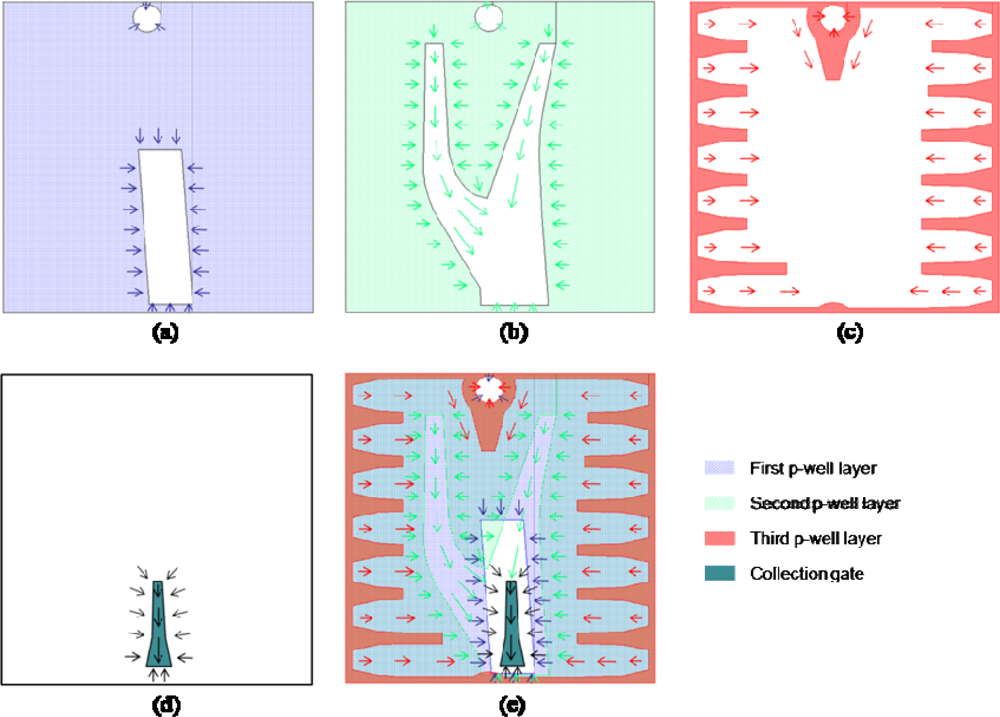
4.1. Special P-well Layer Design
- To confine photo-electrons generated in the generation layer at the backside within the pixel area.
- To make a p-well protect the storage area from migration of signal electrons.
- To accelerate their horizontal transfer speed.
- To smoothly introduce them to the collection gate and to the input gate under the p-well.
- The first layer covers most of the pixel area except the collection gate, which creates a horizontal barrier.
- The second layer also covers most of the pixel area and also serves as a horizontal barrier. Besides, there are two trunk-like large holes stretching toward the top left and top right corner of the pixel, respectively. The holes were designed to have a widening exponential shape toward the collection gate to generate a potential gradient vertically downward the collection gate. The bifurcation of this layer design is introduced to separate the electron path to the collection gate from the path to the drain through the small hole for a video trigger.
- The last p-well layer consists of a finger-like structure around the pixel perimeter to define pixel boundaries. It also has one trapezoid stretching downward from the small hole to separate the electron paths.
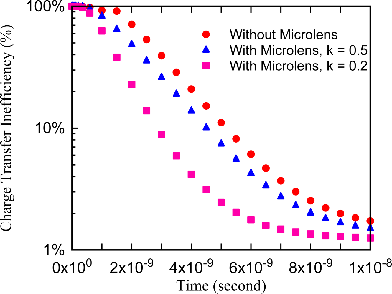
4.2. Electron Transit Time and Efficiency of Micro-Lens Array
- Ten thousands photoelectrons are generated at once at and distributed uniformly over the back surface of each pixel.
- A microlens on the pixel collects and uniformly distributes the electrons in the central area of the back surface: the area is 50% or 20% of the back surface as depicted in Figure 7.
- Without the microlens, 90% of electrons are transferred within 5 ns.
- The microlens with a light collection rate of 50% is not so effective. However, if the collection rate is 20%, the efficiency is significantly improved and 97.2% of electrons reach the collection gate within 5 ns.
- It is impossible to achieve transfer of 100% of electrons for 100 Mfps.
- More than 90% can be transferred.
- If we employ a microlens array and an appropriate post-processing technology, the frame rate very close to 100 Mfps can be achieved.
5. Technology to Deliver Driving Voltages
5.1. Metal Layout to Reduce RC Delay in Driving Voltage Transfer
- An additional aluminum layer used as bus lines placed on the imaging area.
- Direct bonding of wires from external circuitry to each bus line.
5.2. Application of Differential Bus Lines
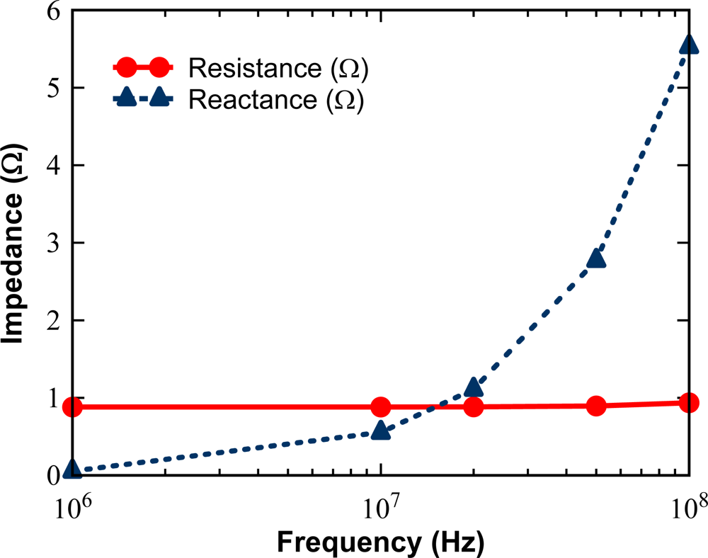
- In order to reduce RC delay, the global bus lines have to be wide and thick enough to reduce their resistances. This makes reactance part comparable or even greater than resistance part in the parasitic impedance.
- As the frequency increases, driving voltage waveform contains higher frequency components, which makes the inductance effect more significant.
- Skin effect appears on resistance for frequencies larger than 20 MHz. However, up to 100 MHz, the effect can be neglected in practical designs.
- Effect of magnetic inductance is very large. The condition ωL = 0.1R is obtained at a frame rate of 2 Mfps, much slower than our design target of 100 Mfps.
5.3. Crossed Bundling
6. CCD-CMOS Hybrid Ultra-High-Speed Image Sensor: RA-ISIS
- With a gap narrower than 0.2 μm between adjacent transfer gate electrodes, a smoothly changing potential profile is created in the buried CCD channel. Recent deep-submicron CMOS processes allow fabrication of polysilicon gates with the gap less than 0.2 μm.
- Only minor process modification is required. To increase full well capacity and create a smooth channel potential beneath the poly-poly gap, thickening of the oxide insulation layer is necessary.
- Various other CCD related technologies had been introduced to the advanced CMOS image sensor process such as deep implanting, floating diffusion amplifier, correlated double sampling technique, etc.
- Advanced CMOS processes utilize four or more metal layers, from which two upper metal layers are allocated to the crossed differential internal bus lines to significantly reduce the inductance.
- The very fine design rule makes possible scaling of the CCD-ISIS, which is the simplest way to increase the maximum frame rate. For example, when the driving voltage transfer is the limiting factor on the maximum frame rate, by reducing the width of the chip to a half of the original size, resistance and inductance of the internal bus lines and the capacitance of the buried CCD channels all reduces to the halves of the original values. As a result, the total power load for the driving voltage transfer is reduced to a quarter, which increases the maximum frame rate four times.
- Incorporating CMOS readout technology with CCD in situ storage, we can obtain an ultimate high speed image sensor with flexible and high speed readout by CMOS technology and ultra-high-speed and superior image quality by CCD technology.
7. Other Technical Problems
- Heat generation
- Removal of positive charge carriers (holes) from the backside
- Compact high-power driver IC
- Integrated packaging
8. Conclusions
- The time required for photo-electrons generated at the backside to reach the storage CCD on the front side is minimized by employment of the wafers with double-epi layers, the special three-layer p-well design, the curved CCD design and a microlens array.
- The RC-delay is minimized by introducing one additional layer for the internal bus lines and directly bonding them to wires from external circuitry. A simple estimation method developed by the authors contributes to optimization of the metal wiring.
- Inductance of the internal bus lines is minimized by the proposed crossed differential bus lines, which is specifically efficient to drive CCDs.
- The chip size is minimized to fabricate the CCD-ISIS using an advanced sub-micron CMOS image sensor process.
References and Notes
- Kosonocky, W.K.; Yang, G.; Ye, C.; Kabra, R.; Lawrence, J.; Mastrocolla, V.; Long, D.; Shallcross, F.; Patel, V. 360 × 360-Element Very High Burst-Frame Rate Image Sensor. IEEE International Solid-State Circuits Conference (ISSCC), Digest of Technical Papers, San Francisco, CA, USA, February 6–8, 1996; pp. 182–183.
- Etoh, T.G.; Poggerman, D.; Ruckelshausen, A.; Theuwissen, A.J.P.; Kreider, G.; Folkerts, H.O.; Mutoh, H.; Kondo, Y.; Maruno, H.; Takubo, K.; Soya, H.; Takehara, K.; Okinaka, T.; Takano, Y.; Reisinger, T.; Author; Lohman, C.B. A CCD Image Sensor of 1M frames/s for Continuous Image Capturing of 103 Frames. IEEE International Solid-State Circuits Conference (ISSCC), Digest of Technical Papers, San Francisco, CA, USA, February 4–6, 2002; pp. 46–47.
- Etoh, T.G.; Poggerman, D.; Kreider, G.; Mutoh, H.; Theuwissen, A.J.P.; Ruckelshausen, A.; Kondo, Y.; Maruno, H.; Takubo, K.; Soya, H.; Takehara, K.; Okinaka, T.; Takano, Y. An Image Sensor Which Captures 100 Consecutive Frames at 1,000,000 frame/s. IEEE Trans. Electron Devices 2003, 50, 144–151. [Google Scholar]
- Ohtake, H.; Hayashida, T.; Kitamura, k.; Arai, T.; Yonai, J.; Tanioka, K.; Maruyama, H.; Etoh, T.G. 300,000-Pixel Ultra-High-Speed High-Sensitivity CCD and a Single-Chip Color Video Camera Mounting This CCD. Broadcast Technol. NHK STRL 2006, 28, 2–9. [Google Scholar]
- Vo Le, C.; Etoh, T.G.; Nguyen, H.D.; Dao, V.T.S.; Soya, H.; Lesser, M.; Oullette, D.; van Kujik, H.; Bosiers, J.; Ingram, G. A Backside-Illuminated Image Sensor with 200,000 Pixels Operating at 250,000 Frames per Second. IEEE Trans. Electron Devices 2009, 56, 2556–2562. [Google Scholar]
- Lazovsky, L.; Cismas, D.; Allan, G.; Given, D. CCD Sensor and Camera for 100 Mfps Burst Frame Rate Image Capture. Proceedings of Airborne Intelligence, Surveillance, Reconnaissance (ISR) Systems and Applications II, Orlando, FL, USA, March 28–April 1, 2005; pp. 184–190.
- Photron Corporation, FASTCAM SA-5 Product Specification. Available online: http://www.photron.com/index.php?cmd=product_general&product_id=7 (accessed on 19 December 2009).
- El-Desouki, M.; Deen, M.J.; Fang, Q.; Liu, L.; Tse, F.; Armstrong, D. CMOS Image Sensors for High Speed Applications. Sensors 2009, 9, 430–444. [Google Scholar]
- Thoroddsen, S.T.; Etoh, T.G.; Takehara, K. High-Speed Imaging of Drops and Bubbles. Annu. Rev. Fluid Mech 2008, 40, 257–285. [Google Scholar]
- Shiraga, H.; Heya, M.; Azechi, H.; Yamanaka, T.; Mima, K. One-and Two-Dimensional Fast x-ray Imaging of Laser-Driven Implosion Dynamics with x-ray Streak Camera. Rev. Sci. Instrum 1998, 68, 828–830. [Google Scholar]
- Kubota, T.; Komai, K.; Yamagiwa, M.; Awatsuji, Y. Moving Picture Recording and Observation of Three-Dimensional Image of Femtosecond Light Pulse Propagation. Opt. Express 2007, 15, 14348–14354. [Google Scholar]
- Goda, K.; Tsia, K.K.; Jalali, B. Serial Time-Encoded Amplified Imaging for Real-Time Observation of Fast Dynamic Phenomena. Nature 2009, 458, 1145–1149. [Google Scholar]
- Etoh, T.G.; Vo Le, C.; Kawano, H.; Ishikawa, I.; Miyawaki, A.; Dao, V.T.S.; Nguyen, H.D.; Yokoi, S.; Yoshida, S.; Nakano, H.; Takehara, K.; Saito, Y. Ultra-High-Speed Bionanoscope for Cell and Microbe Imaging. Proceedings of 28th International Congress on High Speed Imaging and Photonics (ICHSIP28), Canberra, Australia, November 9–14, 2008; pp. 712605:1–712605:11.
- Hynecek, J. CCM-A New Low-Noise Charge Carrier Multiplier Suitable for Detection of Charge in Small Pixel CCD Image Sensors. IEEE Trans. Electron Devices 1992, 39, 1972–1975. [Google Scholar]
- Fife, K.; El Gamal, A.; Wong, H.S. A 3MPixel Multi-Aperture Image Sensor with 0.7c μm Pixels in 0.11 μm CMOS. IEEE International Solid-State Circuits Conference (ISSCC), Digest of Technical Papers, San Francisco, CA, USA, February 3–7, 2008; pp. 48–49.
- Etoh, T.G.; Hayashida, T.; Maruyama, H.; Arai, T.; Uchiyama, N.; Sakamoto, T. Backside Illuminated Image Sensors Manufactured with Gradatetd Double Epitaxial Layers: an Application to a High-Speed Hish-Sensitivity Image Sensor. Proceedings of the International Image Sensor Workshop (IISW), Bergen, Norway, June 26–28, 2009. in press.
- Poggemann, D. Simulation-Based Design of a CCD Image Sensor for 1 Million Frames per Second, 1st ed.; Der Andere Verlag: Tonning, Germany, 2005; pp. 92–103. [Google Scholar]
- Dao, V.T.S.; Etoh, T.G.; Vo Le, C.; Nguyen, H.D.; Takehara, K.; Akino, T.; Nishi, K. Estimation of Driving Voltage Attenuation of An Ultra-High-Speed Image Sensor by Dimensional Analysis. World Acad. Sci. Eng. Technol. Int. J. Electron. Circ. Syst 2008, 2, 200–204. [Google Scholar]
- Kamon, M.; Tsuk, M.J.; White, J. Fasthenry: a Multipole-Accelerated 3-D Inductance Extraction Program. IEEE Trans. Microwave Theory 1994, 42, 1750–1758. [Google Scholar]
- Ito, H.; Gomi, S.; Sugita, H.; Okada, K.; Masu, K. Twisted Differential Transmission Line Structure for Global Interconnect in Si LSI. Jpn. J. Appl. Phys 2005, 44, 2774–2779. [Google Scholar]
- Worm, S.; Banda, Y.; Bowdery, C.; Buttar, C.; Clarke, P.; Cussans, D; Damerell, C.; Davies, G.; Devetak, E.; Fopma, J.; Foster, B.; Gao, R.; Gillman, A.R.; Goldstein, J.; Greenshaw, T; Grimes, M.; Harder, K.; Hawes, B.; Heath, H.; Hillert, S.; Jeffery, B.; Johnson, E.; Kundu, N.; Martin, V.; Murray, P.; Nichols, A.; Nomerotski, A.; O’Shea, V.; Parkes, C.; Perry, C.; Woolliscroft, T.; Sopczak, A; Stefanov, K.; Thomas, S.; Tikkanen, T.; Yang, S.; Zhang, Z. Progress with Vertex Detector Sensors for the International Linear Collider. Proceedings of 15th International Workshop on Vertex Detectors (VERTEX), Perugia, Italy, September 25–29, 2006; pp. 839–842.
- Hawes, B.; Cussans, D.; Damerell, C.; Devetak, E.; Fopma, J.; Gao, R.; Goldstein, J.; Greenshaw, T.; Hillert, S.; Kundu, N.; Nomerotski, A.; Perry, C.; Stefanov, K.; Thomas, S.; Worm, S. Planar Transformers for Column Parallel CCD Clock Drive. Nucl. Instrum. Meth. A 2009, 609, 122–128. [Google Scholar]


| Sensor/Camera | Frontside illuminated | Backside illuminated | ||
|---|---|---|---|---|
| ISIS-V2 [2,3] | ISIS-V4 [4]+ | ISIS-V12 [5,13] | ISIS-100M* | |
| Pixel count (pixels) | 81,120 (312 × 260) | 302,400 (420 × 720) | 201,600 (480 × 420) | 140,800 (440 × 320) |
| Maximum frame rate | 1 Mfps | 1 Mfps | 1 Mfps | 100 Mfps |
| Technologies for high sensitivity | N/A | N/A | CCM/Backside illumination/Cooling | Backside illumination/Cooling |
| Frame Rate | 30–100,000,000 fps |
| Pixel Count | 440 × 320 (=140,800) pixels |
| Pixel Size | 50.4 × 50.4 μm2 |
| CCD element size | 3.6 × 3.6 μm2 |
| Number of Stored Images | 126 frames |
| Full well Capacity | 8,000 electrons |
| Grey Level | >9 bits |
| Overwriting Drain | Installed |
| On-chip trigger system | Installed |
| Transfer Scheme | 2-phase transfer for VCCD, voltage swing 10 V 4-phase transfer for HCCD, voltage swing 5 V |
| Cases |  (a) |  (b) |  (c) |
| Magnetic energy (ME) profile |  |  |  |
| Relative ME | 100% | 25% | 0.5% |
| ωL/R | 600% | 150% | 3% |
©2010 by the authors; licensee Molecular Diversity Preservation International, Basel, Switzerland. This article is an open access article distributed under the terms and conditions of the Creative Commons Attribution license (http://creativecommons.org/licenses/by/3.0/)
Share and Cite
Vu Truong Son, D.; Goji Etoh, T.; Tanaka, M.; Hoang Dung, N.; Le Cuong, V.; Takehara, K.; Akino, T.; Nishi, K.; Aoki, H.; Nakai, J. Toward 100 Mega-Frames per Second: Design of an Ultimate Ultra-High-Speed Image Sensor. Sensors 2010, 10, 16-35. https://doi.org/10.3390/s100100016
Vu Truong Son D, Goji Etoh T, Tanaka M, Hoang Dung N, Le Cuong V, Takehara K, Akino T, Nishi K, Aoki H, Nakai J. Toward 100 Mega-Frames per Second: Design of an Ultimate Ultra-High-Speed Image Sensor. Sensors. 2010; 10(1):16-35. https://doi.org/10.3390/s100100016
Chicago/Turabian StyleVu Truong Son, Dao, Takeharu Goji Etoh, Masatoshi Tanaka, Nguyen Hoang Dung, Vo Le Cuong, Kohsei Takehara, Toshiro Akino, Kenji Nishi, Hitoshi Aoki, and Junichi Nakai. 2010. "Toward 100 Mega-Frames per Second: Design of an Ultimate Ultra-High-Speed Image Sensor" Sensors 10, no. 1: 16-35. https://doi.org/10.3390/s100100016
APA StyleVu Truong Son, D., Goji Etoh, T., Tanaka, M., Hoang Dung, N., Le Cuong, V., Takehara, K., Akino, T., Nishi, K., Aoki, H., & Nakai, J. (2010). Toward 100 Mega-Frames per Second: Design of an Ultimate Ultra-High-Speed Image Sensor. Sensors, 10(1), 16-35. https://doi.org/10.3390/s100100016