Abstract
Delafossite CuFeO2 has emerged as a promising earth-abundant p-type photocathode for solar fuel generation due to its stability in aqueous conditions and its favorable light absorption characteristics. However, practical photocurrent generation in CuFeO2 has consistently fallen short of its theoretical potential. This limitation is attributed primarily to suboptimal practical visible light absorption, resulting in diminished incident photon-to-current conversion efficiency (IPCE). Challenges related to charge separation and transport, originating from low acceptor density and inherent low conductivity, further contribute to the reported suboptimal performance of delafossite CuFeO2. Thus, the present review comprehensively documents the latest advancements in the field of CuFeO2 photocathode research, with a particular emphasis on strategies to overcome the challenges currently being faced and on the illustration of pathways that may lead to the enhancement of critical performance parameters such as photocurrents, photovoltage, and fill factor.
1. Introduction
Hydrogen, a carbon-free energy carrier, holds immense promise for various energy sectors, including industry and transportation, owing to its relatively high gravimetric energy density (143 MJ kg−1) [1,2,3,4]. The development of a global hydrogen economy is widely regarded as a critical pathway toward achieving energy sustainability and decarbonization, offering solutions to energy security, environmental degradation, and industrial decarbonization. However, technical and economic barriers such as high production costs, inefficient storage/delivery infrastructure, and reliance on fossil fuel-derived hydrogen must be urgently addressed. These challenges are compounded by escalating threats from climate change, including global warming, ocean acidification, and air pollution, which have intensified since the industrial revolution [5]. Hydrogen can be efficiently stored, transported, and utilized as fuel in eco-friendly fuel cells or combustion engines without generating harmful pollutants [6,7,8]. By 2050, an estimated 61,737 TWhLHV of hydrogen will be required to fully defossilize the global energy-industry system, necessitating scalable and sustainable production methods [9]. Diverse methods for hydrogen production exist, including steam methane reforming [10], oil reforming [11], and coal and biomass gasification [12,13], as well as water splitting [14]. Today, approximately 90% of global hydrogen production relies on steam methane reforming and fossil fuel gasification. Nevertheless, the purity of hydrogen from these methods remains unsatisfactory, and its generation is generally accompanied by substantial CO2 emissions [15,16,17]. In contrast, electricity- or light-driven water splitting, an environmentally sustainable approach, has garnered significant attention as a sustainable means of hydrogen production.
Solar water splitting, which utilizes solar energy and abundant water resources, can be accomplished through the utilization of photovoltaic systems coupled with electrolysis (PV-E), photocatalytic (PC), and photoelectrochemical (PEC) water splitting [18]. While PV-E boasts high efficiency, its complexity results in higher production costs [19]. In contrast, PC and PEC systems, in which light-absorbing properties and the electrolyzers’ functionality are combined in a single device, potentially offer a more cost-effective approach. Of these, PEC systems enable separation of the oxygen evolution reaction (OER) and hydrogen evolution reaction (HER) at distinct electrodes, providing a commercially viable path to sustainable hydrogen production as costs continue to decline [20]. PC systems are expected to be the most cost-effective method for hydrogen production, but separating potentially explosive hydrogen–oxygen mixtures remains a major bottleneck. This concern arises because the OER and HER usually occur at the same material without spatial separation, and in the reactor, accumulation of both oxygen and hydrogen is likely to occur.
Various photoelectrochemical cell configurations for water splitting have been reported [21,22,23], with the simplest being composed of a single light-absorbing material. This setup includes a photoanode Figure 1a (or photocathode Figure 1b) made of an n-type (or p-type) semiconductor, along with a metal electrode working in the dark, serving as a cathode (or anode). Upon absorption of photons with sufficiently high energy, electron–hole pairs are generated, which are then separated within the semiconductor. The minority charge carriers initiate redox reactions at the semiconductor–liquid interface, while the majority carriers are directed toward the back contact and transported to the counter electrode, typically a metal, through an external circuit to support the other half-reaction. If a single absorber material (semiconductor) is used, it must absorb light with photon energies exceeding 1.23 eV to be able to split water without any additional applied bias. However, considering the well-known overpotentials of the hydrogen and oxygen evolution reaction, a bandgap of at least 2 eV is needed for efficient photoelectrochemical water splitting [22], limiting the use of the solar spectrum. To address this limitation, a more practical approach known as the tandem cell approach has been proposed (see Figure 1c). In tandem cell configurations, a pair of photo-absorbers, a photocathode, and a photoanode enable utilization of different parts of the solar spectrum and the generation of the required photovoltage for water splitting. Calculations have shown that a single absorber PEC system can achieve a maximum solar-to-hydrogen (STH) efficiency of 19.7%, while with tandem systems with two absorbers, STH values of 22.0% to 24.5% might be achievable [24]. To attain such high efficiencies, the photoelectrodes must meet several key requirements, including suitable band edge positions for water reduction and oxidation reactions and efficient charge transport. Moreover, the photoelectrode should facilitate hydrogen or oxygen evolution at low overpotentials, offer high chemical stability, and be prepared from low-cost reagents, i.e., nontoxic, and environmentally friendly earth-abundant materials, in a scalable synthesis method (possible materials are summarized in Figure 1d) [25,26,27].
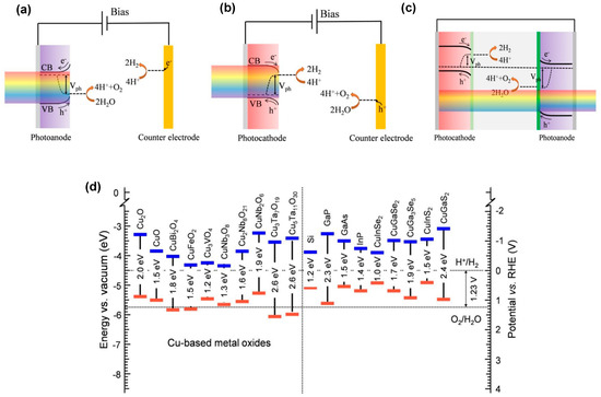
Figure 1.
Principle of operation of PEC cells based on (a) bias-assisted n−type semiconductor, (b) bias-assisted p−type semiconductor, and (c) bias-free tandem structure consisting of p− and n−type photoelectrodes. (d) Energy band diagram of several Cu-based metal oxides together with a wide range of other semiconductors. The dotted lines represent the redox potentials of the relevant water splitting redox couples. Reprinted with permission from ref. [28], Copyright (2020), Energy & Environmental Science.
According to estimates from the U.S. Department of Energy, achieving a solar-to-hydrogen (STH) efficiency of 10% is the fundamental requirement to reach commercial viability of photoelectrochemical (PEC) water splitting [29]. This benchmark efficiency equals to a photocurrent density of 8.2 mAcm−2 using standardized one-sun illumination (AM 1.5 G) [30], as revealed by the correlation of photocurrent density and STH efficiency expressed in Equation (1):
where represents the photocurrent density of the photoelectrode, signifies the Faradaic efficiency of water oxidation or proton reduction at the photoelectrode, and denotes the power of solar irradiation (100 mWcm−2).
The overall efficiency of hydrogen production in PEC cells is predominantly determined by the characteristics of the photoelectrodes involved in the water-splitting processes. This efficiency () can be quantitatively influenced by three factors: (1) the solar light-harvesting efficiency of the photoelectrode (), (2) the charge transport efficiency within the photoelectrode (), and (3) the charge-transfer efficiency at the interface between the photoelectrode and the electrolyte () [31]. In mathematical terms, this relationship can be expressed as follows:
The groundbreaking report on photoelectrochemical (PEC) water splitting, published in 1968, introduced the use of a thin layer of TiO2 with a band gap (Eg) of approximately 3.2 eV as a photoanode in a PEC half-cell. Since then, considerable research efforts have been devoted to the development of photoelectrodes [32]. A range of n-type semiconductors, including n-Si (with an Eg of 1.1–1.3 eV) [33], TiO2 (with an Eg of 3.2–3.4 eV) [34], BiVO4 (with an Eg of 2.2–2.4 eV) [35], WO3 (with an Eg of 2.6–3 eV) [36], g-C3N4 (with an Eg of 2.5–2.8 eV) [37], CdS (with an Eg of 2.2–2.4 eV) [38], SrTiO3 (with an Eg of 3.2–3.4 eV) [39], and Fe2O3 (with an Eg of 2–2.2 eV) [40], have been extensively investigated for their application as photoanodes in PEC cells. Among these materials, TiO2 stands out for its stability, while BiVO4 excels in light absorption in the visible region [41]. It is worth noting that relatively little attention has been paid to the study of photocathodes, despite the extensive research into photoanodes. Efficient photocathodes for PEC water reduction include, among others, semiconductors like Si [42,43], InP [44], CdTe [45], CuInxGa1−xSe2 [46,47], CuInS2 [48], CuGa3Se5 [49], and CuGaSe2 [50,51]. However, the photovoltages generated by these photocathodes fall short of the thermodynamic potential of 1.23 V. The quest for high-photovoltage photocathodes is critical, particularly for constructing highly efficient two-electrode tandem devices alongside high-performance photoanodes, such as BiVO4 or n-Si, to enable bias-free water splitting. In addition, environmental and resource concerns, including the scarcity of indium and gallium and the toxicity of cadmium in CdTe, have driven the search for metal oxide-based photocathodes composed of earth-abundant and non-toxic elements that can be produced by cost-effective and scalable processes [52].
Cu-based binary and ternary metal oxides are promising absorber materials for PEC water reduction when compared to other semiconductor materials like group IV, III-V, and I-III-VI semiconductors. Cu-based oxides exhibit a wide range of bandgap values, ranging from 1.2 to over 3 eV, offering diverse options as efficient light absorbers for solar energy conversion [53]. The majority of Cu-based metal oxides feature conduction band edges situated above the hydrogen evolution potential, rendering the water reduction reaction thermodynamically feasible. Among these, binary oxides such as Cu2O and CuO have band gaps (2.0 and 1.2–1.5 eV) that are suitable for efficient solar light harvesting. However, these photocathodes suffer from photo-corrosion, mainly due to the unfavorable position of the redox couple for Cu2O and CuO reduction situated within the band gap of these semiconductors [54]. A strategic protection approach is therefore essential, with particular focus on interface engineering, band alignment, and carrier transport, all of which are of critical importance in enhancing the PEC performance of binary Cu-based heterojunction photocathodes [55,56].
Copper-based ternary oxides offer a broader spectrum for fine-tuning band structure and optoelectronic properties in comparison with their binary counterparts. Among the ternary oxides, CuBi2O4 has been shown to be a promising photocathode material capable of harnessing visible light and generating substantial photovoltages [57]. With its band gap of approximately 1.8 eV and a reported photocurrent onset potentials of about 1 V vs. the reversible hydrogen electrode (RHE), CuBi2O4 is a material of interest for use in two-electrode tandem photoelectrochemical (PEC) devices [58]. The valence and conduction band edges of CuBi2O4 are composed of Bi 6s and Cu 3d orbitals, respectively [59]. However, in a manner analogous to Cu2O self-reduction, CuBi2O4 photocathodes are susceptible to photocorrosion, presumably as a consequence of the trapping of photoelectrons in the Cu 3d band [60]. Cu-containing delafossites bearing the general formula CuMO2, where M can be Fe, Rh, Cr, Al, Ga, In, or Sc, offer enhanced stability. These materials crystallize in either the rhombohedral (3R) or hexagonal (2H) polytypes, with space groups of Rm (Figure 2a), and P63/mmc (Figure 2b), respectively [61]. In particular, the valence and conduction band edges in Cu-containing delafossites are predominantly composed of Cu 3d and M d or s orbitals. This configuration limits the reduction of Cu(I) by Cu 3d→M d/s electron photoexcitation [62]. Furthermore, the light absorption characteristics of Cu-containing delafossites depend on the cation M and range from ~1.55 eV to band gaps exceeding 3 eV [62].
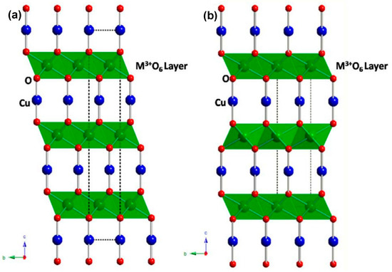
Figure 2.
Two main polymorphic modifications of the delafossite structure that crystallize in the trigonal Rm (a) and hexagonal P63/mmc (b) space groups.
Among these Cu-containing delafossites, CuFeO2, with a small band gap of 1.55 eV, an absorption coefficient of up to α ~ 107 m⁻1, a flat-band potential around 1 V vs. RHE, and its high stability in neutral and basic aqueous environments over extended periods [62], stands out as a promising photocathode material. Its unique combination of earth abundance (Cu and Fe are 50–100× more abundant than In/Ga) [63], non-toxicity, and scalable synthesis routes compared to conventional photocathodes like CdTe or InP makes it a strong candidate for sustainable hydrogen production systems. As summarized in Table 1, CuFeO2 offers notable advantages over state-of-the-art photocathodes in terms of performance, stability, and environmental impact, reinforcing its potential for large-scale hydrogen production. Beyond energy applications, CuFeO2′s stability and electronic properties have also enabled its use in catalytic degradation of pollutants, magnetic devices, and biomedical sensors [64,65,66]. However, despite these promising characteristics that theoretically enable photocurrents of up to 15 mA cm−2, the realized hydrogen evolution efficiencies of CuFeO2 have remain suboptimal [67]. Moreover, measurements utilizing oxygen as an electron scavenger called into question the assumption that CuFeO2 is an efficient PEC water-splitting material [68]. The objective of comprehending and enhancing this unsatisfactory photocurrent density has become a primary focus in CuFeO2 photocathode research. One of the main obstacles to the performance of CuFeO2 photocathodes has been identified as the pinning of the Fermi level at the solid–liquid interface [67,69]. Initially attributed to metal hydroxyl groups on the surface, these states, situated approximately 0.6 eV above the valence band, were later linked to the Fe3+/Fe2+ polaron. Recent studies of CuFeO2 photocathodes have highlighted additional challenges, including limited photogenerated electron diffusion lengths and polaron-mediated charge-carrier recombination [70].

Table 1.
Comparison of photocathode materials for PEC water splitting. Note that the table only provides reference to unprotected photocathodes.
This review focuses on CuFeO2 photocathodes, with a view to elucidating recent endeavors to enhance the material’s performance as a high-efficiency photocathode. We outline the merits and constraints of CuFeO2 as a p-type material, and strategies aimed at addressing challenges associated with the limited PEC performance are categorized. Key techniques that have been successfully applied to the development of CuFeO2-based solar cells and photocathodes will be discussed, thereby highlighting remaining bottlenecks. Additionally, we examine efforts to overcome these limitations and advance CuFeO2 toward practical implementation in photoelectrochemical solar fuel production.
2. Drawbacks of Bare CuFeO2 Photocathodes
Delafossite-phase CuFeO2 has garnered attention as a promising candidate for use as a photocathode, attributed to its intrinsic stability, high absorption coefficient, and a flat band potential of approximately 1 VRHE [71,76,77]. Notably, the hybridization of Cu 3d with O 2p contributes to the valence band (VB), while the conduction band (CB) is composed of Cu 3d and Fe 3d states, leading to a narrow bandgap of around 1.5 eV [78]. The CB edge is situated just above the redox potential of the H+/H2 couple, resulting in favorable electron transfer conditions for hydrogen evolution [71]. Additionally, CuFeO2 exhibits a multi-band absorption spectrum, covering both ultraviolet (UV) and infrared (IR) regions. Despite the theoretically anticipated photocurrents of up to 15 mA cm−2 [77], the actual measured hydrogen evolution efficiencies for bare CuFeO2 have fallen considerably short of these expectations. Table 2 provides an overview of the reported performance of CuFeO2 photocathodes for solar hydrogen production, illustrating the discrepancy between theoretical predictions and experimental results.
Table 2.
Comparison of the PEC water reduction performances of reported CuFeO2-based photocathodes.
CuFeO2-based photocathodes exhibit limited visible light harvesting, often resulting in low incident photon to current conversion efficiencies (IPCE) of >5% in the 600–800 nm wavelength range [3]. The relatively weak absorption and poor charge carrier transport near the absorption edge of this p-type oxide contributes to the poor IPCE [77]. In addition, it has been shown experimentally that the performance of CuFeO2 photocathodes is limited by poor charge separation and slow transport due to low acceptor density, resulting in a low conductivity [80,88].
Fermi-level pinning in iron-containing oxides like hematite (α-Fe2O3) and BiFeO3, linked to redox transition of Fe3+ to Fe2+, has been reported [89,90]. Similar Fermi-level pinning has been observed in CuFeO2 and was attributed to the presence of surface or bulk defect states [67,69]. Distinguishing between bulk and surface defects is crucial as their elimination requires different treatment strategies. While a high density of intrinsic bulk defects can affect a material’s suitability as a photoelectrode, surface defects are more suitable for post-processing strategies and surface modifications, such as the application of overlayers [91] or etching and regrowth strategies [92]. Thus, ongoing efforts aim at discerning whether CuFeO2′s performance stems from bulk or surface defects.
Prévot et al. [71] conducted an intriguing investigation into the performance of a thin film delafossite photocathode using front-side illumination. Their findings unveiled the presence of a smaller electronic band gap, corresponding to an optically forbidden excitation. Water splitting resulted in steady-state photocurrents of approximately 25 μA cm−2 at +0.4 V vs. RHE under chopped light illumination in an argon-purged electrolyte. However, in the presence of a sacrificial electron acceptor, such as oxygen, a dramatic increase in steady-state photocurrents to 1.05 mA cm−2 was observed (Figure 3a). Electrochemical impedance spectroscopy (EIS) revealed that the inversion layer of the p-type electrode was only 0.45 V cathodic to the flat band potential. It was suggested that there may be a smaller electronic band gap associated with an optically forbidden excitation. In their attempt to provide a rational explanation for their observations, Prévot et al. [71] highlighted the lower photocurrents for hydrogen evolution relative to O2 reduction alongside a less-than-unity Faradaic efficiency and suggested that oxygen reduction occurs from mid-gap electronic states. Crucially, the presence of mid-gap electronic states, detected by electrochemical impedance spectroscopy (EIS) (see Figure 3b), cast doubt on the ability of photogenerated carriers to effectively participate in water reduction under illumination. The rate of photogenerated electrons decaying into these low energy states must not exceed their injection into the electrolyte; otherwise, the potential of this material for water reduction would be impeded.
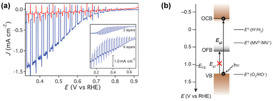
Figure 3.
(a) Linear sweep voltammogram of a six−layer CuFeO2 electrode under intermittent one sun illumination in 1 M NaOH argon-purged electrolyte (red) and oxygen-saturated electrolyte (blue). Inset: wider potential range scans for two- and six-layer electrodes in oxygen-saturated electrolyte. (b) Band energy diagram of CuFeO2 under flat-band conditions. Reprinted with permission from ref. [71], Copyright (2015), ChemSusChem.
Further characterization of the semiconductor-liquid junction (SCLJ) of CuFeO2 using different redox couples in aqueous electrolytes of different pH and in non-aqueous electrolytes (see Figure 4a,b) confirmed a Nernstian behavior of the electronic bands of CuFeO2 over a narrow potential range of 0.77–0.90 V vs. RHE only. This consistent behavior across different redox species suggested the presence of Fermi-level pinning (FLP) located roughly 0.35 V negative to the flat band potential (EFB), as inferred from the photoelectrochemical measurements. Time-resolved microwave conductivity (TRMC) measurements suggested that the bulk material has favorable transport properties, with a long lifetime for photogenerated carriers (about 200 ns) and an associated diffusion length of about 300 nm, suggesting that a photovoltage of 0.8 V can be achieved. Thus, the initially reported band diagram of CuFeO2 was refined by EIS (Figure 4c), Mott–Schottky (MS) analysis (Figure 4d) and Kelvin Probe Force Microscopy (KPFM) and X-Ray Photoelectron Spectroscopy (XPS) (Figure 4e), which allowed a comprehensive picture of the band diagram of CuFeO2 to be derived (Figure 4f), highlighting the role of a high density of surface states (~1014 cm−2) at +0.7 V vs. RHE and Fermi-level pinning (FLP) induced by an approximately 10 nm thick continuous layer of metal hydroxide or oxyhydroxide on the surface of CuFeO2 [67].
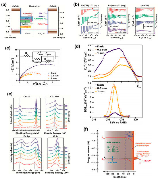
Figure 4.
(a) Schematic representation of the potential regions probed by the different redox couples shown next to the band position of CuFeO2. (b) LSV curves of CuFeO2. (c) Typical Nyquist plots representing EIS data for a CuFeO2 electrode, along with the equivalent circuit used to fit them. (d) Mott−Schottky plots of CuFeO2 electrodes and the corresponding density of surface states (DOS) extracted from Ctrap. (e) XPS spectra as a function of depth of Cu 2p, Cu LMM, Fe 2p, and O 1s. (f) Proposed energy band diagram for an isolated CuFeO2 electrode in the dark. Reprinted with permission from ref. [67], Copyright (2017), Chemistry of Materials.
In contrast, Hermans et al. [69] proposed that Fermi-level pinning at the Fe3+/Fe2+ electron polaron formation level intrinsically limits CuFeO2 from achieving a sufficient photovoltage. They argued that this is evidenced by the electronic and chemical properties of the CuFeO2–ITO and CuFeO2–H2O interfaces mapped by photoelectron spectroscopy (Figure 5). They concluded that Fermi level positions span across a wide range of 0.61 eV (see Figure 5c). This high degree of Fermi level tunability in CuFeO2 has a direct impact on its water reduction efficiency (see Figure 5a,b). The authors hypothesized that the observed Fermi-level pinning was not attributable to surface states but rather resulted from the formation and occupancy of the bulk Fe3+/Fe2+ polaron level and supported their assumption by similarities in octahedral Fe coordination in Fe2O3 [89] and CuFeO2, a consistent Fermi-level pinning position for various polytypes of CuFeO2 [67,71], and observations of similar charge transition levels in BiFeO3 at 0.7 eV vs. RHE [89,90]. Thus, the authors considered pinning at the Fe3+/Fe2+ charge transition level to be a prevalent phenomenon in iron-containing oxides. This can be considered an inherent challenge for CuFeO2, which is yet to be addressed by a suitable engineering solution.
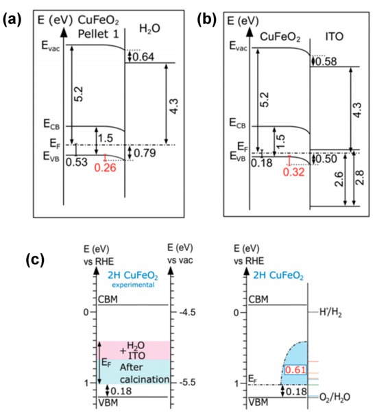
Figure 5.
Energy band diagrams of CuFeO2−H2O (a) and the CuFeO2−ITO (b) interface, revealing the Fermi level tunability in 2H CuFeO2 hexagonal nanoplatelet−shaped powder materials. (c) Corresponding summary of the experimental Fermi level ranges after interface formation (ITO or water). Reprinted with permission from ref. [69], Copyright (2020), Advanced Functional Materials.
3. Implemented Strategies for Improving Photoelectrochemical Performance of CuFeO2
Follow-up research aimed at addressing the limitations of CuFeO2 by engineering solutions to enhance the hydrogen evolution efficiencies of CuFeO2 photocathodes by (i) defect engineering, (ii) strategies to enhance light harvesting, or (iii) by heterojunction formation to improve charge separation. The overarching objective of defect engineering is to modulate the concentration of the (majority) charge carriers and to enhance conductivity through extrinsic or intrinsic doping. Secondly, enhancing light harvesting focuses on overcoming challenges such as limited visible light harvesting, low incident photon-to-current conversion efficiency (IPCE), and relatively weak absorption. Lastly, heterojunction formation aims at improving charge carrier separation while diminishing surface recombination. This approach is designed to address issues related to poor charge carrier transport, inadequate charge separation and transport, and the mitigation of unfavorable surface states. In the following sections, these strategies will be examined in detail, exploring their contribution to the enhancement of the efficiency of CuFeO2-based photocathodes in PEC water splitting applications.
3.1. Defect Engineering
The influence of oxygen intercalation by air treatment at 300 °C for 1 h on the photoelectrochemical properties of CuFeO2 thin films was first investigated by Prévot et al. [28]. The treatment was shown to result in a noticeable improvement in the photocurrents generated, with the best-performing electrode exhibiting a substantial increase in photocurrents, reaching 1.51 mA cm−2 at +0.35 V vs. RHE under front illumination and in oxygen-purged 1 M NaOH (Figure 6a). The enhancement was assigned to an increase in the acceptor density of the six-layer electrode after oxygen intercalation by approx. 20%. Annealing strategies were also investigated by Jang et al. [8]. In addition to conventional thermal annealing (CTA), hybrid microwave annealing (HMA) was shown to result in superior oxygen intercalation and partial oxidation of Cu+ to Cu2+. This process led to a more uniform distribution of Cu2+ while simultaneously inducing electron deficiency in Fe (Fe3+δ). The HMA-treated electrode exhibited the highest performance, achieving a cathodic photocurrent of −1.3 mA cm−2 at 0.4 VRHE, which is more than four times the performance of the unannealed CuFeO2 (Figure 6b). Furthermore, Mott–Schottky analysis (dark) revealed that the HMA-treated CuFeO2 electrode had the highest charge carrier density, which led to enhanced charge separation and carrier density, as also confirmed by XPS and XANES.
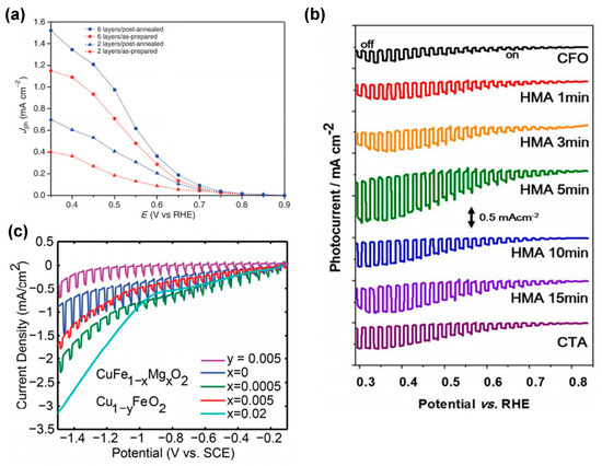
Figure 6.
(a) Photocurrent (total current minus dark current), Jph, as a function of applied potential for a six-layer CuFeO2 electrodes obtained in oxygen-saturated 1 M NaOH under one sun illumination before (red) and after (blue) post−annealing at 300 C in air. Reprinted with permission from ref. [71], Copyright (2015), ChemSusChem. (b) Current (J) -potential (V) curves of untreated CuFeO2, and post-treated CuFeO2 by CTA and HMA. Reprinted with permission from ref. [80], Copyright (2016), Chemistry of Materials. (c) Linear sweep voltammetry measurements of CuFe1-xMgxO2 and Cu1-yFeO2. Reprinted with permission from ref. [79], Copyright (2017), Materials Chemistry.
In addition to oxygen intercalation, cation doping and fabrication of Cu-deficient CuFeO2 electrodes are other common methods employed to increase the carrier concentration and conductivity of Cu-based photoelectrodes [93]. For instance, Wuttig et al. [79] sought to modulate the carrier concentration and thus the photoresponse of CuFeO2 photoelectrodes by Mg doping and Cu deficiency, as revealed by Hall effect measurements on pure, Mg-incorporated, and Cu-deficient pellets. The study revealed that pure CuFeO2 exhibited the lowest p-type carrier concentration and the highest carrier mobility, resulting in the largest photoresponse with a photocurrent of 0.43 mA/cm2 obtained under chopped light illumination (Figure 6c). The conductivity of CuFeO2 appeared to be limited by the delafossite defect chemistry, which changes the majority carrier type from p-type to n-type near the Mg solubility limit and at high Cu defect concentrations. The prevalence of n-type defects hinders the ability to achieve high p-type carrier densities, thereby emphasizing the delicate equilibrium between dopant concentrations, defect interactions, and material structure that governs the performance of CuFeO2 in PEC applications. In contrast, Jiang and collaborators [81] achieved a notable breakthrough by introducing more acceptor-type states, effectively increasing the concentration of p-type carriers using hydrothermal doping of Mg into CuFeO2. Their approach also bolstered the conductivity of CuFeO2, facilitating smoother carrier transport for photocathodes based on hexagonal CuFeO2 platelets. This advancement was accomplished through a straightforward method, hydrothermal doping of Mg into CuFeO2, yet with the optimal composition of 0.1% Mg, a CuFeO2 photocurrent density of only 100 μA cm−2 was obtained, and higher Mg-dopant concentrations led to a decline in photocurrent density.
3.2. Enhancing Light Harvesting
Overcoming the limitations of CuFeO2 delafossite photocathodes has also been addressed using strategies aimed at enhancing light absorption, reducing surface reflection by multiple scattering, and facilitating the formation of samples with a short carrier diffusion length. For example, an inverse opal (IO) nanostructure was proposed by Oh et al. [77] using an opal template and sol infiltration. In comparison with planar CuFeO2 photocathodes, the dimensionally ordered IO structure with a hexagonal skeleton and eight layers of a microporous structure (see Figure 7a) exhibits an evident absorption enhancement at 600–800 nm compared to planar CuFeO2 (see Figure 7b). IO-CuFeO2 photocathodes exhibited nearly twice the PEC performance of the planar CuFeO2, with a photocurrent density of 1.05 mA cm−2 at 0 V versus RHE.
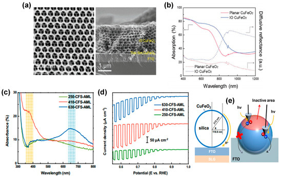
Figure 7.
(a) Top−view and cross−sectional SEM images of the IO−CuFeO2. (b) Absorption and diffusive reflectance of the planar and IO−CuFeO2 materials. Reprinted with permission from ref. [77], Copyright (2019), Advanced Functional Materials. (c) Absorbance spectra of a CFS−AML photocathodes. (d) LSV of CFS−AML photocathode. Reprinted with permission from ref. [84], Copyright (2017), ACS Applied Materials & Interfaces. (e) Schematic image of the maximum travel length of the majority carriers.
Oh et al. [84] also developed transparent CuFeO2 photoelectrodes showing comparable photocurrent with thin film-based photoelectrodes using an innovative architecture composed of two-dimensional silica microsphere photonic crystals (2D PC) decorated with a thin CuFeO2 layer. The concept facilitates the establishment of a diverse range of PC systems, each exhibiting a distinct absorption range. These absorption ranges are attributed to the periodic arrangement of distinct refractive index materials, with the photonic stop band (PSB) of each system contingent on the diameter of the microspheres (see Figure 7c). As pointed out by Oh et al., 2D PC systems containing microspheres@CuFeO2 with a diameter of 550 nm would likely facilitate the generation of higher photocurrents. This is due to the more favorable location of their PSB, which would allow for better utilization of incoming photons and collection of photogenerated carriers. In conclusion, the research conducted by Oh et al. indicates that CuFeO2-decorated microsphere photocathodes, characterized by their visible light transmittance (76.4%), maintain the capacity for photo-current generation (0.2 mA cm⁻2 at 0.6 V vs. RHE, refer to Figure 7d). This property enables their integration with small band gap semiconductors within a tandem device configuration [94].
3.3. Improving Charge Carrier Separation by Heterojunction Formation
The formation of heterojunctions to increase the charge separation of photogenerated charge carriers is often proposed in combination with other strategies. For example, Jang et al. [80] used HMA-treated CuFeO2 electrodes for coupling with a hydrogen evolution reaction (HER) electrocatalyst onto its surface. The authors particularly used nickel-iron layered double hydroxide (NiFe LDH) prepared by a one-step hydrothermal method and deposited on HMA-CuFeO2 photocathodes (HMA-NiFe). Additionally, a combination of NiFe LDH and reduced graphene oxide (HMA-NiFe/rGO) was investigated. Both modifications (Figure 8a) led to drastic improvements in photocurrent generation up to −2.4 mA cm−2 at 0.4 VRHE, being a 7–8 fold and 1.5–2 fold increase for HMA-NiFe/rGO relative to unannealed CuFeO2 and HMA-CuFeO2 photocathodes, respectively. Oh et al. [77] modified IO-CuFeO2 and planar CuFeO2 photocathodes with a CoFe LDH catalyst and a C60 layer, respectively. The determined photocurrent density of −4.86 mA cm−2 at 0 V vs. RHE (Figure 8b) was shown to be a factor of 2 larger than the HER performance of the planar CuFeO2/C60/CoFe LDH photocathode. IPCE measurements revealed that the IO-CuFeO2-based photocathode exhibited a high IPCE value of 17.5% at 600 nm due to both increased light absorption and enhanced charge transfer/extraction.
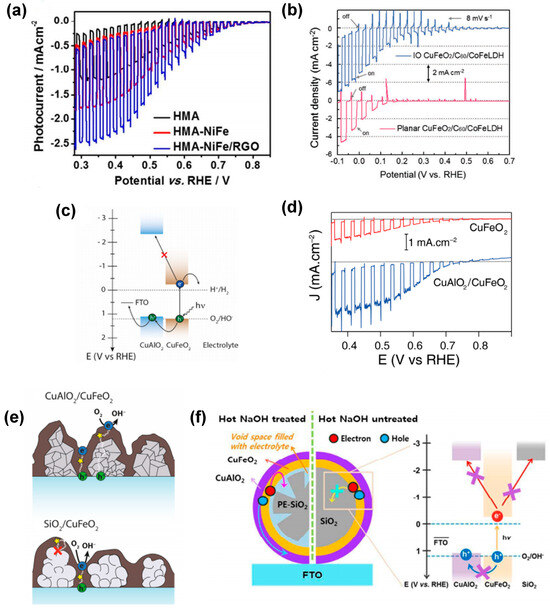
Figure 8.
(a) J−V curves of HMA, HMA−NiFe, and HMA−NiFe/RGO. Reprinted with permission from ref. [80], Copyright (2016), Chemistry of Materials. (b) Linear sweep voltammograms of the IO and planar CuFeO2 photocathodes after modification by the electrocatalyst. Reprinted with permission from ref. [77], Copyright (2019), Advanced Functional Materials. (c) Simplified energy diagram of the host−guest CuAlO2/CuFeO2 electrode. (d) Comparison of J−V curves obtained for optimized CuAlO2/CuFeO2 (blue trace) and CuFeO2 (red trace) electrodes. Reprinted with permission from ref. [68], Copyright (2016), Materials Chemistry. (e) Scheme of the possible pathways that photogenerated charges can take inside CuAlO2/CuFeO2 and SiO2/CuFeO2 electrodes. Reprinted with permission from ref. [83], Copyright (2018), Nanoscale. (f) Schematic illustration of the electron transfer pathways at the CuFeO2−electrolyte interface for 2D opal-based photocathodes.
As highlighted above, the high density of surface states within nano-sized CuFeO2 is assumed to enhance recombination of photoexcited electrons. To address this problem, Aqaei et al. [82] introduced a diamond-like carbon (DLC) scaffold with plasmonic gold (Au) nanoparticles (NPs) atop CuFeO2. These Au@DLC/CuFeO2 samples were fabricated using RF-sputtering and RF-Plasma Enhanced Chemical Vapor Deposition (PECVD); however, only a minor improvement in the PEC performance of CuFeO2 was revealed, which was assigned to the passivation of electron traps.
The challenge of reconciling minority carrier transport and light absorption has been a central concern in enhancing the performance of various photoelectrodes, including hematite photoanodes. Host-guest approaches, in which an ultra-thin layer of the light absorber is deposited onto a high surface area scaffold with suitable electronic properties, have been shown to address this issue effectively. This approach is well-known for its ability to facilitate the decoupling of light absorption and charge transfer. This, in turn, has been shown to mitigate charge carrier recombination, thus leading to enhanced photocurrents [95,96]. Applying this approach to CuFeO2 requires identification of a p-type material fulfilling four fundamental criteria: possessing (1) a high transparency as observed for wide band gap (large Eg) materials; (2) substantial p-type (hole) conductivity; (3) valence and conduction band energy levels exceeding those of CuFeO2 to impede back electron transfer and facilitate the efficient transfer of holes from the absorber to the scaffold; (4) high stability under the conditions required for CuFeO2 preparation and for PEC testing. Prévot et al. [68] and Oh et al. [83] successfully applied the host-guest composite electrode strategy to CuFeO2 photoanodes using a p-type CuAlO2 scaffold. Indeed, the optoelectronic properties of CuAlO2 (Figure 8c) have been demonstrated to be advantageous, in accordance with its visible light transparency (Eg = 3.5 eV) and a flat band potential that is 0.1 eV higher than that of CuFeO2. Given this offset, a selective extraction of photogenerated holes towards the substrate at the CuFeO2–CuAlO2 interface is predicted. The thickness of the host and guest layers was independently varied, thus enabling the successful fabrication of a host-guest electrode on a 2 µm CuAlO2 scaffold that contains approximately 2.2 times more CuFeO2 than the most efficient bare CuFeO2 electrode (prepared directly on FTO) [68]. Using the scaffold layer with a thickness of 2 µm resulted in a 2.4-fold increase in photocurrent density in the presence of O2 as a sacrificial electron scavenger compared to bare CuFeO2, i.e., a photocurrent density of 2.4 mA cm−2 at +0.4 V vs. RHE (Figure 8d) was obtained. A comparison of the host-guest strategy with CuFeO2 layers prepared on an insulating SiO2 scaffold further suggested that CuAlO2 facilitated improved charge transport rather than merely decreasing recombination rates when compared to the CuFeO2 film alone (Figure 8e). In addition, the host-guest approach was also combined with the transparent 2D opal photocathode system [84]. By introducing a double-shelled heterojunction configuration with inner CuFeO2 and outer CuAlO2 shells on silica microsphere scaffolds [83], efficient charge transfer (Figure 8f) and a 9-fold enhancement in photoresponse in comparison to single-shelled counterparts were achieved. In this design, issues related to the blockage of electrolyte were mitigated by the design of a photoelectrode based on partially etched silica microspheres (PE-SiO2).
4. Fermi-Level Pinning in CuFeO2: Lessons from Other Photoelectrodes
The upper limits of the Fermi energy in CuFeO2 have been determined to be approximately 0.8 eV [69], thus indicating a relatively constrained range for a material that possesses a 1.5 eV band gap (Figure 3b). This limitation impacts the photovoltage of a photocathode, as it is dictated by the splitting of the quasi-Fermi levels at the electron–hole contacts. To fully harness the band gap potential of CuFeO2 for water splitting, it is necessary to develop a more profound understanding of Fermi-level pinning phenomena in CuFeO2 and other materials, as well as strategies to mitigate it. This section focuses on elucidating both intrinsic contributions and other mechanisms of Fermi-level pinning in materials like CuFeO2 and their implications for optimizing performance. To clarify, intrinsic contributions to Fermi-level pinning are inherent to the material itself. These include phenomena such as Metal-Induced Gap States (MIGS) and electrochemical changes within the semiconductor, which arise from its fundamental structure and bonding. In contrast, other mechanisms involve external factors, such as crystallographic defects or foreign atoms introduced during material processing, which can alter the electronic properties. Differentiating between these contributions is key to developing targeted strategies for mitigating Fermi-level pinning and improving the PEC performance of CuFeO2.
4.1. Intrinsic Contributions to Fermi-Level Pinning
Interface states affecting the barrier height can emerge even at defect-free surfaces when interfaces between semiconductors and metals, as well as at interfaces between two semiconductors, are established. A metal in contact with the surface of a semiconductor results in an overlap of the wave function of valence electrons of the semiconductor and the metal, thereby aligning their Fermi levels. This alignment gives rise to gap states known as Metal-Induced Gap States (MIGS), which penetrate deeper into the semiconductor and are responsible for pinning the surface energy state, irrespective of the type of metal used [97,98]. These MIGS play a crucial role in Fermi-level pinning (FLP) and facilitate electron and hole tunneling into the semiconductor [99]. The barriers for tunneling at semiconductor–metal interfaces are determined by the Schottky barriers for electrons and holes, while for semiconductor heterojunctions, they are defined by the valence and conduction band offsets, respectively. The nature of interface states is dependent on the character of the chemical bond developed between constituent atoms; ionic materials display little or no Fermi-level stabilization at the interface, while covalent materials display virtually complete stabilization [100,101]. This phenomenon suggests a dependence on the electronegativity of the metal, reflecting the local charge transfer related to the chemical bonds at the semiconductor–metal interface, rather than relying on specific surface properties of the metal. Therefore, the degree of Fermi-level pinning is often characterized in terms of an index of interface behavior S, defined as follows:
where represents Schottky barrier heights and is the electronegativity of the metal forming the barrier.
The index of interface behavior S is small for strong Fermi-level pinning, a characteristic notably pronounced in semiconductors with strong covalent bonding character [102]. This is evident in elemental semiconductors such as carbon (C), silicon (Si), germanium (Ge), and group III–V compounds like gallium arsenide (GaAs) and others, where S is approximately 0.1. Conversely, semiconductors with more ionic bonds typically exhibit weaker Fermi-level pinning, with S around 1.
In addition to Metal-Induced Gap States (MIGS), electrochemical reduction or oxidation of a material is another intrinsic contributor responsible for FLP [103]. These valence changes of cationic or anionic species effectively constrain the Fermi energy within a material, as the respective concentration of the defects is equal to that of the atoms. Recently, Suzuki et al. [104] demonstrated limited Fermi shifts in β-CuGaO2 to ∼0.8 eV, significantly smaller than its band gap of 1.5 eV. The origin of the Fermi-level pinning, similar to that observed at Cu2O–ZnO interfaces [105], is related to the electrochemical oxidation/reduction of Cu. Observations of upper limits of the Fermi energy have also been made in Fe2O3 [89], BiFeO3 [90], and BiVO4 [106], where direct spectroscopic evidence for the reduction of Fe or V was obtained. In the case of CuFeO2, the electrochemical reduction of Fe, which corresponds to a valence change from Fe3+ to Fe2+, is anticipated to constitute a fundamental constraint on the Fermi level energy.
4.2. Other Mechanisms Contributing to Fermi-Level Pinning
Crystallographic defects can also induce Fermi-level pinning, with point defects being a typical example that induce Fermi-level pinning in ionic compounds. For instance, oxygen vacancies in ZnO form deep donor states [107,108], while copper vacancies in CuGaSe2 contribute to self-compensation defects [109]. Moreover, extrinsic states such as crystallographic defects (point defects and dislocations) can impact barrier heights at semiconductor–metal interfaces [110]. This influence can arise from factors like lattice mismatch [111] or chemical reactions during interface formation. For instance, the oxygen content at the semiconductor–metal interface can vary significantly [112], and the deposition of metals onto semiconductor surfaces can lead to defect formation due to the release of heat during condensation. Rao et al. [113] calculated the heat of condensation of Pt onto BaTiO3 to be approximately 4 eV, a value exceeding the energy required to create oxygen vacancies in most conducting oxides. This contrasts with the energy required to create oxygen vacancies in conducting oxides, which varies depending on the specific material. For example, in BiFeO3, the oxygen vacancy energy level is calculated to be 0.6 eV below the conduction band edge [114]. These defects are likely to be controlled through careful selection of contact materials and processing techniques during interface fabrication. Their concentration can be adjusted through post-deposition treatments, such as annealing oxide–metal interfaces in oxidizing atmospheres which increases the barrier height for electrons, whereas reducing atmospheres result in a lower barrier. These changes in barrier height, which can be substantial (up to 1 eV), may occur even at room temperature, particularly with catalytically active contact metals like Pt. For example, photoelectron spectra of a SnO2 surface coated with a ~2 nm Pt film show a fully oxidized surface when exposed to an oxygen atmosphere, while metallic Sn species occur under vacuum. This reversible switching between oxidized and reduced states demonstrates the potential for controlling interface properties through atmospheric manipulation, as shown in Figure 9 [115].
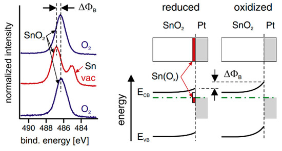
Figure 9.
(Left) Sn 3d photoelectron spectra recorded from a polycrystalline SnO2 thin film coated with ~2 nm Pt. (Right) Energy band diagrams and schematic interface chemical structures of oxidized and reduced SnO2–Pt interfaces. Reprinted with permission from ref. [115], Copyright (2012), Thin Solid Films.
5. Suggested Strategies for Enhancing CuFeO2 PEC Performance
In Section 3, we provided a comprehensive review of the strategies that have been implemented to enhance CuFeO2 photocathodes. These strategies encompass defect engineering, improving light harvesting, and utilizing heterojunctions. However, as discussed in Section 4, the primary challenge for CuFeO2 photocathodes is Fermi-level pinning (FLP), which limits the material’s performance in photoelectrochemical (PEC) applications. To address this challenge, it is essential to explore strategies that specifically target FLP mitigation. In this section, we present three potential strategies to enhance the PEC performance of CuFeO2.
Recent research focusing on the integration of mediators such as conductive polymers, metal nanoparticles, or molecular catalysts into selective contacts for photocathodes represents a notable advancement in the field [116]. These mediators can enhance charge transfer, facilitate electron or hole transport, and improve overall efficiency in PEC applications. While previous studies have examined hole or electron selective contacts individually, integration of both types of contact has thus far not been reported. Notably, the integration of a hole-selective contact between FTO and CuFeO2, which is essential for impeding back electron transfer and facilitating hole transfer to FTO, is a significant development. Additionally, the integration of an electron-selective contact between CuFeO2 and the catalyst or electrolyte, aimed at enhancing charge transfer and overcoming the hindrance posed by the high density of surface states within CuFeO2, is noteworthy. These integrated systems, driven by electrochemical potential gradients and employing multimediators, hold immense promise for significantly enhancing charge separation and transportation (Figure 10).
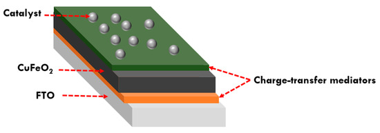
Figure 10.
Schematic representation of an integrated CuFeO2-based photocathode design.
Despite the fact that CuFeO2 has already been shown to exhibit favorable charge transport properties (see Table 3) in comparison to other photoelectrodes, electrochemical impedance spectroscopy (EIS) measurements further support the substantial impact of selective contacts [117]. It is therefore concluded that such advancements have the potential to lead to improved overall performance in the performance of Cu delafossite photoelectrodes.
Table 3.
Overview of relevant parameters of the EIS measurements on CuFeO2-based photocathodes.
Addressing the substrate’s role as a current collector is another critical factor, particularly given that the majority of reported CuFeO2 photocathodes deposit CuFeO2 directly onto FTO substrates. However, existing literature indicates the inactivity of iron-containing metal oxide films during operation caused by direct interaction and interface formation with fluorine-doped tin oxide (FTO) [118,119]. For instance, in hematite films like α-Fe2O3, this interaction widens Fe 3d−O 2p hybridized states. This has been shown to result in decreased p-d orbital hybridization and increased recombination of photogenerated charge carriers [120,121,122]. Furthermore, photoelectrochemical losses have been linked to the low degree of crystallinity of deposited iron-containing metal oxides on FTO, which correlates with the degree of light absorption and photoelectrochemical water oxidation performance [123,124]. These findings suggest that interfacial layers between the absorber and current collector significantly impact electrode assembly transport properties. To overcome these drawbacks, exploring alternative current collectors such as copper (Cu), graphene, or conductive polymers represents a promising avenue for enhancing photoelectrode performance. For instance, copper has been utilized due to its excellent electrical conductivity and compatibility with various semiconductor materials [125]. Research by Fu et al. demonstrated that using graphene as a current collector improved charge transport and reduced recombination losses in CuFeO2-based photocathodes [86]. Additionally, the integration of a buffer layer, such as titanium dioxide (TiO2) or zinc oxide (ZnO), between the FTO substrate and the iron-containing metal oxide can significantly enhance performance. Recent studies have demonstrated that incorporating a TiO2 buffer layer improved the crystallinity and light absorption of α-Fe2O3 films, leading to enhanced photocatalytic activity [126].
If the hypothesis that the constraint Fermi level energy is caused by electro-chemical reduction of Fe is correct, then the full utilization of CuFeO2′s band gap as a photocathode may prove challenging. In such a scenario, it becomes necessary to explore alternative mechanisms for charge separation, moving away from conventional approaches such as p-n junctions or heterojunctions, which are limited by the electronic bandgap of the semiconductor. One promising avenue involves the exploitation of the ferroelectric property of CuFeO2. In this context, Yang et al. [127] have demonstrated the role of ferroelectric domain walls in enhancing charge separation and generating a larger photovoltage in BiFeO3 thin films. Their findings revealed significant differences in photovoltaic behavior depending on the orientation of domain walls relative to the electrodes, resulting in notably higher photovoltages than the bandgap alone would suggest. They emphasize the importance of controlling the domain structure in BiFeO3 films by growing them on annealed and un-annealed DyScO3 (DSO) substrates. Additionally, they demonstrate that the photovoltaic effect can be controlled by applying electric fields to induce ferroelectric domain switching, creating a system with perpendicular domain walls and enhancing the photovoltaic effect.
6. Concluding Remarks
In the context of photoelectrochemical water splitting, Cu-based metal oxide photocathodes, notably CuFeO2, have emerged as a prominent class of materials due to their advantageous properties, including narrow bandgaps, cost-effectiveness, and favorable band-edge positions that are conducive to water splitting. CuFeO2 is notable for its responsiveness to visible light, exhibiting multi-band absorption and an anticipated high photovoltage owing to its theoretical Fermi level positioned at 1.5 V vs. RHE. However, despite these promising properties, unprotected CuFeO2 photocathodes face significant challenges, including exceptionally low photocurrent and difficulties in effectively driving hydrogen production during water reduction. A primary challenge in addressing this issue is the difficulty in synthesizing high-quality, pure-phase CuFeO2 on FTO substrates, which can be attributed to the inherent complexities of the Cu–Fe–O system, leading to the formation of undesirable phases. Furthermore, the presence of bulk or interface defects, situated approximately 0.35 eV above the flat band potential, leads to Fermi-level pinning at the semiconductor–liquid junction. This pinning significantly restricts the photovoltage of bare CuFeO2 to 0.35 V. This limitation poses a major obstacle to the advancement of unbiased tandem devices incorporating CuFeO2 photocathodes, necessitating substantial enhancements in CuFeO2′s photovoltage. This review comprehensively explores recent advancements in earth-abundant CuFeO2 photocathode design, offering insights into the current understanding of key factors diminishing the STH efficiencies, such as Fermi-level pinning, and pointing out potential strategies to overcome these challenges, among which we consider careful design of hole and electron mediator layers as being most promising, all with the aim of advancing the potential of CuFeO2 as a practical material for PEC water splitting for solar hydrogen production.
Author Contributions
Conceptualization, M.E.I. and B.M.; writing—original draft preparation, M.E.I.; writing—review and editing, M.E.I., B.M., M.A.-L. and L.A.; supervision, B.M., M.A.-L. and L.A.; funding acquisition, M.E.I. and L.A. All authors have read and agreed to the published version of the manuscript.
Funding
This research was funded by German Academic Exchange Service (DAAD “ERA Fellowships—Green Hydrogen”) grant number No. 57685697 and by Agence nationale de la recherche (ANR) grant number ANR-22-LERE-0004. The APC was waived.
Data Availability Statement
No new data were created or analyzed in this study.
Acknowledgments
We would like to thank The DAAD scholarship program “ERA Fellowships—Green Hydrogen” for their support. M. El Idrissi would like to thank the LEAP RE initiative, founded by the Ministry of Higher Education, Scientific Research, and Innovation (MESRSI), for financial support through the project “Environmentally friendly colloidal quantum dots for high performance solar cells”/(QDSOC).
Conflicts of Interest
The authors declare no conflict of interest.
Abbreviations
The following abbreviations are used in this manuscript:
| PEC | Photoelectrochemical |
| IPCE | Incident Photon-to-Current Efficiency |
| HER | Hydrogen Evolution Reaction |
| OER | Oxygen Evolution Reaction |
| STH | Solar-to-Hydrogen |
| EIS | Electrochemical Impedance Spectroscopy |
| TRMC | Time-Resolved Microwave Conductivity |
| MS | Mott–Schottky |
| KPFM | Kelvin Probe Force Microscopy |
| XPS | X-Ray Photoelectron Spectroscopy |
| HMA | Hybrid Microwave Annealing |
| CTA | Conventional Thermal Annealing |
| LDH | Layered Double Hydroxide DLC |
| DLC | Diamond-Like Carbon |
| NPs | Nanoparticles |
| PSB | Photonic Stop Band |
| FLP | Fermi Level Pinning |
| MIGS | Metal-Induced Gap States |
| FTO | Fluorine-Doped Tin Oxide |
| TiO2 | Titanium Dioxide |
| ZnO | Zinc Oxide |
| DSO | DyScO3 |
| CFO | CuFeO2 |
References
- Tee, S.Y.; Win, K.Y.; Teo, W.S.; Koh, L.-D.; Liu, S.; Teng, C.P.; Han, M.-Y. Recent Progress in Energy-Driven Water Splitting. Adv. Sci. 2017, 4, 1600337. [Google Scholar] [CrossRef] [PubMed]
- Ryu, J.; Jang, Y.J.; Choi, S.; Kang, H.J.; Park, H.; Lee, J.S.; Park, S. All-in-one synthesis of mesoporous silicon nanosheets from natural clay and their applicability to hydrogen evolution. NPG Asia Mater. 2016, 8, e248. [Google Scholar] [CrossRef]
- Jang, Y.J.; Ryu, J.; Hong, D.; Park, S.; Lee, J.S. A multi-stacked hyperporous silicon flake for highly active solar hydrogen production. Chem. Commun. 2016, 52, 10221–10224. [Google Scholar] [CrossRef]
- Jang, Y.J.; Lee, J.; Lee, J.; Lee, J.S. Solar Hydrogen Production from Zinc Telluride Photocathode Modified with Carbon and Molybdenum Sulfide. ACS Appl. Mater. Interfaces 2016, 8, 7748–7755. [Google Scholar] [CrossRef]
- Guan, D.; Wang, B.; Zhang, J.; Shi, R.; Jiao, K.; Li, L.; Wang, Y.; Xie, B.; Zhang, Q.; Yu, J.; et al. Hydrogen society: From present to future. Energy Environ. Sci. 2023, 16, 4926–4943. [Google Scholar] [CrossRef]
- Iqbal, M.Z.; Siddique, S.; Khan, A.; Haider, S.S.; Khalid, M. Recent developments in graphene based novel structures for efficient and durable fuel cells. Mater. Res. Bull. 2020, 122, 110674. [Google Scholar] [CrossRef]
- Peerakiatkhajohn, P.; Yun, J.-H.; Wang, S.; Wang, L. Review of recent progress in unassisted photoelectrochemical water splitting: From material modification to configuration design. J. Photon. Energy 2016, 7, 12006. [Google Scholar] [CrossRef]
- Youn, D.H.; Park, Y.B.; Kim, J.Y.; Magesh, G.; Jang, Y.J.; Lee, J.S. One-pot synthesis of NiFe layered double hydroxide/reduced graphene oxide composite as an efficient electrocatalyst for electrochemical and photoelectrochemical water oxidation. J. Power Source 2015, 294, 437–443. [Google Scholar] [CrossRef]
- Breyer, C.; Lopez, G.; Bogdanov, D.; Laaksonen, P. The role of electricity-based hydrogen in the emerging power-to-X economy. Int. J. Hydrogen Energy 2024, 49, 351–359. [Google Scholar] [CrossRef]
- Ke, G.-L.; Jia, B.; He, H.-C.; Zhou, Y.; Zhou, M. State-of-the-art advancements of transition metal oxides as photoelectrode materials for solar water splitting. Rare Met. 2022, 41, 2370–2386. [Google Scholar] [CrossRef]
- Domenichini, R.; Gallio, M.; Lazzaretto, A. Combined production of hydrogen and power from heavy oil gasification: Pinch analysis, thermodynamic and economic evaluations. Energy 2010, 35, 2184–2193. [Google Scholar] [CrossRef]
- Stiegel, G.J.; Ramezan, M. Hydrogen from coal gasification: An economical pathway to a sustainable energy future. Int. J. Coal Geol. 2006, 65, 173–190. [Google Scholar] [CrossRef]
- Ni, M.; Leung, D.Y.; Leung, M.K.; Sumathy, K. An overview of hydrogen production from biomass. Fuel Process. Technol. 2006, 87, 461–472. [Google Scholar] [CrossRef]
- Wang, M.; Wang, Z.; Gong, X.; Guo, Z. The intensification technologies to water electrolysis for hydrogen production—A review. Renew. Sust. Energ. Rev. 2014, 29, 573–588. [Google Scholar] [CrossRef]
- BALL, M.; WIETSCHEL, M. The future of hydrogen—opportunities and challenges. Int. J. Hydrogen Energy 2009, 34, 615–627. [Google Scholar] [CrossRef]
- Holladay, J.D.; Hu, J.; King, D.L.; Wang, Y. An overview of hydrogen production technologies. Catal. Today 2009, 139, 244–260. [Google Scholar] [CrossRef]
- Damyanova, S.; Pawelec, B.; Arishtirova, K.; Fierro, J. Ni-based catalysts for reforming of methane with CO2. Int. J. Hydrogen Energy 2012, 37, 15966–15975. [Google Scholar] [CrossRef]
- Chen, S.; Takata, T.; Domen, K. Particulate photocatalysts for overall water splitting. Nat. Rev. Mater. 2017, 2, 17050. [Google Scholar] [CrossRef]
- Kelly, N.; Gibson, T.; Ouwerkerk, D. A solar-powered, high-efficiency hydrogen fueling system using high-pressure electrolysis of water: Design and initial results. Int. J. Hydrogen Energy 2008, 33, 2747–2764. [Google Scholar] [CrossRef]
- Sivula, K. Toward Economically Feasible Direct Solar-to-Fuel Energy Conversion. J. Phys. Chem. Lett. 2015, 6, 975–976. [Google Scholar] [CrossRef]
- Chen, Q.; Fan, G.; Fu, H.; Li, Z.; Zou, Z. Tandem photoelectrochemical cells for solar water splitting. Adv. Phys. X 2018, 3, 1487267. [Google Scholar] [CrossRef]
- Walter, M.G.; Warren, E.L.; McKone, J.R.; Boettcher, S.W.; Mi, Q.; Santori, E.A.; Lewis, N.S. Solar water splitting cells. Chem. Rev. 2010, 110, 6446–6473. [Google Scholar] [CrossRef]
- Mei, B.; Wenderich, K. Principles and Limitations of Photoelectrochemical Fuel Generation. In Heterogeneous Photocatalysis; Strunk, J., Ed.; Wiley: Hoboken, NJ, USA, 2021; pp. 77–100. ISBN 9783527344642. [Google Scholar]
- Mei, B.; Mul, G.; Seger, B. Beyond Water Splitting: Efficiencies of Photo-Electrochemical Devices Producing Hydrogen and Valuable Oxidation Products. Adv. Sustain. Syst. 2017, 1, 1600035. [Google Scholar] [CrossRef]
- Moriya, M.; Minegishi, T.; Kumagai, H.; Katayama, M.; Kubota, J.; Domen, K. Stable hydrogen evolution from CdS-modified CuGaSe2 photoelectrode under visible-light irradiation. J. Am. Chem. Soc. 2013, 135, 3733–3735. [Google Scholar] [CrossRef]
- Sullivan, I.; Zoellner, B.; Maggard, P.A. Copper(I)-Based p-Type Oxides for Photoelectrochemical and Photovoltaic Solar Energy Conversion. Chem. Mater. 2016, 28, 5999–6016. [Google Scholar] [CrossRef]
- Li, C.; Hisatomi, T.; Watanabe, O.; Nakabayashi, M.; Shibata, N.; Domen, K.; Delaunay, J.-J. Positive onset potential and stability of Cu2O-based photocathodes in water splitting by atomic layer deposition of a Ga2O3 buffer layer. Energy Environ. Sci. 2015, 8, 1493–1500. [Google Scholar] [CrossRef]
- Read, C.G.; Park, Y.; Choi, K.-S. Electrochemical Synthesis of p-Type CuFeO2 Electrodes for Use in a Photoelectrochemical Cell. J. Phys. Chem. Lett. 2012, 3, 1872–1876. [Google Scholar] [CrossRef]
- Sathre, R.; Scown, C.D.; Morrow, W.R.; Stevens, J.C.; Sharp, I.D.; Ager, J.W.; Walczak, K.; Houle, F.A.; Greenblatt, J.B. Life-cycle net energy assessment of large-scale hydrogen production via photoelectrochemical water splitting. Energy Environ. Sci. 2014, 7, 3264–3278. [Google Scholar] [CrossRef]
- Li, Z.; Fang, S.; Sun, H.; Chung, R.-J.; Fang, X.; He, J.-H. Solar Hydrogen. Adv. Energy Mater. 2023, 13, 2203019. [Google Scholar] [CrossRef]
- Zhao, X.; Hu, J.; Yao, X.; Chen, S.; Chen, Z. Clarifying the Roles of Oxygen Vacancy in W-Doped BiVO4 for Solar Water Splitting. ACS Appl. Energy Mater. 2018, 1, 3410–3419. [Google Scholar] [CrossRef]
- Fujishima, A.; Honda, K. Electrochemical Photolysis of Water at a Semiconductor Electrode. Nature 1972, 238, 37–38. [Google Scholar] [CrossRef]
- Mei, B.; Seger, B.; Pedersen, T.; Malizia, M.; Hansen, O.; Chorkendorff, I.; Vesborg, P.C.K. Protection of p+-n-Si Photoanodes by Sputter-Deposited Ir/IrOx Thin Films. J. Phys. Chem. Lett. 2014, 5, 1948–1952. [Google Scholar] [CrossRef] [PubMed]
- Subramanyam, P.; Naresh Kumar, P.; Deepa, M.; Subrahmanyam, C.; Ghosal, P. Bismuth sulfide nanocrystals and gold nanorods increase the photovoltaic response of a TiO2/CdS based cell. Sol. Energy Mater. Sol. Cells 2017, 159, 296–306. [Google Scholar] [CrossRef]
- Subramanyam, P.; Vinodkumar, T.; Nepak, D.; Deepa, M.; Subrahmanyam, C. Mo-doped BiVO4@reduced graphene oxide composite as an efficient photoanode for photoelectrochemical water splitting. Catal. Today 2019, 325, 73–80. [Google Scholar] [CrossRef]
- Subramanyam, P.; Meena, B.; Sinha, G.N.; Deepa, M.; Subrahmanyam, C. Decoration of plasmonic Cu nanoparticles on WO3/Bi2S3 QDs heterojunction for enhanced photoelectrochemical water splitting. Int. J. Hydrogen Energy 2020, 45, 7706–7715. [Google Scholar] [CrossRef]
- Subramanyam, P.; Meena, B.; Suryakala, D.; Deepa, M.; Subrahmanyam, C. Plasmonic nanometal decorated photoanodes for efficient photoelectrochemical water splitting. Catal. Today 2021, 379, 1–6. [Google Scholar] [CrossRef]
- Li, J.; Cushing, S.K.; Zheng, P.; Senty, T.; Meng, F.; Bristow, A.D.; Manivannan, A.; Wu, N. Solar hydrogen generation by a CdS-Au-TiO2 sandwich nanorod array enhanced with Au nanoparticle as electron relay and plasmonic photosensitizer. J. Am. Chem. Soc. 2014, 136, 8438–8449. [Google Scholar] [CrossRef]
- van Benthem, K.; Elsässer, C.; French, R.H. Bulk electronic structure of SrTiO3: Experiment and theory. J. Appl. Phys. 2001, 90, 6156–6164. [Google Scholar] [CrossRef]
- Aadenan, A.; Arzaee, N.A.; Rahman, N.A.A.; Noh, M.F.M.; Daud, M.N.M.; Mohamed, N.A.; Mustapha, M.; Ibrahim, M.A.; Ludin, N.A.; Teridi, M.A.M. Effect of aqueous media on photoelectrochemical water splitting performance of α-Fe2O3/LaFeO3:Cr tandem cell. J. Mater. Res. 2024, 39, 737–749. [Google Scholar] [CrossRef]
- Shi, H.; Guo, H.; Wang, S.; Zhang, G.; Hu, Y.; Jiang, W.; Liu, G. Visible Light Photoanode Material for Photoelectrochemical Water Splitting: A Review of Bismuth Vanadate. Energy Fuels 2022, 36, 11404–11427. [Google Scholar] [CrossRef]
- Fan, R.; Mi, Z.; Shen, M. Silicon based photoelectrodes for photoelectrochemical water splitting. Opt. Express 2019, 27, A51–A80. [Google Scholar] [CrossRef]
- Luo, Z.; Wang, T.; Gong, J. Single-crystal silicon-based electrodes for unbiased solar water splitting: Current status and prospects. Chem. Soc. Rev. 2019, 48, 2158–2181. [Google Scholar] [CrossRef] [PubMed]
- Lee, M.H.; Takei, K.; Zhang, J.; Kapadia, R.; Zheng, M.; Chen, Y.-Z.; Nah, J.; Matthews, T.S.; Chueh, Y.-L.; Ager, J.W.; et al. p-Type InP nanopillar photocathodes for efficient solar-driven hydrogen production. Angew. Chem. Int. Ed Engl. 2012, 51, 10760–10764. [Google Scholar] [CrossRef] [PubMed]
- Su, J.; Minegishi, T.; Kageshima, Y.; Kobayashi, H.; Hisatomi, T.; Higashi, T.; Katayama, M.; Domen, K. CdTe-Based Photoanode for Oxygen Evolution from Water under Simulated Sunlight. J. Phys. Chem. Lett. 2017, 8, 5712–5717. [Google Scholar] [CrossRef] [PubMed]
- Jacobsson, T.J.; Platzer-Björkman, C.; Edoff, M.; Edvinsson, T. CuInxGa1−xSe2 as an efficient photocathode for solar hydrogen generation. Int. J. Hydrogen Energy 2013, 38, 15027–15035. [Google Scholar] [CrossRef]
- Kobayashi, H.; Sato, N.; Orita, M.; Kuang, Y.; Kaneko, H.; Minegishi, T.; Yamada, T.; Domen, K. Development of highly efficient CuIn0.5Ga0.5Se2 -based photocathode and application to overall solar driven water splitting. Energy Environ. Sci. 2018, 11, 3003–3009. [Google Scholar] [CrossRef]
- Zhao, J.; Minegishi, T.; Zhang, L.; Zhong, M.; Gunawan; Nakabayashi, M.; Ma, G.; Hisatomi, T.; Katayama, M.; Ikeda, S.; et al. Enhancement of solar hydrogen evolution from water by surface modification with CdS and TiO2 on porous CuInS2 photocathodes prepared by an electrodeposition-sulfurization method. Angew. Chem. Int. Ed. Engl. 2014, 53, 11808–11812. [Google Scholar] [CrossRef]
- Muzzillo, C.P.; Klein, W.E.; Li, Z.; DeAngelis, A.D.; Horsley, K.; Zhu, K.; Gaillard, N. Low-Cost, Efficient, and Durable H2 Production by Photoelectrochemical Water Splitting with CuGa3Se5 Photocathodes. ACS Appl. Mater. Interfaces 2018, 10, 19573–19579. [Google Scholar] [CrossRef]
- Takayama, T.; Iwase, A.; Kudo, A. Enhancing Photocathodic Performances of Particulate-CuGaS2-Based Photoelectrodes via Conjugation with Conductive Organic Polymers for Efficient Solar-Driven Hydrogen Production and CO2 Reduction. ACS Appl. Mater. Interfaces 2024, 16, 36423–36432. [Google Scholar] [CrossRef]
- Zhang, L.; Minegishi, T.; Nakabayashi, M.; Suzuki, Y.; Seki, K.; Shibata, N.; Kubota, J.; Domen, K. Durable hydrogen evolution from water driven by sunlight using (Ag,Cu)GaSe2 photocathodes modified with CdS and CuGa3Se5. Chem. Sci. 2015, 6, 894–901. [Google Scholar] [CrossRef]
- Nunes, D.; Pimentel, A.; Branquinho, R.; Fortunato, E.; Martins, R. Metal Oxide-Based Photocatalytic Paper: A Green Alternative for Environmental Remediation. Catalysts 2021, 11, 504. [Google Scholar] [CrossRef]
- Kumar, M.; Meena, B.; Subramanyam, P.; Suryakala, D.; Subrahmanyam, C. Emerging Copper-Based Semiconducting Materials for Photocathodic Applications in Solar Driven Water Splitting. Catalysts 2022, 12, 1198. [Google Scholar] [CrossRef]
- Paracchino, A.; Laporte, V.; Sivula, K.; Grätzel, M.; Thimsen, E. Highly active oxide photocathode for photoelectrochemical water reduction. Nat. Mater. 2011, 10, 456–461. [Google Scholar] [CrossRef]
- Zheng, L.; Diao, L.; Zhang, R.; Sun, X.; Lv, Q.; Chen, F.; Li, Y.; Liu, H.; Zhang, X.; Lu, Z.; et al. Design and In Situ Growth of Cu2O-Blended Heterojunction Directed by Energy-Band Engineering: Toward High Photoelectrochemical Performance. Adv. Mat. Interfaces 2022, 9, 2101690. [Google Scholar] [CrossRef]
- Septina, W.; Prabhakar, R.R.; Wick, R.; Moehl, T.; Tilley, S.D. Stabilized Solar Hydrogen Production with CuO/CdS Heterojunction Thin Film Photocathodes. Chem. Mater. 2017, 29, 1735–1743. [Google Scholar] [CrossRef]
- Arai, T.; Konishi, Y.; Iwasaki, Y.; Sugihara, H.; Sayama, K. High-throughput screening using porous photoelectrode for the development of visible-light-responsive semiconductors. J. Comb. Chem. 2007, 9, 574–581. [Google Scholar] [CrossRef] [PubMed]
- Berglund, S.P.; Abdi, F.F.; Bogdanoff, P.; Chemseddine, A.; Friedrich, D.; van de Krol, R. Comprehensive Evaluation of CuBi2O4 as a Photocathode Material for Photoelectrochemical Water Splitting. Chem. Mater. 2016, 28, 4231–4242. [Google Scholar] [CrossRef]
- Oropeza, F.E.; Dzade, N.Y.; Pons-Martí, A.; Yang, Z.; Zhang, K.H.L.; de Leeuw, N.H.; Hensen, E.J.M.; Hofmann, J.P. Electronic Structure and Interface Energetics of CuBi2O4 Photoelectrodes. J. Phys. Chem. C 2020, 124, 22416–22425. [Google Scholar] [CrossRef]
- Sharma, G.; Zhao, Z.; Sarker, P.; Nail, B.A.; Wang, J.; Huda, M.N.; Osterloh, F.E. Electronic structure, photovoltage, and photocatalytic hydrogen evolution with p-CuBi2O4 nanocrystals. J. Mater. Chem. A 2016, 4, 2936–2942. [Google Scholar] [CrossRef]
- Amrute, A.P.; Łodziana, Z.; Mondelli, C.; Krumeich, F.; Pérez-Ramírez, J. Solid-State Chemistry of Cuprous Delafossites: Synthesis and Stability Aspects. Chem. Mater. 2013, 25, 4423–4435. [Google Scholar] [CrossRef]
- Kumar, M.; Zhao, H.; Persson, C. Study of band-structure, optical properties and native defects in AIBIIIO2 (AI = Cu or Ag, BIII = Al, Ga or In) delafossites. Semicond. Sci. Technol. 2013, 28, 65003. [Google Scholar] [CrossRef]
- Bhattacharyya, B.; Balischewski, C.; Pacholski, C.; Pandey, A.; Bald, I.; Taubert, A. Copper Iron Chalcogenide Semiconductor Nanocrystals in Energy and Optoelectronics Applications—State of the Art, Challenges, and Future Potential. Adv. Opt. Mater. 2023, 11, 2202411. [Google Scholar] [CrossRef]
- Mao, L.; Mohan, S.; Gupta, S.K.; Mao, Y. Multifunctional delafossite CuFeO2 as water splitting catalyst and rhodamine B sensor. Mater. Chem. Phys. 2022, 278, 125643. [Google Scholar] [CrossRef]
- Dai, C.; Tian, X.; Nie, Y.; Lin, H.-M.; Yang, C.; Han, B.; Wang, Y. Surface Facet of CuFeO2 Nanocatalyst: A Key Parameter for H2O2 Activation in Fenton-Like Reaction and Organic Pollutant Degradation. Environ. Sci. Technol. 2018, 52, 6518–6525. [Google Scholar] [CrossRef]
- Abdelhamid, H.N. Delafossite Nanoparticle as New Functional Materials: Advances in Energy, Nanomedicine and Environmental Applications. MSF 2015, 832, 28–53. [Google Scholar] [CrossRef]
- Prévot, M.S.; Jeanbourquin, X.A.; Bourée, W.S.; Abdi, F.; Friedrich, D.; van de Krol, R.; Guijarro, N.; Le Formal, F.; Sivula, K. Evaluating Charge Carrier Transport and Surface States in CuFeO2 Photocathodes. Chem. Mater. 2017, 29, 4952–4962. [Google Scholar] [CrossRef]
- Prévot, M.S.; Li, Y.; Guijarro, N.; Sivula, K. Improving charge collection with delafossite photocathodes: A host–guest CuAlO2/CuFeO2 approach. J. Mater. Chem. A 2016, 4, 3018–3026. [Google Scholar] [CrossRef]
- Hermans, Y.; Klein, A.; Sarker, H.P.; Huda, M.N.; Junge, H.; Toupance, T.; Jaegermann, W. Pinning of the Fermi Level in CuFeO2 by Polaron Formation Limiting the Photovoltage for Photochemical Water Splitting. Adv. Funct. Mater. 2020, 30, 1910432. [Google Scholar] [CrossRef]
- Jiang, C.-M.; Reyes-Lillo, S.E.; Liang, Y.; Liu, Y.-S.; Liu, G.; Toma, F.M.; Prendergast, D.; Sharp, I.D.; Cooper, J.K. Electronic Structure and Performance Bottlenecks of CuFeO2 Photocathodes. Chem. Mater. 2019, 31, 2524–2534. [Google Scholar] [CrossRef]
- Prévot, M.S.; Guijarro, N.; Sivula, K. Enhancing the Performance of a robust sol-gel-processed p-type delafossite CuFeO2 photocathode for solar water reduction. ChemSusChem 2015, 8, 1359–1367. [Google Scholar] [CrossRef]
- Sim, U.; Jeong, H.-Y.; Yang, T.-Y.; Nam, K.T. Nanostructural dependence of hydrogen production in silicon photocathodes. J. Mater. Chem. A 2013, 1, 5414. [Google Scholar] [CrossRef]
- Su, J.; Minegishi, T.; Katayama, M.; Domen, K. Photoelectrochemical hydrogen evolution from water on a surface modified CdTe thin film electrode under simulated sunlight. J. Mater. Chem. A 2017, 5, 4486–4492. [Google Scholar] [CrossRef]
- Gaillard, N.; Prasher, D.; Chong, M.; Deangelis, A.; Horsley, K.; Ishii, H.A.; Bradley, J.P.; Varley, J.; Ogitsu, T. Wide-Bandgap Cu(In,Ga)S2 Photocathodes Integrated on Transparent Conductive F:SnO2 Substrates for Chalcopyrite-Based Water Splitting Tandem Devices. ACS Appl. Energy Mater. 2019, 2, 5515–5524. [Google Scholar] [CrossRef]
- Li, J.; Griep, M.; Choi, Y.; Chu, D. Photoelectrochemical overall water splitting with textured CuBi2O4 as a photocathode. Chem. Commun. 2018, 54, 3331–3334. [Google Scholar] [CrossRef]
- Li, C.; He, J.; Xiao, Y.; Li, Y.; Delaunay, J.-J. Earth-abundant Cu-based metal oxide photocathodes for photoelectrochemical water splitting. Energy Environ. Sci. 2020, 13, 3269–3306. [Google Scholar] [CrossRef]
- Oh, Y.; Yang, W.; Tan, J.; Lee, H.; Park, J.; Moon, J. Boosting Visible Light Harvesting in p-Type Ternary Oxides for Solar-to-Hydrogen Conversion Using Inverse Opal Structure. Adv. Funct. Mater. 2019, 29, 1900194. [Google Scholar] [CrossRef]
- Wang, F.; Septina, W.; Chemseddine, A.; Abdi, F.F.; Friedrich, D.; Bogdanoff, P.; van de Krol, R.; Tilley, S.D.; Berglund, S.P. Gradient Self-Doped CuBi2O4 with Highly Improved Charge Separation Efficiency. J. Am. Chem. Soc. 2017, 139, 15094–15103. [Google Scholar] [CrossRef]
- Wuttig, A.; Krizan, J.W.; Gu, J.; Frick, J.J.; Cava, R.J.; Bocarsly, A.B. The effect of Mg-doping and Cu nonstoichiometry on the photoelectrochemical response of CuFeO2. J. Mater. Chem. A 2017, 5, 165–171. [Google Scholar] [CrossRef]
- Jang, Y.J.; Park, Y.B.; Kim, H.E.; Choi, Y.H.; Choi, S.H.; Lee, J.S. Oxygen-Intercalated CuFeO2 Photocathode Fabricated by Hybrid Microwave Annealing for Efficient Solar Hydrogen Production. Chem. Mater. 2016, 28, 6054–6061. [Google Scholar] [CrossRef]
- Jiang, T.; Zhao, Y.; Liu, M.; Chen, Y.; Xia, Z.; Xue, H. Enhancing the Lifetime of Photoinduced Charge Carriers in CuFeO2 Nanoplates by Hydrothermal Doping of Mg for Photoelectrochemical Water Reduction. Phys. Status Solidi 2018, 215, 1800056. [Google Scholar] [CrossRef]
- Aqaei, F.; Zare, M.; Shafiekhani, A. Role of plasmonic Au nanoparticles embedded in the diamond-like carbon overlayer in the performance of CuFeO2 solar photocathodes. J. Solid State Electrochem. 2021, 25, 1139–1150. [Google Scholar] [CrossRef]
- Oh, Y.; Yang, W.; Tan, J.; Lee, H.; Park, J.; Moon, J. Photoelectrodes based on 2D opals assembled from Cu-delafossite double-shelled microspheres for an enhanced photoelectrochemical response. Nanoscale 2018, 10, 3720–3729. [Google Scholar] [CrossRef]
- Oh, Y.; Yang, W.; Kim, J.; Jeong, S.; Moon, J. Enhanced Photocurrent of Transparent CuFeO2 Photocathodes by Self-Light-Harvesting Architecture. ACS Appl. Mater. Interfaces 2017, 9, 14078–14087. [Google Scholar] [CrossRef] [PubMed]
- Bruera, A.; Elsenberg, A.; Borghi, M.; Dolcetti, G.; Bolelli, G.; Gärtner, F.; Schieda, M.; Klassen, T.; Lusvarghi, L. Aerosol Deposition of CuFeO2 Photocathode Coatings for Hydrogen Production. J. Therm. Spray Tech. 2024, 33, 1746–1770. [Google Scholar] [CrossRef]
- Fu, W.-R.; Yang, J.; Zhao, Z.-Y. Enhancing the photoelectrochemical performance of CuFeO2 photocathode through copper foam substrate with integrating trap light and conductivity. Mater. Sci. Semicond. Process. 2024, 174, 108233. [Google Scholar] [CrossRef]
- Präg, R.; Kölbach, M.; Abdi, F.F.; Ahmet, I.Y.; Schleuning, M.; Friedrich, D.; van de Krol, R. Photoelectrochemical Properties of CuFeO2 Photocathodes Prepared by Pulsed Laser Deposition. Chem. Mater. 2024, 36, 7764–7780. [Google Scholar] [CrossRef]
- Gu, J.; Wuttig, A.; Krizan, J.W.; Hu, Y.; Detweiler, Z.M.; Cava, R.J.; Bocarsly, A.B. Mg-Doped CuFeO2 Photocathodes for Photoelectrochemical Reduction of Carbon Dioxide. J. Phys. Chem. C 2013, 117, 12415–12422. [Google Scholar] [CrossRef]
- Lohaus, C.; Klein, A.; Jaegermann, W. Limitation of Fermi level shifts by polaron defect states in hematite photoelectrodes. Nat. Commun. 2018, 9, 4309. [Google Scholar] [CrossRef]
- Bein, N.S.; Machado, P.; Coll, M.; Chen, F.; Makarovic, M.; Rojac, T.; Klein, A. Electrochemical Reduction of Undoped and Cobalt-Doped BiFeO3 Induced by Water Exposure: Quantitative Determination of Reduction Potentials and Defect Energy Levels Using Photoelectron Spectroscopy. J. Phys. Chem. Lett. 2019, 10, 7071–7076. [Google Scholar] [CrossRef]
- Le Formal, F.; Tétreault, N.; Cornuz, M.; Moehl, T.; Grätzel, M.; Sivula, K. Passivating surface states on water splitting hematite photoanodes with alumina overlayers. Chem. Sci. 2011, 2, 737–743. [Google Scholar] [CrossRef]
- Jang, J.-W.; Du, C.; Ye, Y.; Lin, Y.; Yao, X.; Thorne, J.; Liu, E.; McMahon, G.; Zhu, J.; Javey, A.; et al. Enabling unassisted solar water splitting by iron oxide and silicon. Nat. Commun. 2015, 6, 7447. [Google Scholar] [CrossRef]
- Baran, T.; Visibile, A.; Busch, M.; He, X.; Wojtyla, S.; Rondinini, S.; Minguzzi, A.; Vertova, A. Copper Oxide-Based Photocatalysts and Photocathodes: Fundamentals and Recent Advances. Molecules 2021, 26. [Google Scholar] [CrossRef] [PubMed]
- Hu, S.; Xiang, C.; Haussener, S.; Berger, A.D.; Lewis, N.S. An analysis of the optimal band gaps of light absorbers in integrated tandem photoelectrochemical water-splitting systems. Energy Environ. Sci. 2013, 6, 2984. [Google Scholar] [CrossRef]
- Hisatomi, T.; Dotan, H.; Stefik, M.; Sivula, K.; Rothschild, A.; Grätzel, M.; Mathews, N. Enhancement in the performance of ultrathin hematite photoanode for water splitting by an oxide underlayer. Adv. Mater. 2012, 24, 2699–2702. [Google Scholar] [CrossRef] [PubMed]
- Wang, L.; Palacios-Padrós, A.; Kirchgeorg, R.; Tighineanu, A.; Schmuki, P. Enhanced photoelectrochemical water splitting efficiency of a hematite-ordered Sb:SnO2 host-guest system. ChemSusChem 2014, 7, 421–424. [Google Scholar] [CrossRef] [PubMed]
- Heine, V. Theory of Surface States. Phys. Rev. 1965, 138, A1689. [Google Scholar] [CrossRef]
- Louie, S.G.; Chelikowsky, J.R.; Cohen, M.L. Ionicity and the theory of Schottky barriers. Phys. Rev. B 1977, 15, 2154. [Google Scholar] [CrossRef]
- Ruan, Y.-C.; Ching, W.Y. An effective dipole theory for band lineups in semiconductor heterojunctions. J. Appl. Phys. 1987, 62, 2885–2897. [Google Scholar] [CrossRef]
- Tung, R.T. Chemical bonding and fermi level pinning at metal-semiconductor interfaces. Phys. Rev. Lett. 2000, 84, 6078. [Google Scholar] [CrossRef]
- Mead, C.A. Surface States on Semiconductor Crystals; Barriers on the Cd(Se:S) System. Appl. Phys. Lett. 1965, 6, 103–104. [Google Scholar] [CrossRef]
- Kurtin, S.; McGill, T.C.; Mead, C.A. Fundamental Transition in The Electronic Nature of Solids. Phys. Rev. Lett. 1969, 22, 1433. [Google Scholar] [CrossRef]
- Chen, S.; Wang, L.-W. Thermodynamic Oxidation and Reduction Potentials of Photocatalytic Semiconductors in Aqueous Solution. Chem. Mater. 2012, 24, 3659–3666. [Google Scholar] [CrossRef]
- Suzuki, I.; Huang, B.; Omata, T.; Klein, A. Fermi Energy Limitation at β-CuGaO2 Interfaces Induced by Electrochemical Oxidation/Reduction of Cu. ACS Appl. Energy Mater. 2020, 3, 9117–9125. [Google Scholar] [CrossRef]
- Siol, S.; Hellmann, J.C.; Tilley, S.D.; Graetzel, M.; Morasch, J.; Deuermeier, J.; Jaegermann, W.; Klein, A. Band Alignment Engineering at Cu2O/ZnO Heterointerfaces. ACS Appl. Mater. Interfaces 2016, 8, 21824–21831. [Google Scholar] [CrossRef] [PubMed]
- Hermans, Y.; Murcia-López, S.; Klein, A.; Jaegermann, W. BiVO4 Surface Reduction upon Water Exposure. ACS Energy Lett. 2019, 4, 2522–2528. [Google Scholar] [CrossRef]
- Oba, F.; Togo, A.; Tanaka, I.; Paier, J.; Kresse, G. Defect energetics in ZnO: A hybrid Hartree-Fock density functional study. Phys. Rev. B 2008, 77, 245202. [Google Scholar] [CrossRef]
- Janotti, A.; van de Walle, C.G. Oxygen vacancies in ZnO. Appl. Phys. Lett. 2005, 87, 122102. [Google Scholar] [CrossRef]
- Zhao, Y.-J.; Persson, C.; Lany, S.; Zunger, A. Why can CuInSe2 be readily equilibrium-doped n-type but the wider-gap CuGaSe2 cannot? Appl. Phys. Lett. 2004, 85, 5860–5862. [Google Scholar] [CrossRef]
- Monch, W. Role of virtual gap states and defects in metal-semiconductor contacts. Phys. Rev. Lett. 1987, 58, 1260. [Google Scholar] [CrossRef]
- Poulain, R.; Proost, J.; Klein, A. Sputter Deposition of Transition Metal Oxides on Silicon: Evidencing the Role of Oxygen Bombardment for Fermi-Level Pinning. Phys. Status Solidi 2019, 216, 1900730. [Google Scholar] [CrossRef]
- Wang, W.; Xiong, K.; Wallace, R.M.; Cho, K. Impact of Interfacial Oxygen Content on Bonding, Stability, Band Offsets, and Interface States of GaAs:HfO2 Interfaces. J. Phys. Chem. C 2010, 114, 22610–22618. [Google Scholar] [CrossRef]
- Rao, F.; Kim, M.; Freeman, A.J. Structural and electronic properties of transition-metal/BaTiO3(001) interfaces. Phys. Rev. 1997, 55, 13953. [Google Scholar] [CrossRef]
- Clark, S.J.; Robertson, J. Energy levels of oxygen vacancies in BiFeO3 by screened exchange. Appl. Phys. Lett. 2009, 94, 022902. [Google Scholar] [CrossRef]
- Klein, A. Energy band alignment at interfaces of semiconducting oxides: A review of experimental determination using photoelectron spectroscopy and comparison with theoretical predictions by the electron affinity rule, charge neutrality levels, and the common anion rule. Thin Solid Film. 2012, 520, 3721–3728. [Google Scholar] [CrossRef]
- Augustin, A.; Santhosh Yesupatham, M.; Shenoy, S.; Dhileepan, M.D.; Neppolian, B.; Sekar, K. Organic-Inorganic Hybrid Material for Photocatalytic H2 Evolution: Electron Shuttling between Photoresponsive Nanocomposite and Co(II) Redox Mediator. ChemPhotoChem 2024, 8, e202400193. [Google Scholar] [CrossRef]
- Ye, S.; Shi, W.; Liu, Y.; Li, D.; Yin, H.; Chi, H.; Luo, Y.; Ta, N.; Fan, F.; Wang, X.; et al. Unassisted Photoelectrochemical Cell with Multimediator Modulation for Solar Water Splitting Exceeding 4% Solar-to-Hydrogen Efficiency. J. Am. Chem. Soc. 2021, 143, 12499–12508. [Google Scholar] [CrossRef] [PubMed]
- Kronawitter, C.X.; Zegkinoglou, I.; Rogero, C.; Guo, J.-H.; Mao, S.S.; Himpsel, F.J.; Vayssieres, L. On the Interfacial Electronic Structure Origin of Efficiency Enhancement in Hematite Photoanodes. J. Phys. Chem. C 2012, 116, 22780–22785. [Google Scholar] [CrossRef]
- Zandi, O.; Beardslee, J.A.; Hamann, T. Substrate Dependent Water Splitting with Ultrathin α-Fe2O3 Electrodes. J. Phys. Chem. C 2014, 118, 16494–16503. [Google Scholar] [CrossRef]
- Hu, Y.; Boudoire, F.; Mayer, M.T.; Yoon, S.; Graetzel, M.; Braun, A. Function and Electronic Structure of the SnO2 Buffer Layer between the α-Fe2O3 Water Oxidation Photoelectrode and the Transparent Conducting Oxide Current Collector. J. Phys. Chem. C 2021, 125, 9158–9168. [Google Scholar] [CrossRef]
- Le Formal, F.; Grätzel, M.; Sivula, K. Controlling Photoactivity in Ultrathin Hematite Films for Solar Water-Splitting. Adv. Funct. Mat. 2010, 20, 1099–1107. [Google Scholar] [CrossRef]
- Pailhé, N.; Wattiaux, A.; Gaudon, M.; Demourgues, A. Impact of structural features on pigment properties of α-Fe2O3 haematite. J. Solid State Chem. 2008, 181, 2697–2704. [Google Scholar] [CrossRef]
- Stefik, M.; Cornuz, M.; Mathews, N.; Hisatomi, T.; Mhaisalkar, S.; Grätzel, M. Transparent, conducting Nb:SnO2 for host-guest photoelectrochemistry. Nano Lett. 2012, 12, 5431–5435. [Google Scholar] [CrossRef] [PubMed]
- Kondofersky, I.; Dunn, H.K.; Müller, A.; Mandlmeier, B.; Feckl, J.M.; Fattakhova-Rohlfing, D.; Scheu, C.; Peter, L.M.; Bein, T. Electron collection in host-guest nanostructured hematite photoanodes for water splitting: The influence of scaffold doping density. ACS Appl. Mater. Interfaces 2015, 7, 4623–4630. [Google Scholar] [CrossRef] [PubMed]
- Qiu, J.; Qiu, R.; Mao, Z.; Han, Y.; Madhusudan, P.; Wang, X.; Wang, C.; Qi, C.; Yu, X.; Zeng, S.; et al. A review on copper current collector used for lithium metal batteries: Challenges and strategies. J. Energy Storage 2024, 100, 113683. [Google Scholar] [CrossRef]
- Bouziani, A.; Park, J.; Ozturk, A. Synthesis of α-Fe2O3/TiO2 heterogeneous composites by the sol-gel process and their photocatalytic activity. J. Photochem. Photobiol. A Chem. 2020, 400, 112718. [Google Scholar] [CrossRef]
- Yang, S.Y.; Seidel, J.; Byrnes, S.J.; Shafer, P.; Yang, C.-H.; Rossell, M.D.; Yu, P.; Chu, Y.-H.; Scott, J.F.; Ager, J.W.; et al. Above-bandgap voltages from ferroelectric photovoltaic devices. Nat. Nanotechnol. 2010, 5, 143–147. [Google Scholar] [CrossRef]
Disclaimer/Publisher’s Note: The statements, opinions and data contained in all publications are solely those of the individual author(s) and contributor(s) and not of MDPI and/or the editor(s). MDPI and/or the editor(s) disclaim responsibility for any injury to people or property resulting from any ideas, methods, instructions or products referred to in the content. |
© 2025 by the authors. Licensee MDPI, Basel, Switzerland. This article is an open access article distributed under the terms and conditions of the Creative Commons Attribution (CC BY) license (https://creativecommons.org/licenses/by/4.0/).