
First Principle Study on Electronic and Transport Properties of Finite-Length Nanoribbons and Nanodiscs for Selected Two-Dimensional Materials


Abstract
:1. Introduction
2. Model and Method
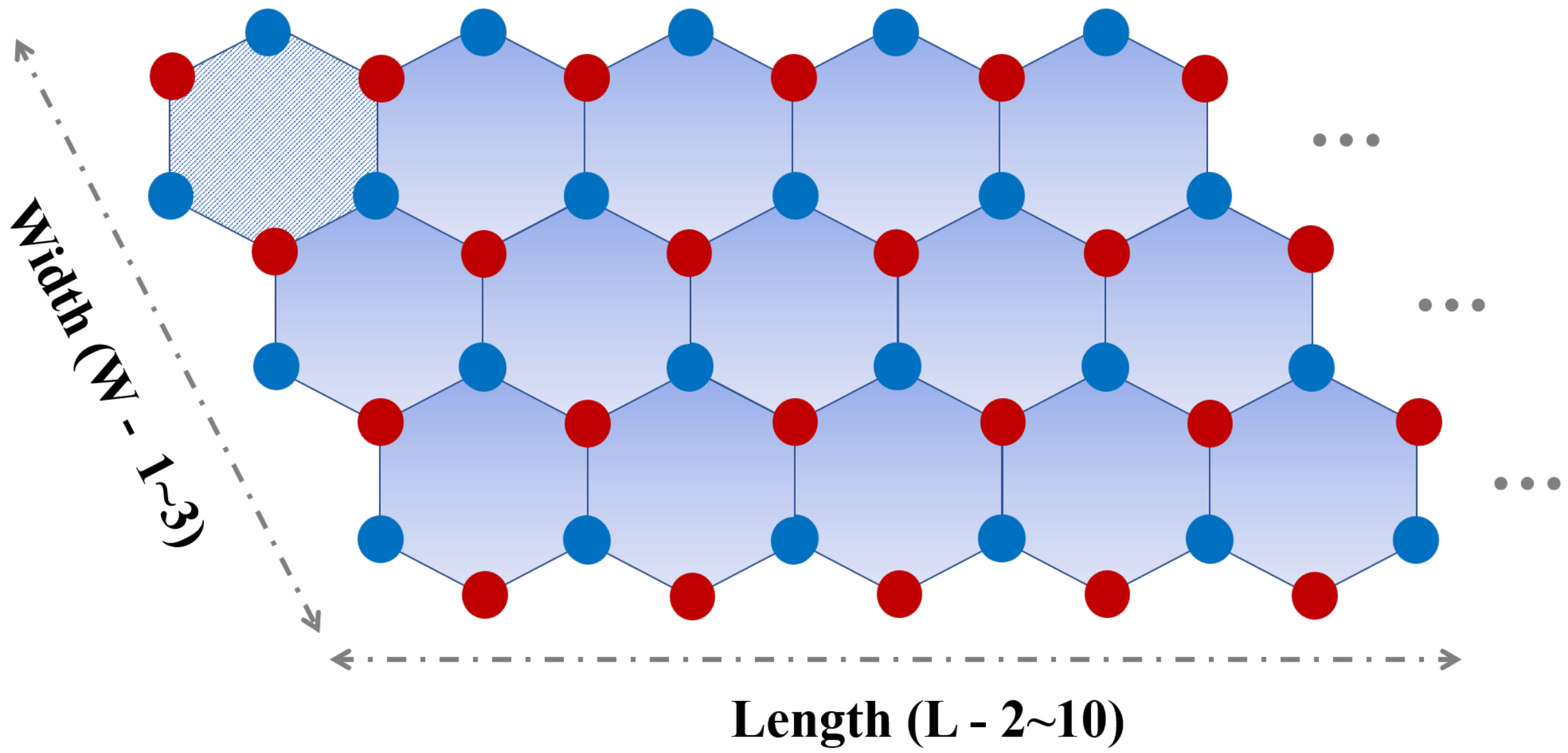
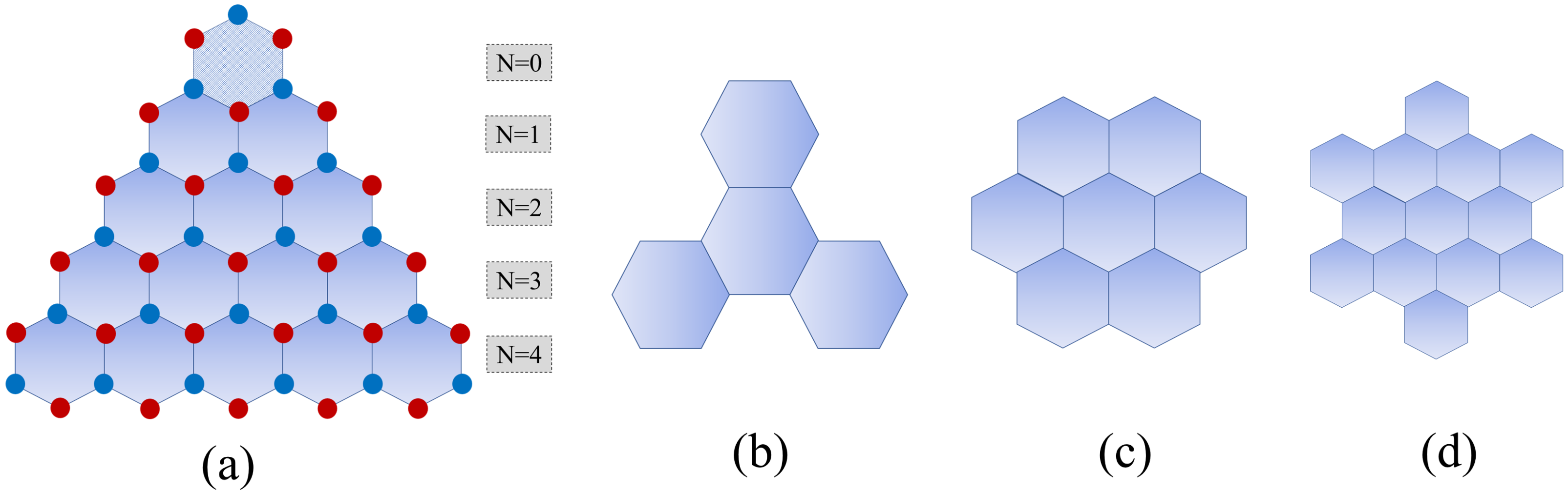
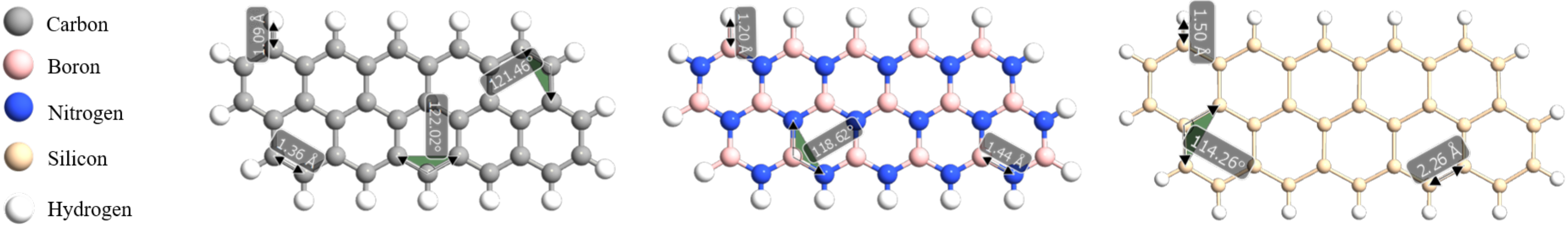
2.1. Model
2.2. Computational Details
3. Electronic Properties
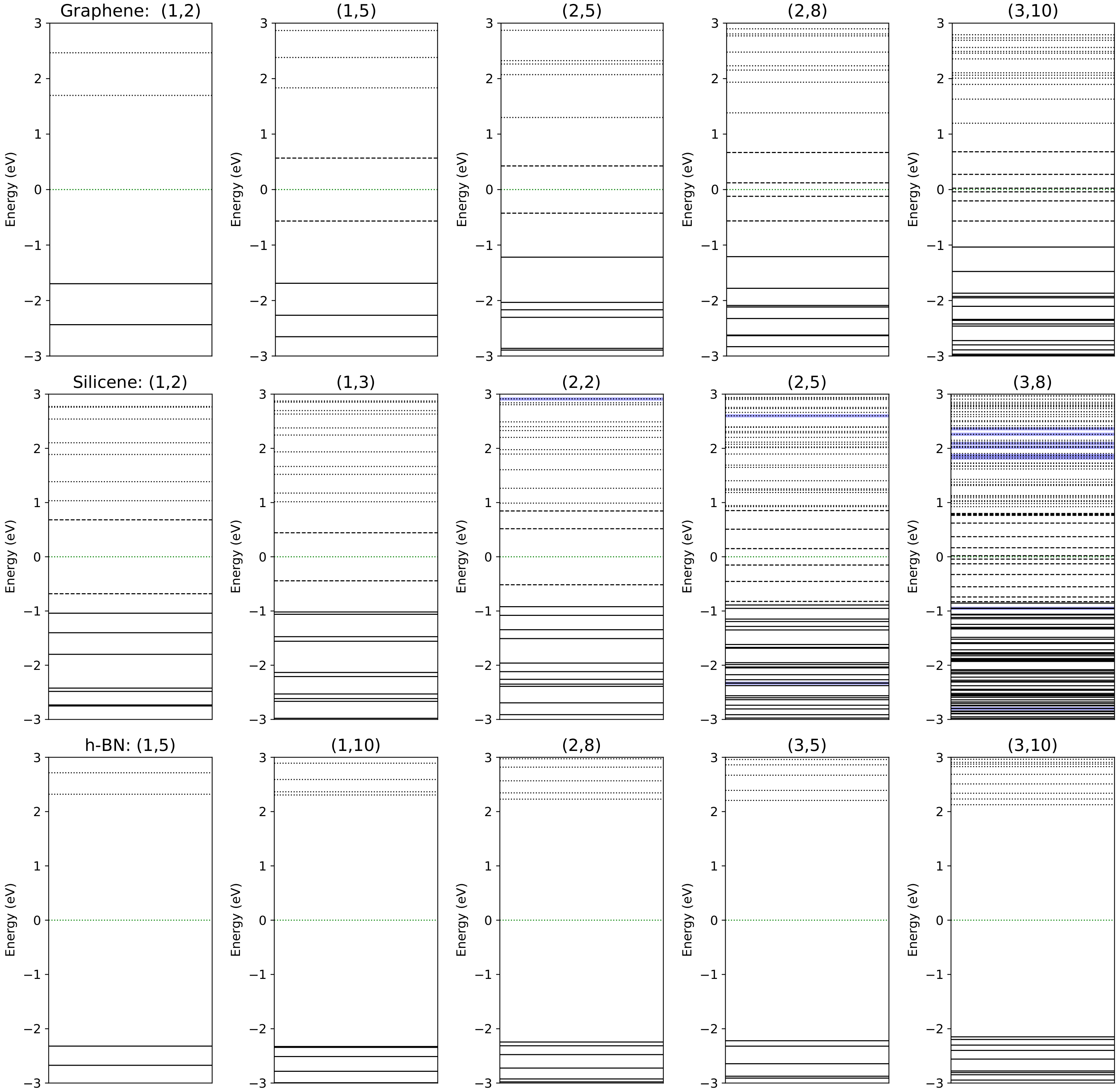
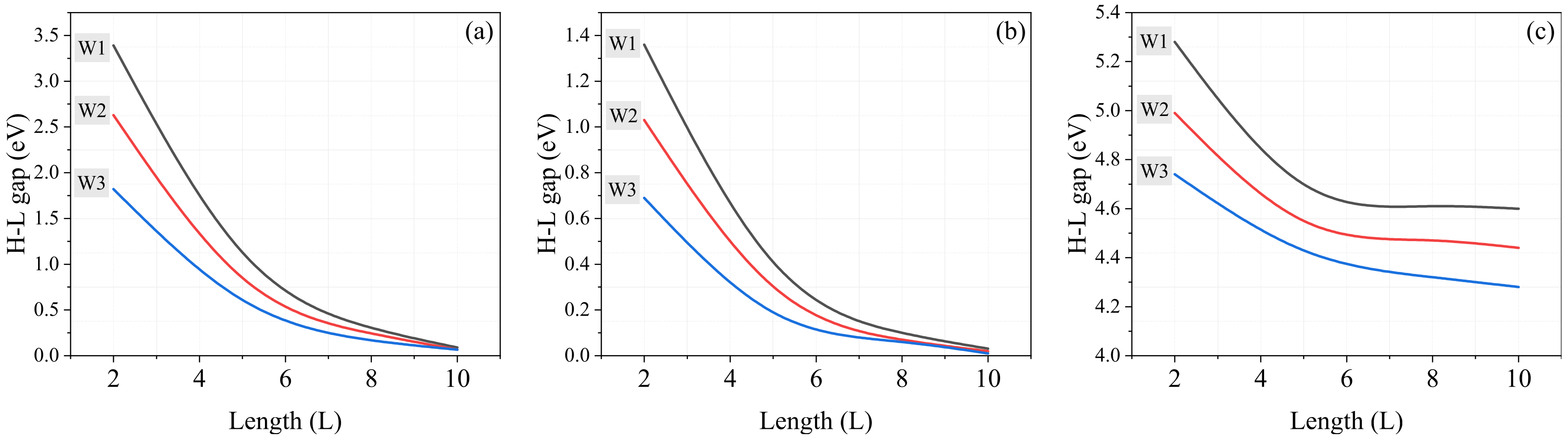
3.1. Finite-Length Nanoribbons
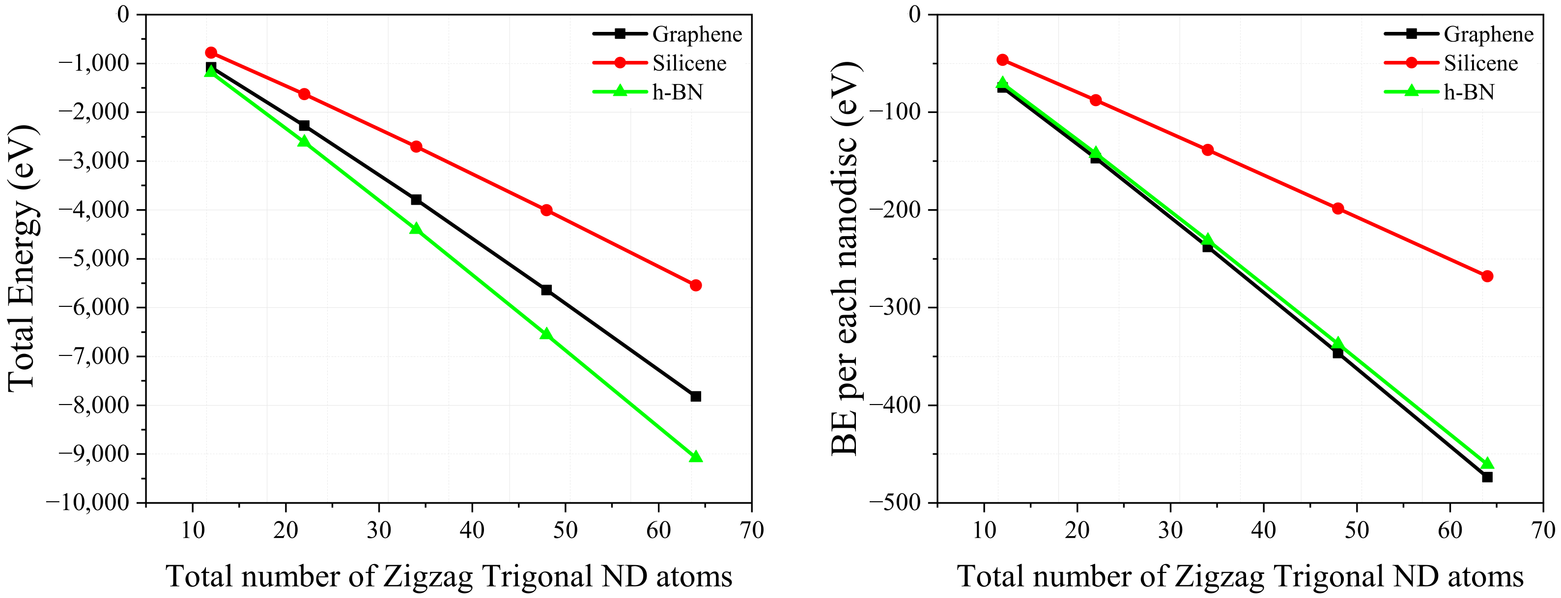
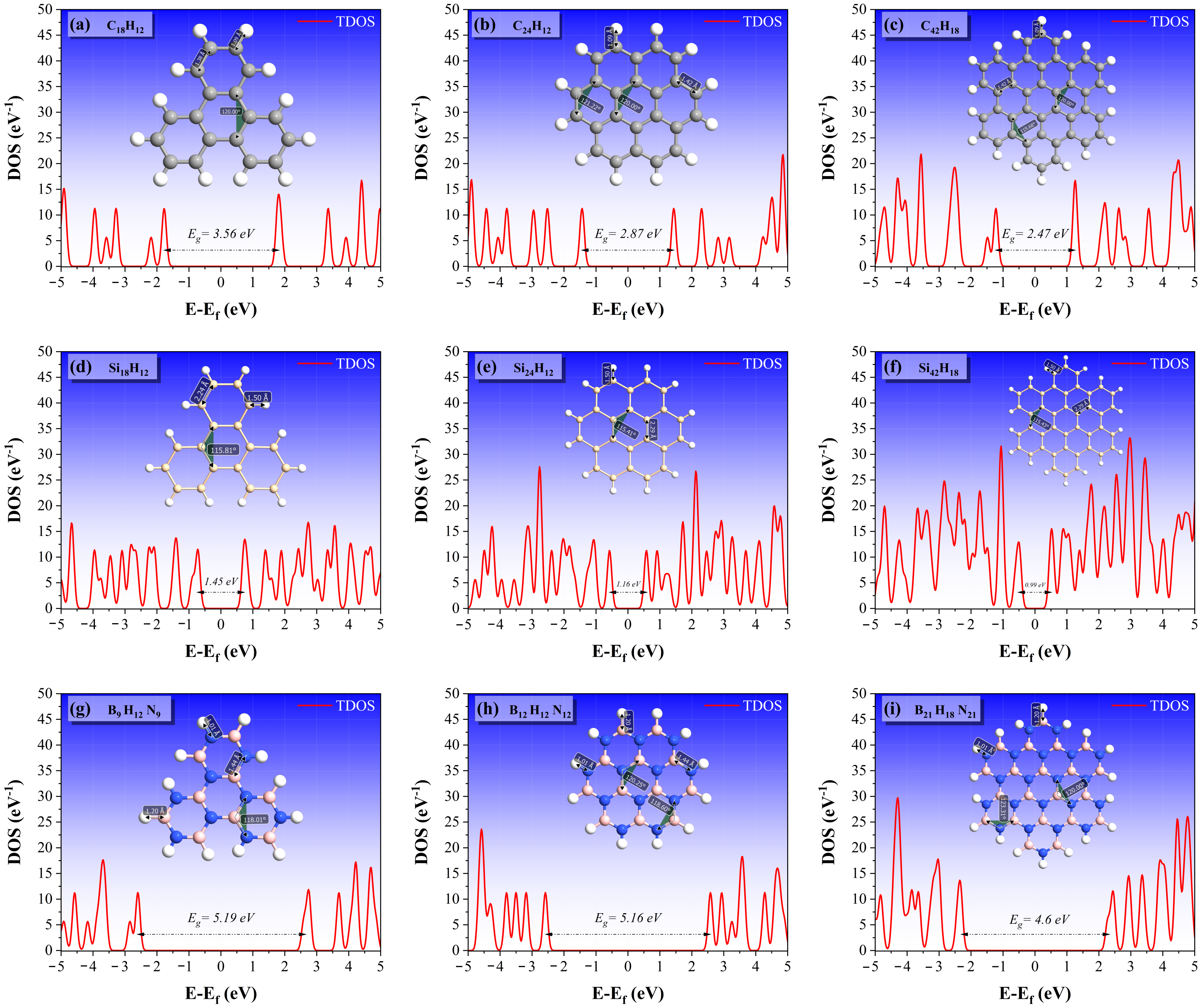
3.2. Nanodiscs
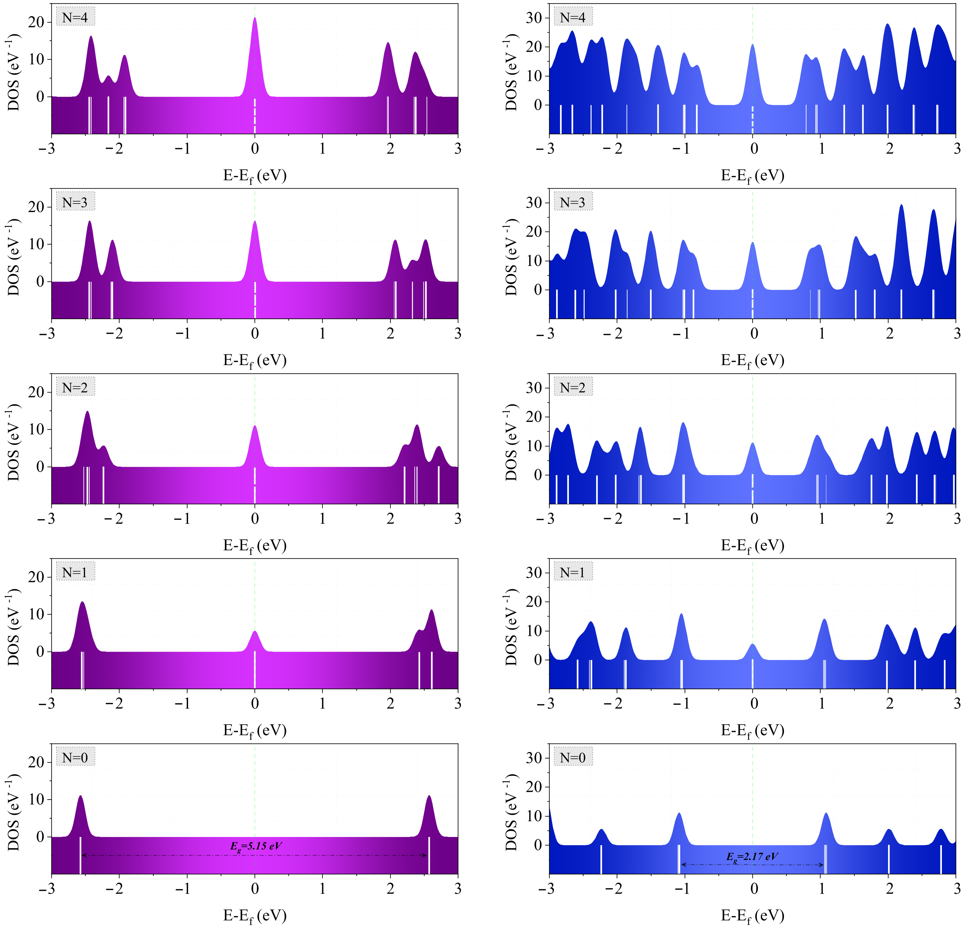
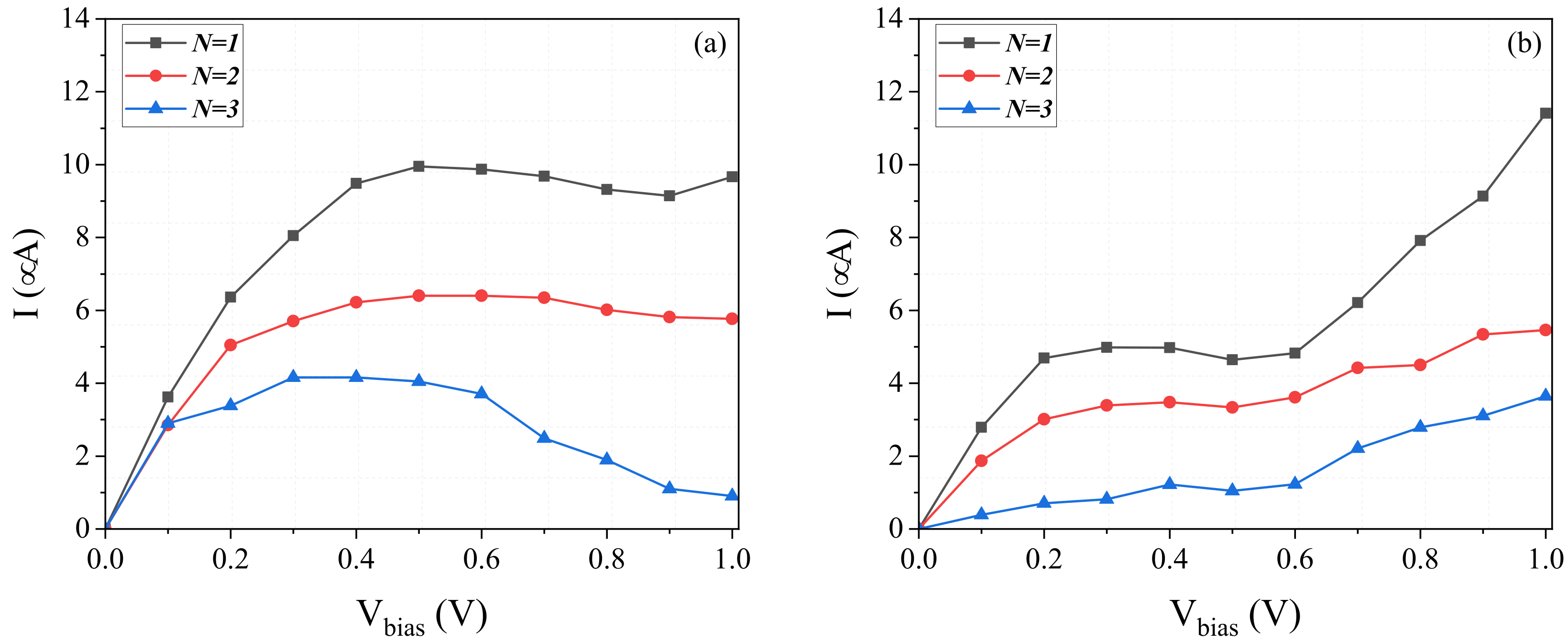
4. Transport Properties
5. Conclusions
Supplementary Materials
Author Contributions
Funding
Institutional Review Board Statement
Informed Consent Statement
Data Availability Statement
Acknowledgments
Conflicts of Interest
References
- Novoselov, K.S.; Geim, A.K.; Morozov, S.V.; Jiang, D.E.; Zhang, Y.; Dubonos, S.V.; Grigorieva, I.V.; Firsov, A.A. Electric field effect in atomically thin carbon films. Science 2004, 306, 666–669. [Google Scholar] [CrossRef] [PubMed] [Green Version]
- Novoselov, K.S.; Geim, A.K.; Morozov, S.V.; Jiang, D.; Katsnelson, M.I.; Grigorieva, I.; Dubonos, S.; Firsov., A.A. Two-dimensional gas of massless Dirac fermions in graphene. Nature 2005, 438, 197–200. [Google Scholar] [CrossRef] [PubMed]
- Zhang, Y.; Tan, Y.W.; Stormer, H.L.; Kim, P. Experimental observation of the quantum Hall effect and Berry’s phase in graphene. Nature 2005, 438, 201–204. [Google Scholar] [CrossRef] [PubMed] [Green Version]
- Rycerz, A.; Tworzydło, J.; Beenakker, C.W.J. Valley filter and valley valve in graphene. Nat. Phys. 2007, 3, 172–175. [Google Scholar] [CrossRef] [Green Version]
- Geim, A.K.; Novoselov, K.S. The rise of graphene. In Nanoscience and Technology: A Collection of Reviews from Nature Journals; World Scientific: Singapore, 2010; pp. 11–19. [Google Scholar]
- Neto, A.H.C.; Guinea, F.; Peres, N.M.R.; Novoselov, K.S.; Geim, A.K. The electronic properties of graphene. Rev. Mod. Phys. 2009, 81, 109. [Google Scholar]
- Novoselov, K.S.; Jiang, Z.; Zhang, Y.; Morozov, S.V.; Stormer, H.L.; Zeitler, U.; Maan, J.C.; Boebinger, G.S.; Kim, P.; Geim, A.K. Room-temperature quantum Hall effect in graphene. Science 2007, 315, 1379. [Google Scholar] [CrossRef] [Green Version]
- Jiang, Z.; Zhang, Y.; Tan, Y.W.; Stormer, H.L.; Kim, P. Quantum Hall effect in graphene. Solid State Commun. 2007, 143, 14–19. [Google Scholar] [CrossRef]
- Liao, L.; Lin, Y.C.; Bao, M.; Cheng, R.; Bai, J.; Liu, Y.; Qu, Y.; Wang, K.L.; Huang, Y.; Duan, X. High-speed graphene transistors with a self-aligned nanowire gate. Nature 2010, 467, 305–308. [Google Scholar] [CrossRef]
- Nakada, K.; Fujita, M.; Dresselhaus, G.; Dresselhaus, M.S. Edge state in graphene ribbons: Nanometer size effect and edge shape dependence. Phys. Rev. B 1996, 54, 17954. [Google Scholar] [CrossRef] [Green Version]
- Wakabayashi, K.; Fujita, M.; Ajiki, H.; Sigrist, M. Electronic and magnetic properties of nanographite ribbons. Phys. Rev. B 1999, 59, 8271. [Google Scholar] [CrossRef] [Green Version]
- Wassmann, T.; Seitsonen, A.P.; Saitta, A.M.; Lazzeri, M.; Mauri, F. Structure, stability, edge states, and aromaticity of graphene ribbons. Phys. Rev. Lett. 2008, 101, 96402. [Google Scholar] [CrossRef] [PubMed] [Green Version]
- Yang, L.; Cohen, M.L.; Louie, S.G. Magnetic edge-state excitons in zigzag graphene nanoribbons. Phys. Rev. Lett. 2008, 101, 186401. [Google Scholar] [CrossRef] [PubMed]
- Cai, J.; Ruffieux, P.; Jaafar, R.; Bieri, M.; Braun, T.; Blankenburg, S.; Muoth, M.; Seitsonen, A.P.; Saleh, M.; Feng, X.; et al. Atomically precise bottom-up fabrication of graphene nanoribbons. Nature 2010, 466, 470–473. [Google Scholar] [CrossRef] [PubMed]
- Berger, C.; Song, Z.; Li, X.; Wu, X.; Brown, N.; Naud, C.; Mayou, D.; Li, T.; Hass, J.; Marchenkov, A.N.; et al. Electronic confinement and coherence in patterned epitaxial graphene. Science 2006, 312, 1191–1196. [Google Scholar] [CrossRef] [Green Version]
- Chen, Z.; Lin, Y.M.; Rooks, M.J.; Avouris, P. Graphene nano-ribbon electronics. Phys. E Low-Dimens. Syst. Nanostruct. 2007, 40, 228–232. [Google Scholar] [CrossRef]
- Han, M.Y.; Özyilmaz, B.; Zhang, Y.; Kim, P. Energy band-gap engineering of graphene nanoribbons. Phys. Rev. Lett. 2007, 98, 206805. [Google Scholar] [CrossRef] [Green Version]
- Fujita, M.; Wakabayashi, K.; Nakada, K.; Kusakabe, K. Peculiar localized state at zigzag graphite edge. J. Phys. Soc. Jpn. 1996, 65, 1920–1923. [Google Scholar] [CrossRef] [Green Version]
- Ezawa, M. Peculiar width dependence of the electronic properties of carbon nanoribbons. Phys. Rev. B 2006, 73, 45432. [Google Scholar] [CrossRef] [Green Version]
- Hod, O.; Barone, V.; Peralta, J.E.; Scuseria, G.E. Enhanced half-metallicity in edge-oxidized zigzag graphene nanoribbons. Nano Lett. 2007, 7, 2295–2299. [Google Scholar] [CrossRef] [Green Version]
- Räder, H.J.; Rouhanipour, A.; Talarico, A.M.; Palermo, V.; Samorì, P.; Müllen, K. Processing of giant graphene molecules by soft-landing mass spectrometry. Nat. Mater. 2006, 5, 276–280. [Google Scholar] [CrossRef]
- Sheardy, A.T.; Arvapalli, D.M.; Wei, J. Novel microwave synthesis of near-metallic copper sulfide nanodiscs with size control: Experimental and DFT studies of charge carrier density. Nanoscale Adv. 2020, 2, 1054–1058. [Google Scholar] [CrossRef] [Green Version]
- Yamamoto, T.; Noguchi, T.; Watanabe, K. Edge-state signature in optical absorption of nanographenes: Tight-binding method and time-dependent density functional theory calculations. Phys. Rev. B 2006, 74, 121409. [Google Scholar] [CrossRef] [Green Version]
- Ezawa, M. Peculiar band gap structure of graphene nanoribbons. Phys. Status Solidi C 2007, 4, 489–492. [Google Scholar] [CrossRef] [Green Version]
- Denisov, I.G.; Sligar, S.G. Nanodiscs for structural and functional studies of membrane proteins. Nat. Struct. Mol. Biol. 2016, 23, 481–486. [Google Scholar] [CrossRef] [PubMed]
- Jin, C.; Lin, F.; Suenaga, K.; Iijima, S. Fabrication of a freestanding boron nitride single layer and its defect assignments. Phys. Rev. Lett. 2009, 102, 195505. [Google Scholar] [CrossRef] [Green Version]
- Ramakrishna Matte, H.S.S.; Gomathi, A.; Manna, A.K.; Late, D.J.; Datta, R.; Pati, S.K.; Rao, C.N.R. MoS2 and WS2 analogues of graphene. Angew. Chem. Int. Ed. 2010, 49, 4059–4062. [Google Scholar] [CrossRef]
- Kaasbjerg, K.; Thygesen, K.S.; Jacobsen, K.W. Phonon-limited mobility in n-type single-layer MoS 2 from first principles. Phys. Rev. B 2012, 85, 115317. [Google Scholar] [CrossRef] [Green Version]
- Vogt, P.; De Padova, P.; Quaresima, C.; Avila, J.; Frantzeskakis, E.; Asensio, M.C.; Resta, A.; Ealet, B.; Le Lay, G. Silicene: Compelling experimental evidence for graphenelike two-dimensional silicon. Phys. Rev. Lett. 2012, 108, 155501. [Google Scholar] [CrossRef]
- Butler, S.Z.; Hollen, S.M.; Cao, L.; Cui, Y.; Gupta, J.A.; Gutiérrez, H.R.; Heinz, T.F.; Hong, S.S.; Huang, J.; Ismach, A.F.; et al. Progress, challenges, and opportunities in two-dimensional materials beyond graphene. ACS Nano 2013, 7, 2898–2926. [Google Scholar] [CrossRef]
- Jafari, M.; Wawrzyniak-Adamczewska, M.; Stagraczyński, S.; Dyrdal, A.; Barnaś, J. Spin valve effect in two-dimensional VSe2 294 system. J. Magn. Magn. Mater. 2022, 548, 168921. [Google Scholar] [CrossRef]
- Song, X.; Hu, J.; Zeng, H. Two-dimensional semiconductors: Recent progress and future perspectives. J. Mater. Chem. C 2013, 1, 2952–2969. [Google Scholar] [CrossRef]
- Xu, M.; Liang, T.; Shi, M.; Chen, H. Graphene-like two-dimensional materials. Chem. Rev. 2013, 113, 3766–3798. [Google Scholar] [CrossRef] [PubMed]
- Tang, Q.; Zhou, Z.; Chen, Z. Innovation and discovery of graphene-like materials via density-functional theory computations. Wiley Interdiscip. Rev. Comput. Mol. Sci. 2015, 5, 360–379. [Google Scholar] [CrossRef]
- Jafari, M.A.; Kordbacheh, A.A.; Mahdian, S.; Ghasemi, N. Electronic and transport properties of (6, 2) carbon and silicon nanotubes: A first-principles calculation. Phys. E Low-Dimens. Syst. Nanostruct. 2020, 117, 113855. [Google Scholar] [CrossRef]
- Gupta, A.; Sakthivel, T.; Seal, S. Recent development in 2D materials beyond graphene. Prog. Mater. Sci. 2015, 73, 44–126. [Google Scholar] [CrossRef]
- Fattahi, A.M.; Safaei, B.; Ahmed, N.A. A comparison for the non-classical plate model based on axial buckling of single-layered graphene sheets. Springer Berl. Heidelb. 2019, 134, 555. [Google Scholar] [CrossRef]
- Babak, S.; Hamed, K.F.; Fattahi, A.M. Non-classical plate model for single-layered graphene sheet for axial buckling. Adv. Nano Res. 2019, 7, 265–275. [Google Scholar]
- Zhang, J.J.; Lin, L.; Zhang, Y.; Wu, M.; Yakobson, B.I.; Dong, S. Type-II multiferroic Hf2VC2F2 MXene monolayer with high transition temperature. J. Am. Chem. Soc. 2018, 140, 9768–9773. [Google Scholar] [CrossRef] [Green Version]
- Liu, W.; Luo, X.; Bao, Y.; Liu, Y.P.; Ning, G.H.; Abdelwahab, I.; Li, L.; Nai, C.T.; Hu, Z.G.; Zhao, D.; et al. A two-dimensional conjugated aromatic polymer via C–C coupling reaction. Nat. Chem. 2017, 9, 563–570. [Google Scholar] [CrossRef]
- Wang, R.; Purdie, D.G.; Fan, Y.; Massabuau, F.C.P.; Braeuninger-Weimer, P.; Burton, O.J.; Blume, R.; Schloegl, R.; Lombardo, A.; Weatherup, R.S.; et al. A peeling approach for integrated manufacturing of large monolayer h-BN crystals. ACS Nano 2019, 13, 2114–2126. [Google Scholar] [CrossRef] [Green Version]
- Whelan, P.R.; Jessen, B.S.; Wang, R.; Luo, B.; Stoot, A.C.; Mackenzie, D.M.A.; Braeuninger-Weimer, P.; Jouvray, A.; Prager, L.; Camilli, L.; et al. Raman spectral indicators of catalyst decoupling for transfer of CVD grown 2D materials. Carbon 2017, 117, 75–81. [Google Scholar] [CrossRef] [Green Version]
- Liu, J.; Yang, Y.; Lyu, P.; Nachtigall, P.; Xu, Y. Few-layer silicene nanosheets with superior lithium-storage properties. Adv. Mater. 2018, 30, 1800838. [Google Scholar] [CrossRef] [PubMed]
- Feng, B.; Ding, Z.; Meng, S.; Yao, Y.; He, X.; Cheng, P.; Chen, L.; Wu, K. Evidence of silicene in honeycomb structures of silicon on Ag (111). Nano Lett. 2012, 12, 3507–3511. [Google Scholar] [CrossRef] [PubMed] [Green Version]
- Peng, J.; Wu, J.; Li, X.; Zhou, Y.; Yu, Z.; Guo, Y.; Wu, J.; Lin, Y.; Li, Z.; Wu, X.; et al. Very large-sized transition metal dichalcogenides monolayers from fast exfoliation by manual shaking. J. Am. Chem. Soc. 2017, 139, 9019–9025. [Google Scholar] [CrossRef]
- Ezawa, M. Metallic graphene nanodisks: Electronic and magnetic properties. Phys. Rev. B 2007, 76, 245415. [Google Scholar] [CrossRef] [Green Version]
- Ezawa, M. Graphene nanoribbon and graphene nanodisk. Phys. E Low-Dimens. Syst. Nanostruct. 2008, 40, 1421–1423. [Google Scholar] [CrossRef] [Green Version]
- Ezawa, M. Coulomb blockade in graphene nanodisks. Phys. Rev. B 2008, 77, 155411. [Google Scholar] [CrossRef] [Green Version]
- Ezawa, M. Quasi-ferromagnet spintronics in the graphene nanodisc–lead system. New J. Phys. 2009, 11, 95005. [Google Scholar] [CrossRef]
- Ezawa, M. Spin filter, spin amplifier and spin diode in graphene nanodisk. Eur. Phys. J. B 2009, 67, 543–549. [Google Scholar] [CrossRef]
- Maruyama, M.; Okada, S. Energetics and electronic structure of triangular hexagonal boron nitride nanoflakes. Sci. Rep. 2018, 8, 1–10. [Google Scholar] [CrossRef]
- Yamanaka, A.; Okada, S. Energetics and electronic structure of h-BN nanoflakes. Sci. Rep. 2016, 6, 1–9. [Google Scholar] [CrossRef] [PubMed] [Green Version]
- Kohn, W.; Sham, L.J. Self-consistent equations including exchange and correlation effects. Phys. Rev. 1965, 140, A1133. [Google Scholar] [CrossRef] [Green Version]
- van Setten, M.J.; Giantomassi, M.; Bousquet, E.; Verstraete, M.J.; Hamann, D.R.; Gonze, X.; Rignanese, G.M. The PseudoDojo: Training and grading a 85 element optimized norm-conserving pseudopotential table. Comput. Phys. Commun. 2018, 226, 39–54. [Google Scholar] [CrossRef] [Green Version]
- Smidstrup, S.; Stradi, D.; Wellendorff, J.; Khomyakov, P.A.; Vej-Hansen, U.G.; Lee, M.E.; Ghosh, T.; Jónsson, E.; Jónsson, H.; Stokbro, K. First-principles Green’s-function method for surface calculations: A pseudopotential localized basis set approach. Phys. Rev. B 2017, 96, 195309. [Google Scholar] [CrossRef] [Green Version]
- Smidstrup, S.; Markussen, T.; Vancraeyveld, P.; Wellendorff, J.; Schneider, J.; Gunst, T.; Verstichel, B.; Stradi, D.; Khomyakov, P.A.; Vej-Hansen, U.G.; et al. QuantumATK: An integrated platform of electronic and atomic-scale modelling tools. J. Phys. Condens. Matter 2019, 32, 15901. [Google Scholar] [CrossRef]
- Perdew, J.P.; Burke, K.; Ernzerhof, M. Generalized gradient approximation made simple. Phys. Rev. Lett. 1996, 77, 3865. [Google Scholar] [CrossRef] [Green Version]
- Monkhorst, H.J.; Pack, J.D. Special points for Brillouin-zone integrations. Phys. Rev. B 1976, 13, 5188. [Google Scholar] [CrossRef]
- Mads, B.; José-Luis, M.; Pablo, O.; Kurt, T.J.A.S. Density-functional method for nonequilibrium electron transport. Phys. Rev. B 2002, 65, 165401. [Google Scholar]
- Stradi, D.; Martinez, U.; Blom, A.; Brandbyge, M.; Stokbro, K. General atomistic approach for modeling metal-semiconductor interfaces using density functional theory and nonequilibrium Green’s function. Phys. Rev. B 2016, 93, 155302. [Google Scholar] [CrossRef] [Green Version]
- Lopez-Bezanilla, A.; Huang, J.; Terrones, H.; Sumpter, B.G. Boron nitride nanoribbons become metallic. Nano Lett. 2011, 11, 3267–3273. [Google Scholar] [CrossRef]
- Shi, Y.; Hamsen, C.; Jia, X.; Kim, K.K.; Reina, A.; Hofmann, M.; Hsu, A.L.; Zhang, K.; Li, H.; Juang, Z.Y.; et al. Synthesis of few-layer hexagonal boron nitride thin film by chemical vapor deposition. Nano Lett. 2010, 10, 4134–4139. [Google Scholar] [CrossRef] [PubMed]


| Nanodiscs | Graphene | Silicene | h-BN |
|---|---|---|---|
| Zigzag Trigonal N = 0 | −74.690 | −46.341 | −70.727 |
| Zigzag Trigonal N = 1 | −147.23 | −87.756 | −142.230 |
| Zigzag Trigonal N = 2 | −237.902 | −138.524 | −231.058 |
| Zigzag Trigonal N = 3 | −346.729 | −198.634 | −337.234 |
| Zigzag Trigonal N = 4 | −473.695 | −268.040 | −460.753 |
| Armchair Trigonal | −203.079 | −120.520 | −193.244 |
| Zigzag Hexagonal | −257.614 | −148.402 | −245.214 |
| Armchair Hexagonal | −439.875 | −250.579 | −419.759 |
Publisher’s Note: MDPI stays neutral with regard to jurisdictional claims in published maps and institutional affiliations. |
© 2022 by the authors. Licensee MDPI, Basel, Switzerland. This article is an open access article distributed under the terms and conditions of the Creative Commons Attribution (CC BY) license (https://creativecommons.org/licenses/by/4.0/).
Share and Cite
Jafari, M.; Dyrdał, A. First Principle Study on Electronic and Transport Properties of Finite-Length Nanoribbons and Nanodiscs for Selected Two-Dimensional Materials. Molecules 2022, 27, 2228. https://doi.org/10.3390/molecules27072228
Jafari M, Dyrdał A. First Principle Study on Electronic and Transport Properties of Finite-Length Nanoribbons and Nanodiscs for Selected Two-Dimensional Materials. Molecules. 2022; 27(7):2228. https://doi.org/10.3390/molecules27072228
Chicago/Turabian StyleJafari, Mirali, and Anna Dyrdał. 2022. "First Principle Study on Electronic and Transport Properties of Finite-Length Nanoribbons and Nanodiscs for Selected Two-Dimensional Materials" Molecules 27, no. 7: 2228. https://doi.org/10.3390/molecules27072228
APA StyleJafari, M., & Dyrdał, A. (2022). First Principle Study on Electronic and Transport Properties of Finite-Length Nanoribbons and Nanodiscs for Selected Two-Dimensional Materials. Molecules, 27(7), 2228. https://doi.org/10.3390/molecules27072228