
Electron Paramagnetic Resonance Study of PbSe, PbTe, and PbTe:In Semiconductors Obtained by the Pulsed Laser Deposition Method

 ,
,  ,
,  ,
, 

Abstract
:1. Introduction
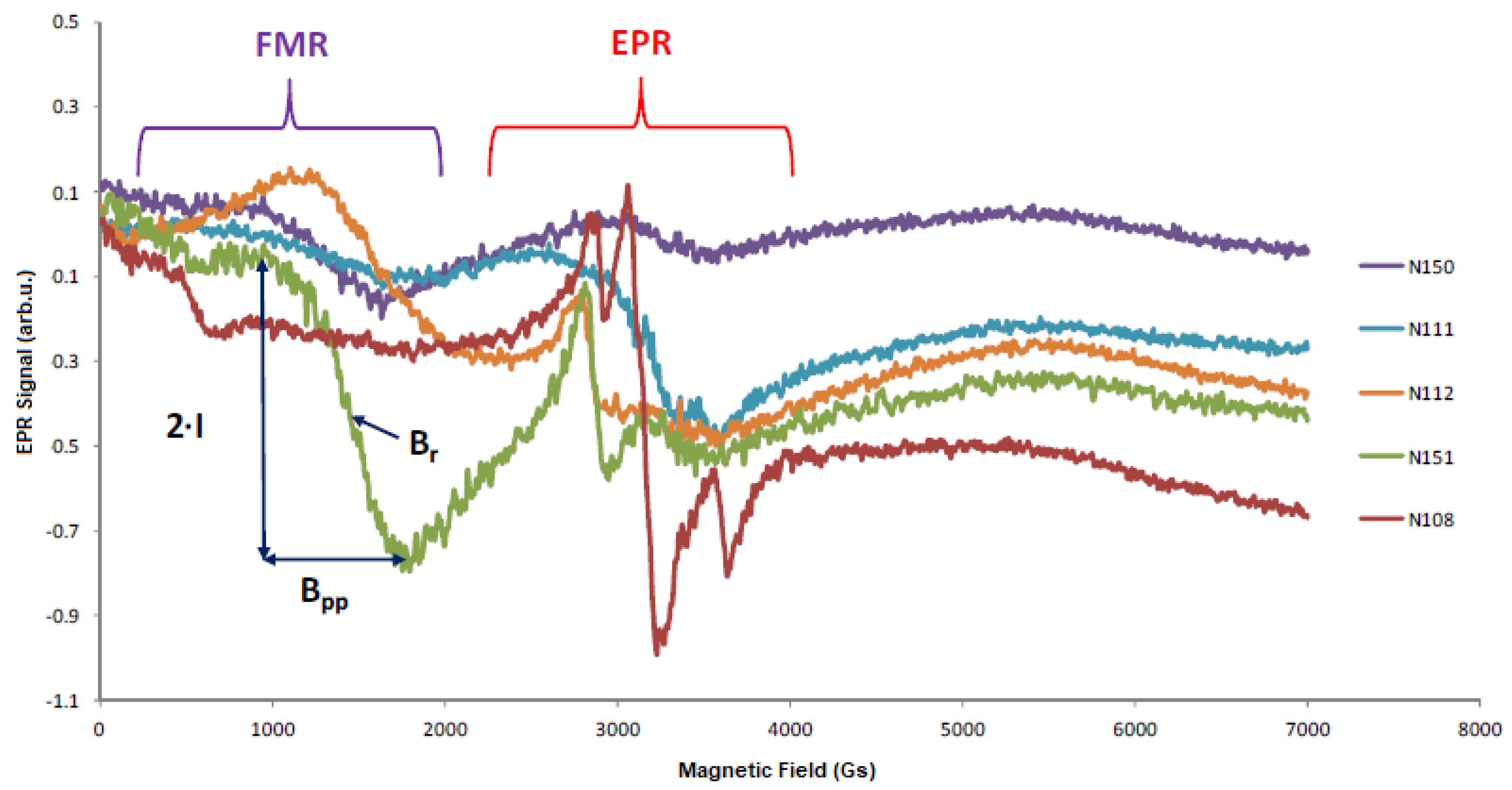
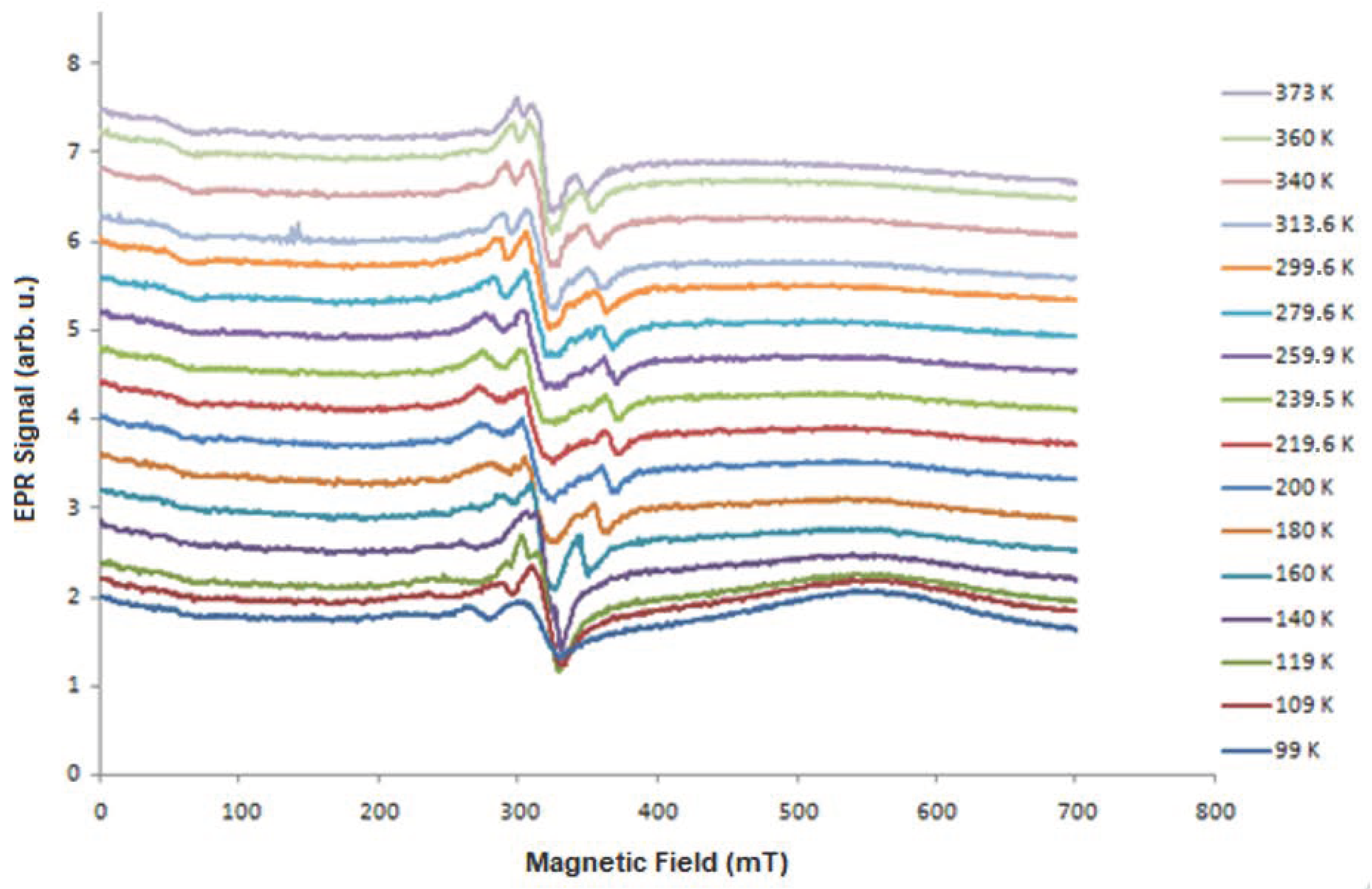
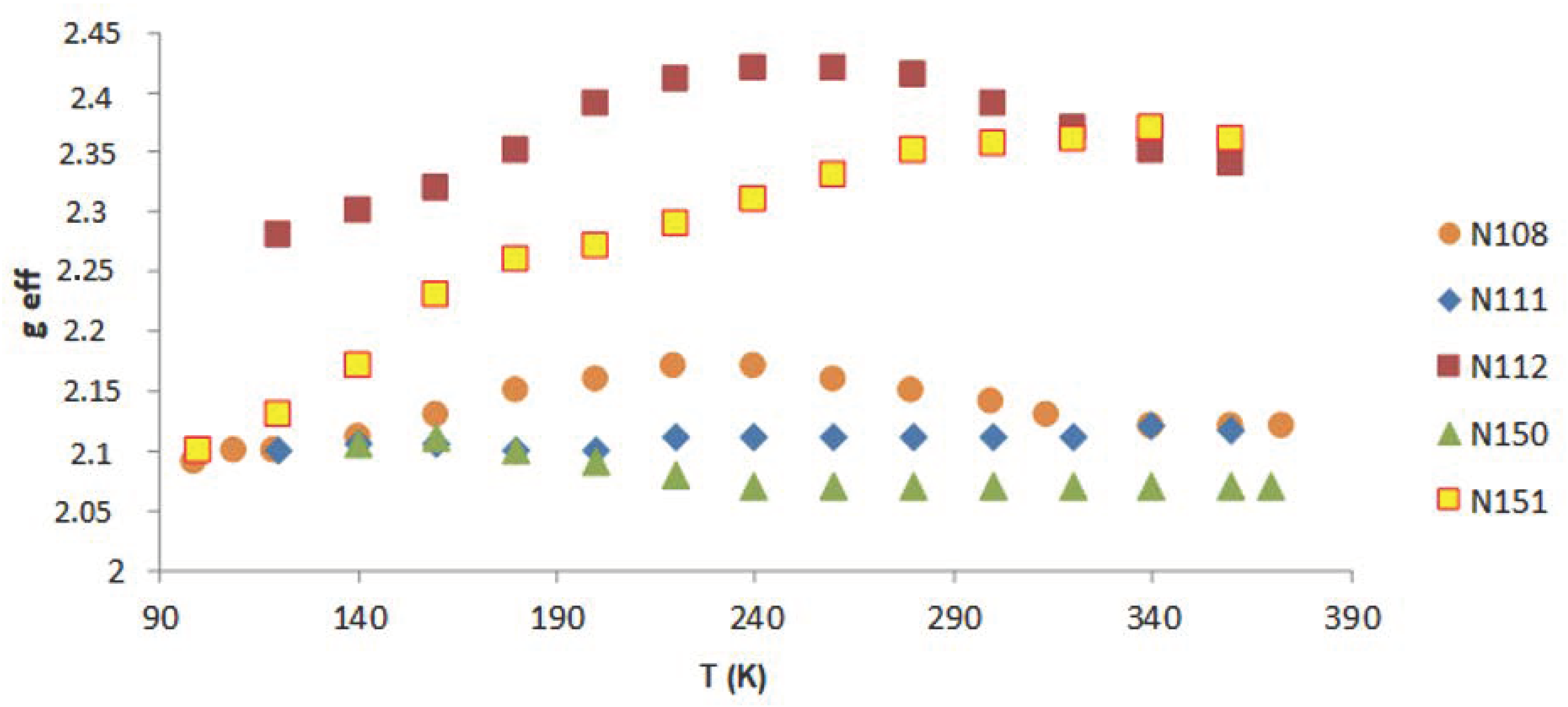
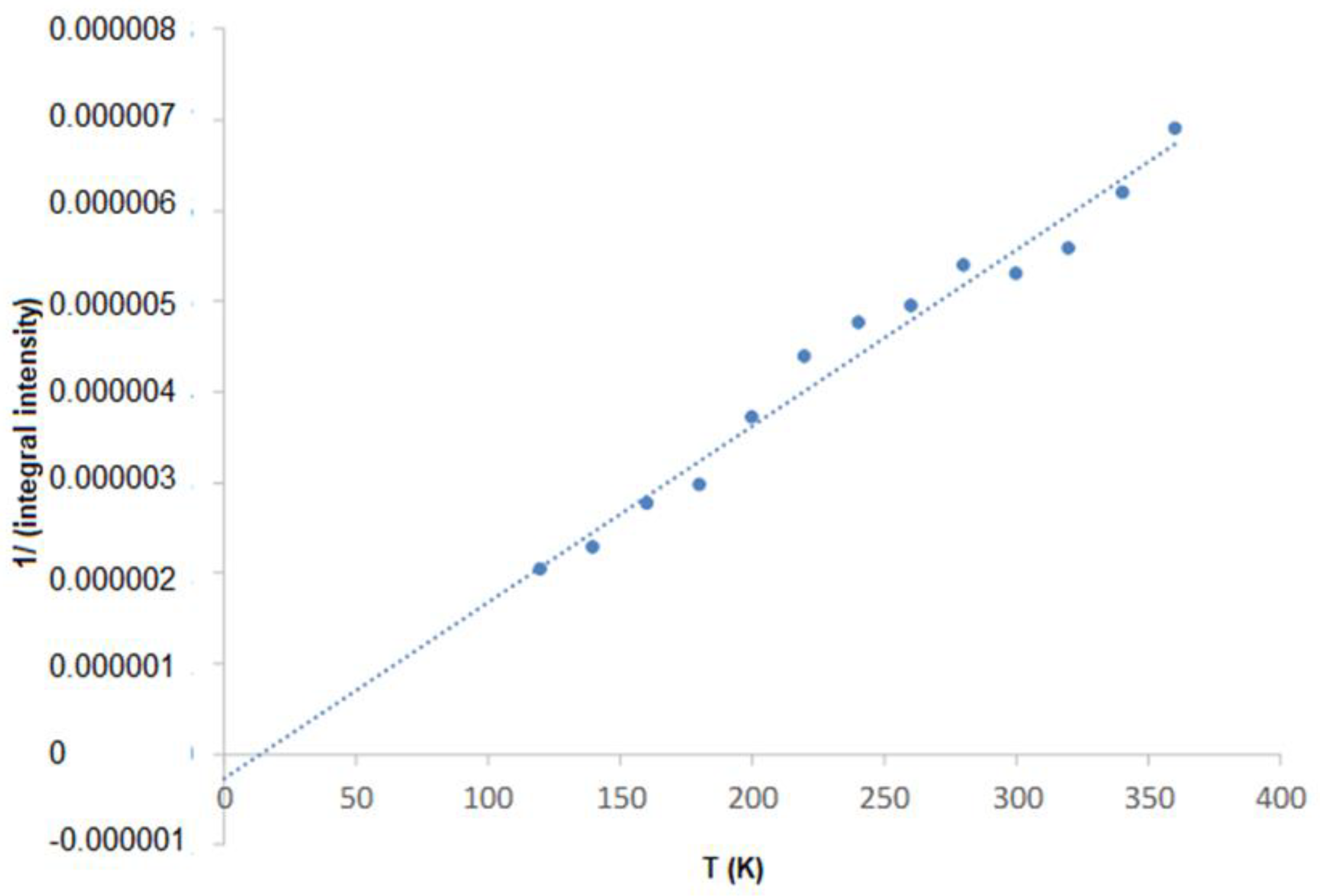
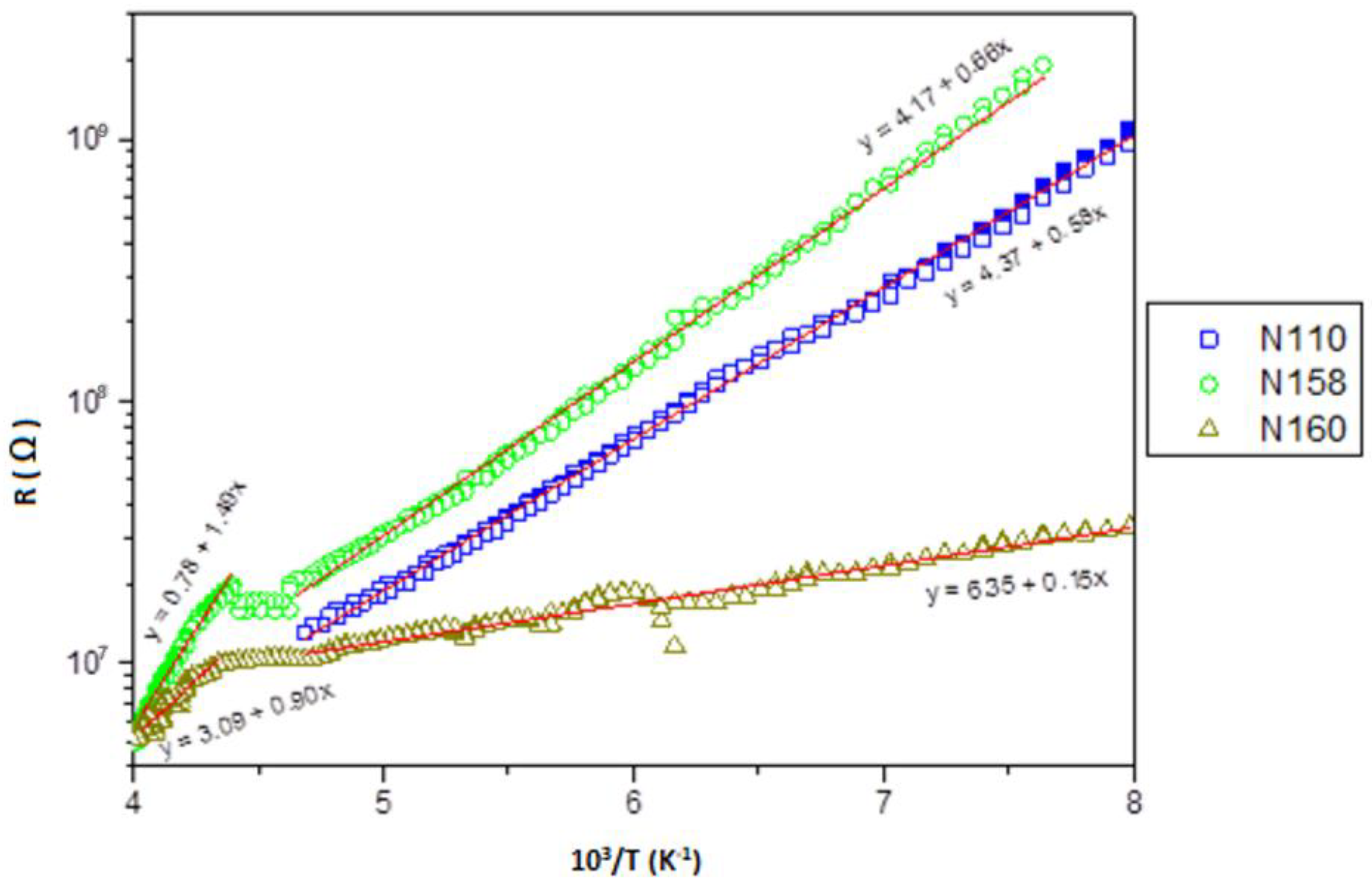
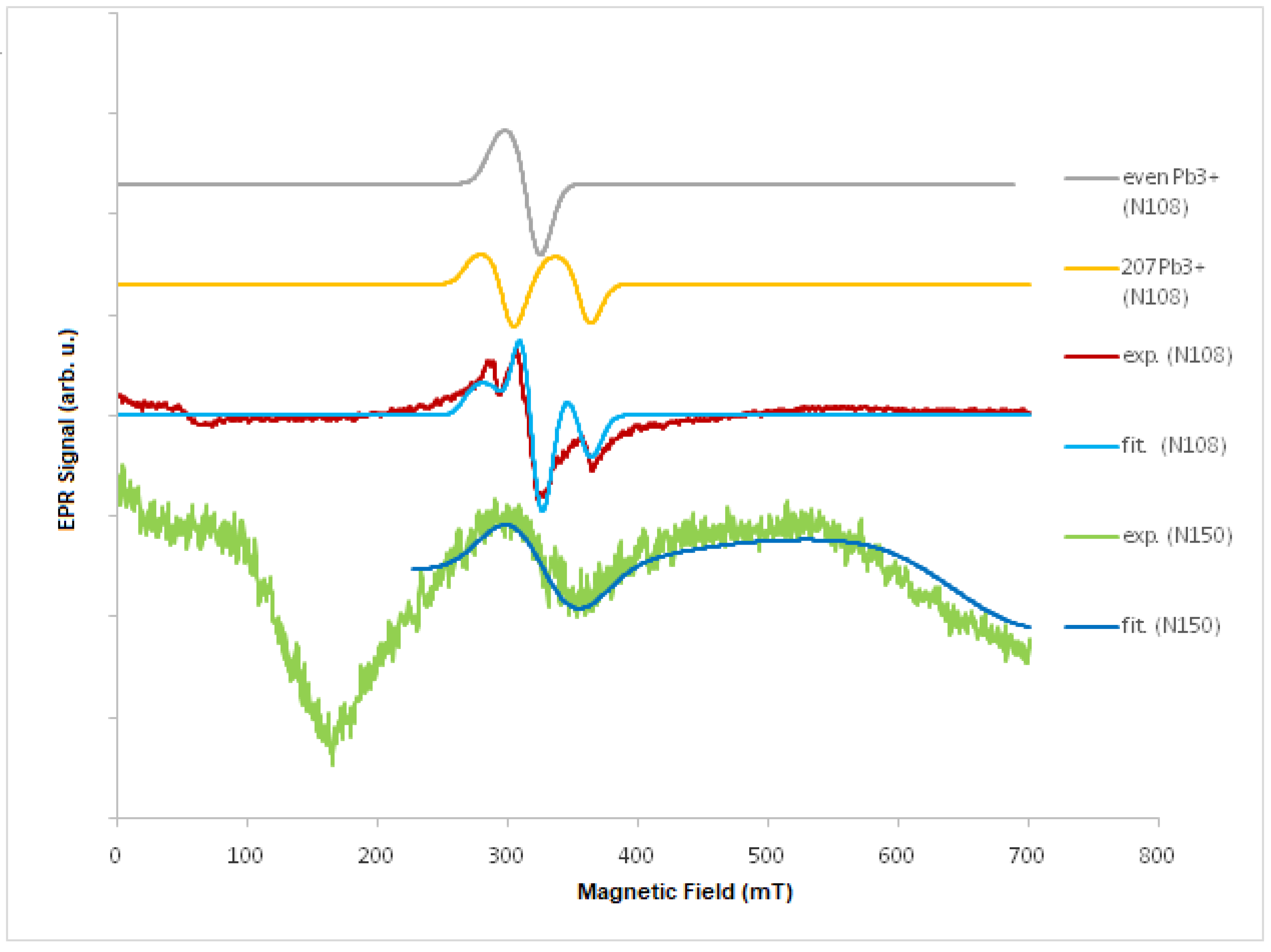
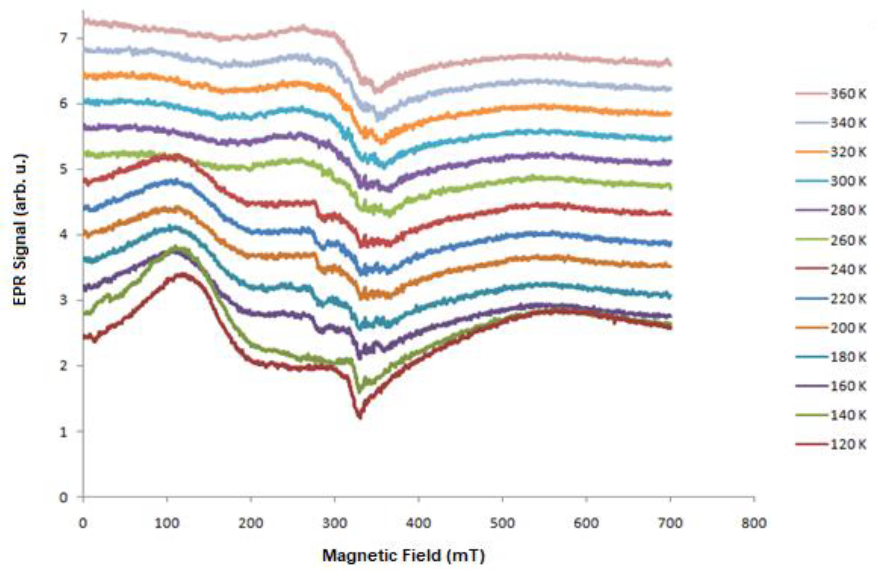
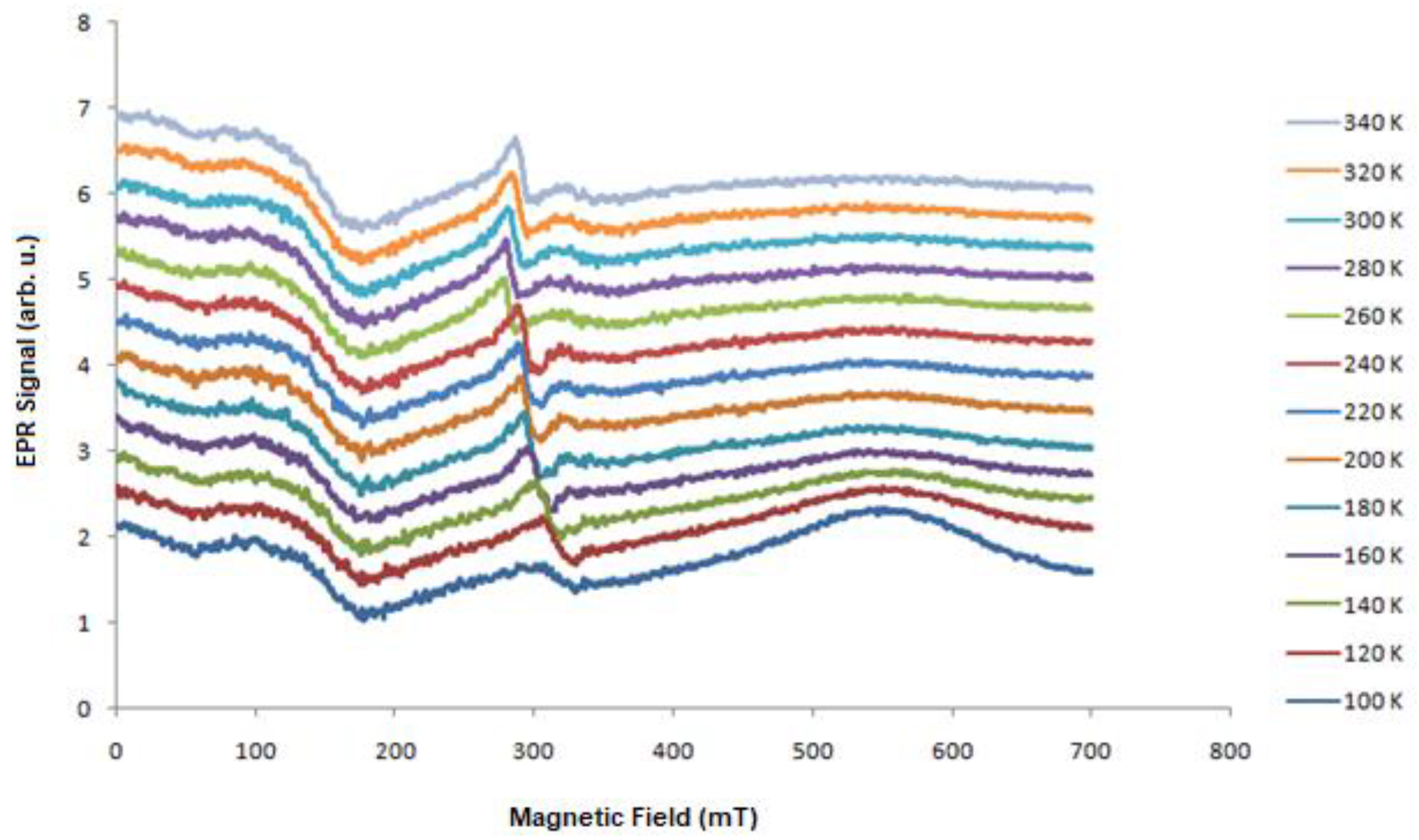
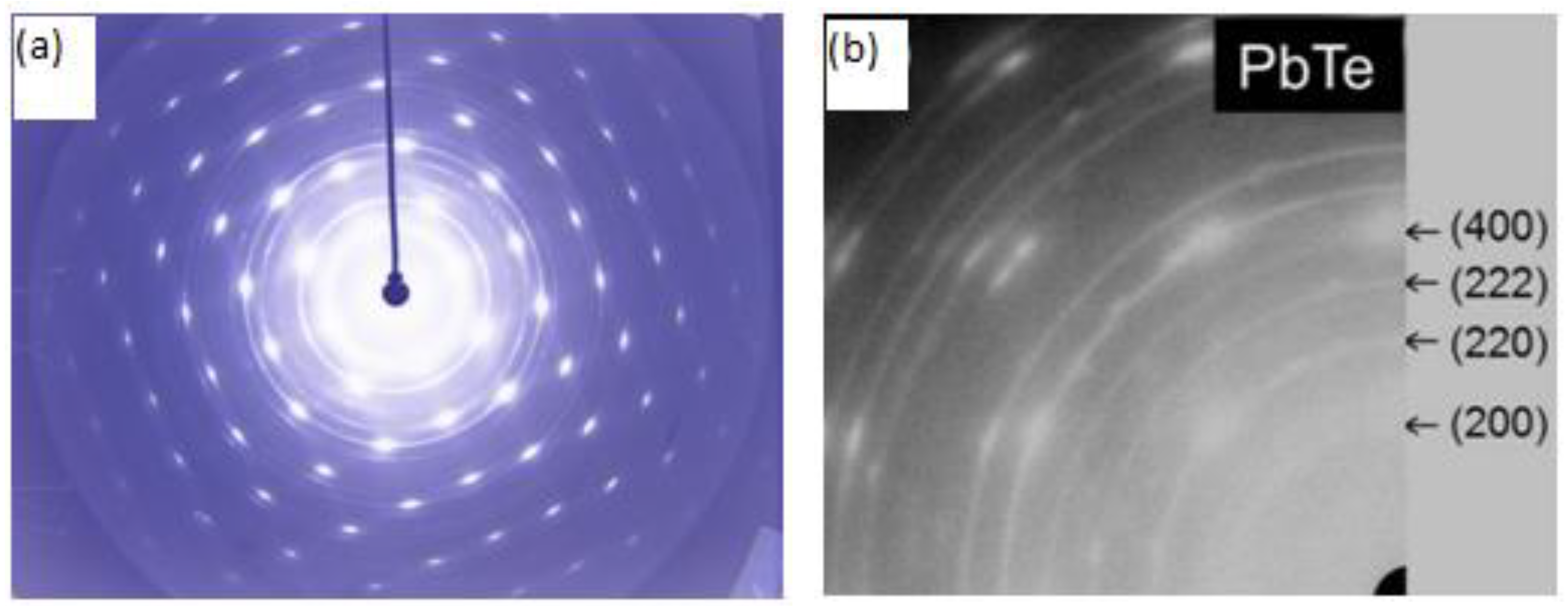
2. Results and Discussion
EPR Measurements
3. Materials and Methods
Electrical Measurements
4. Conclusions
Author Contributions
Funding
Institutional Review Board Statement
Informed Consent Statement
Data Availability Statement
Conflicts of Interest
Sample Availability
References
- Dornhaus, R.; Nimtz, G.; Schlicht, B. Narrow-Gap Semiconductors; Springer: Berlin/Heidelberg, Germany, 1983; Volume 98. [Google Scholar] [CrossRef]
- Bauer, G.; Pascher, H.; Zawadzki, W. Magneto-optical properties of semimagnetic lead chalcogenides. Semicond. Sci. Technol. 1992, 7, 703–723. [Google Scholar] [CrossRef]
- Theocharous, E. Absolute linearity measurements on a PbSe detector in the infrared. Infrared Phys. Technol. 2007, 50, 63–69. [Google Scholar] [CrossRef]
- Isber, S.; Charar, S.; Gratens, X.; Fau, C.; Averous, M. EPR study of the hyperfine structure of ion iSSe, anTe single crystals. Phys. Rev. B Condens. Matter Mater. Phys. 1996, 54, 7634–7636. [Google Scholar] [CrossRef]
- Dietl, T. Origin of ferromagnetic response in diluted magnetic semiconductors and oxides. J. Phys. Condens. Matter 2007, 19, 165204. [Google Scholar] [CrossRef]
- D’Souza, R.; Cao, J.; Querales-Flores, J.D.; Fahy, S.; Savić, I. Electron-phonon scattering and thermoelectric transport in p -type PbTe from first principles. Phys. Rev. B 2020, 102, 115204. [Google Scholar] [CrossRef]
- Lach-Hab, M.; Keegan, M.; Papaconstantopoulos, D.A.; Mehl, M.J. Electronic structure calculations of PbTe. J. Phys. Chem. Solids 2000, 61, 1639–1645. [Google Scholar] [CrossRef]
- Murphy, R.M.; Murray, É.D.; Fahy, S.; Savić, I. Broadband phonon scattering in PbTe-based materials driven near ferroelectric phase transition by strain or alloying. Phys. Rev. B 2016, 93, 104304. [Google Scholar] [CrossRef] [Green Version]
- Dietl, T. Spintronics and ferromagnetism in wide-band-gap semiconductors. AIP Conf. Proc. 2005, 772, 56–64. [Google Scholar]
- Liu, C.; Yun, F.; Morkoç, H. Ferromagnetism of ZnO and GaN: A Review. J. Mater. Sci. Mater. Electron. 2005, 16, 555–597. [Google Scholar] [CrossRef]
- Dietl, T. Origin of ferromagnetism and nano-scale phase separations in diluted magnetic semiconductors. Phys. E Low-Dimens. Syst. Nanostruct. 2006, 35, 293–299. [Google Scholar] [CrossRef]
- Story, T.; Wilamowski, Z.; Grodzicka, E.; Witkowska, B.; Dobrowolski, W. Electron Paramagnetic Resonance of Cr in PbTe. Acta Phys. Pol. A 1993, 84, 773–775. [Google Scholar] [CrossRef]
- Łazarczyk, P.; Story, T.; Arciszewska, M.; Gałęzka, R.R. Magnetic phase diagram of Pb1-x-ySnyMnxTe semimagnetic semiconductors. J. Magn. Magn. Mater. 1997, 169, 151–158. [Google Scholar] [CrossRef]
- Story, T.; Swüste, C.H.W.; Eggenkamp, P.J.T.; Swagten, H.J.M.; de Jonge, W.J.M. Electron paramagnetic resonance knight shift in semimagnetic (diluted magnetic) semiconductors. Phys. Rev. Lett. 1996, 77, 2802–2805. [Google Scholar] [CrossRef]
- Troncoso, J.F.; Aguado-Puente, P.; Kohanoff, J. Effect of intrinsic defects on the thermal conductivity of PbTe from classical molecular dynamics simulations. J. Phys. Condens. Matter 2020, 32, 045701. [Google Scholar] [CrossRef] [Green Version]
- Dobrowolski, W.; Kossut, J.; Story, T. II-VI and IV-VI Diluted Magnetic Semiconductors-New Bulk Materials and Low-Dimensional Quantum Structures. Handb. Magn. Mater. 2003, 15, 289–377. [Google Scholar]
- Streetman, B.G.; Banerjee, S.K. Solid State Electronic Devices; Prentice Hall: Hoboken, NJ, USA, 2016; Volume 24, ISBN 0-13-025538-6. [Google Scholar]
- Bukała, M.; Sankowski, P.; Buczko, R.; Kacman, P. Crystal and electronic structure of PbTe/CdTe nanostructures. Nanoscale Res. Lett. 2011, 6, 126. [Google Scholar] [CrossRef] [Green Version]
- Boukhris, N.; Meradji, H.; Korba, S.A.; Drablia, S.; Ghemid, S.; Hassan, F.E.H. First principles calculations of structural, electronic and thermal properties of lead chalcogenides PbS, PbSe and PbTe compounds. Bull. Mater. Sci. 2014, 37, 1159–1166. [Google Scholar] [CrossRef]
- Ivanova, Y.A.; Ivanou, D.K.; Streltsov, E.A. Electrochemical deposition of PbTe onto n-Si(1 0 0) wafers. Electrochem. Commun. 2007, 9, 599–604. [Google Scholar] [CrossRef]
- Loke, G.; Yan, W.; Khudiyev, T.; Noel, G.; Fink, Y. Recent Progress and Perspectives of Thermally Drawn Multimaterial Fiber Electronics. Adv. Mater. 2020, 32, 1904911. [Google Scholar] [CrossRef]
- Yan, W.; Dong, C.; Xiang, Y.; Jiang, S.; Leber, A.; Loke, G.; Xu, W.; Hou, C.; Zhou, S.; Chen, M.; et al. Thermally drawn advanced functional fibers: New frontier of flexible electronics. Mater. Today 2020, 35, 168–194. [Google Scholar] [CrossRef]
- Xin, J.; Basit, A.; Li, S.; Danto, S.; Tjin, S.C.; Wei, L. Inorganic thermoelectric fibers: A review of materials, fabrication methods, and applications. Sensors 2021, 21, 3437. [Google Scholar] [CrossRef] [PubMed]
- Bartkowski, M.; Northcott, D.J.; Reddoch, A.H. Superhyperfine structure in the EPR spectra of Mn2+ ions in PbTe. Phys. Rev. B 1986, 34, 6506–6508. [Google Scholar] [CrossRef] [PubMed]
- Grossfeld, T.; Sheskin, A.; Gelbstein, Y.; Amouyal, Y. Microstructure evolution of Ag-alloyed PbTe-based compounds and implications for thermoelectric performance. Crystals 2017, 7, 281. [Google Scholar] [CrossRef] [Green Version]
- Minikayev, R.; Safari, F.; Katrusiak, A.; Szuszkiewicz, W.; Szczerbakow, A.; Bell, A.; Dynowska, E.; Paszkowicz, W. Thermostructural and elastic properties of PbTe and Pb0.884Cd0.116Te: A combined low-temperature and high-pressure x-ray diffraction study of Cd-substitution effects. Crystals 2021, 11, 1063. [Google Scholar] [CrossRef]
- Ginting, D.; Lin, C.C.; Rhyee, J.S. Synergetic approach for superior thermoelectric performance in PbTe-PbSe-PbS quaternary alloys and composites. Energies 2019, 13, 72. [Google Scholar] [CrossRef] [Green Version]
- Ben-Ayoun, D.; Sadia, Y.; Gelbstein, Y. Compatibility between co-metallized PbTe thermoelectric legs and an Ag-Cu-In brazing alloy. Materials 2018, 11, 99. [Google Scholar] [CrossRef] [Green Version]
- Gainza, J.; Serrano-Sánchez, F.; Biskup, N.; Nemes, N.M.; Martínez, J.L.; Fernández-Díaz, M.T.; Alonso, J.A. Influence of nanostructuration on PbTe alloys synthesized by arc-melting. Materials 2019, 12, 3783. [Google Scholar] [CrossRef] [Green Version]
- Sato, K.; Katayama-Yoshida, H. Ab initio study on the magnetism in ZnO-, ZnS-, ZnSe- and ZnTe-based diluted magnetic semiconductors. Phys. Status Solidi Basic Res. 2002, 229, 673–680. [Google Scholar] [CrossRef]
- Stefaniuk, I.; Obermayr, W.; Popovych, V.D.; Cieniek, B.; Rogalska, I. EPR Spectra of Sintered Cd 1−x Cr x Te Powdered Crystals with Various Cr Content. Materials 2021, 14, 3449. [Google Scholar] [CrossRef]
- Hu, L.; Huang, J.; He, H.; Zhu, L.; Liu, S.; Jin, Y.; Sun, L.; Ye, Z. Dual-donor (Zni and VO) mediated ferromagnetism in copper-doped ZnO micron-scale polycrystalline films: A thermally driven defect modulation process. Nanoscale 2013, 5, 3918–3930. [Google Scholar] [CrossRef]
- Zhuo, S.Y.; Liu, X.C.; Xiong, Z.; Yang, J.H.; Shi, E.W. Ionized zinc vacancy mediated ferromagnetism in copper doped ZnO thin films. AIP Adv. 2012, 2, 012184. [Google Scholar] [CrossRef] [Green Version]
- Hu, L.; Zhu, L.P.; He, H.P.; Ye, Z.Z. Optical demagnetization in defect-mediated ferromagnetic ZnO:Cu films. Appl. Phys. Lett. 2014, 104, 062405. [Google Scholar] [CrossRef]
- Hu, L.; Zhu, L.; He, H.; Ye, Z. Unexpected magnetization enhancement in hydrogen plasma treated ferromagnetic (Zn,Cu)O film. Appl. Phys. Lett. 2014, 105, 072414. [Google Scholar] [CrossRef]
- Hu, L.; Cao, L.; Li, L.; Duan, J.; Liao, X.; Long, F.; Zhou, J.; Xiao, Y.; Zeng, Y.J.; Zhou, S. Two-dimensional magneto-photoconductivity in non-van der Waals manganese selenide. Mater. Horiz. 2021, 8, 1286–1296. [Google Scholar] [CrossRef] [PubMed]
- Kanchana, S.; Jay Chithra, M.; Ernest, S.; Pushpanathan, K. Violet emission from Fe doped ZnO nanoparticles synthesized by precipitation method. J. Lumin. 2016, 176, 6–14. [Google Scholar] [CrossRef]
- Bogomolova, L.D.; Jachkin, V.A.; Prushinsky, S.A.; Dmitriev, S.A.; Stefanovsky, S.V.; Teplyakov, Y.G.; Caccavale, F. Paramagnetic species induced by ion implantation of Pb+ and C+ ions in oxide glasses. J. Non. Cryst. Solids 1998, 241, 174–183. [Google Scholar] [CrossRef]
- Zayachuk, D.M.; Ilyina, O.S.; Mikityuk, V.I.; Shlemkevych, V.V.; Kaczorowski, D. Unusual paramagnetic centers in PbTe undoped crystals. Solid State Sci. 2014, 38, 30–34. [Google Scholar] [CrossRef]
- Aminov, L.K.; Zverev, D.G.; Mamin, G.V.; Nikitin, S.I.; Silkin, N.I.; Yusupov, R.V.; Shakhov, A.A. EPR of Pb3+ ion in LiBaF3 crystals. Appl. Magn. Reson. 2006, 30, 175–184. [Google Scholar] [CrossRef]
- Solntsev, V.P.; Mashkovtsev, R.I.; Davydov, A.V.; Tsvetkov, E.G. EPR study of coordination of Ag and Pb cations in BaB2 O4 crystals and barium borate glasses. Phys. Chem. Miner. 2008, 35, 311–320. [Google Scholar] [CrossRef]
- Gawlińska-Nęcek, K.; Wlazło, M.; Socha, R.; Stefaniuk, I.; Major, Ł.; Panek, P. Influence of conditioning temperature on defects in the double Al2o3/ZnO layer deposited by the ald method. Materials 2021, 14, 1038. [Google Scholar] [CrossRef]
- Srinivasu, V.V.; Lofland, S.E.; Bhagat, S.M.; Ghosh, K.; Tyagi, S.D. Temperature and field dependence of microwave losses in manganite powders. J. Appl. Phys. 1999, 86, 1067–1072. [Google Scholar] [CrossRef]
- Alvarez, G.; Zamorano, R. Characteristics of the magnetosensitive non-resonant power absorption of microwave by magnetic materials. J. Alloys Comp. 2004, 369, 231–234. [Google Scholar] [CrossRef]
- Montiel, H.; Alvarez, G.; Betancourt, I.; Zamorano, R.; Valenzuela, R. Correlations between low-field microwave absorption and magnetoimpedance in Co-based amorphous ribbons. Appl. Phys. Lett. 2005, 86, 072503. [Google Scholar] [CrossRef]
- Ray, A.; Pillai, P.S.; Krupashankara, M.S.; Satyanarayana, B.S. Nanomechanical Properties of Aluminium Thin Films on Polycarbonate Substrates Using Nanoindentation. NanoTrends A J. Nanotechnol. Appl. 2006, 17, 23–30. [Google Scholar]


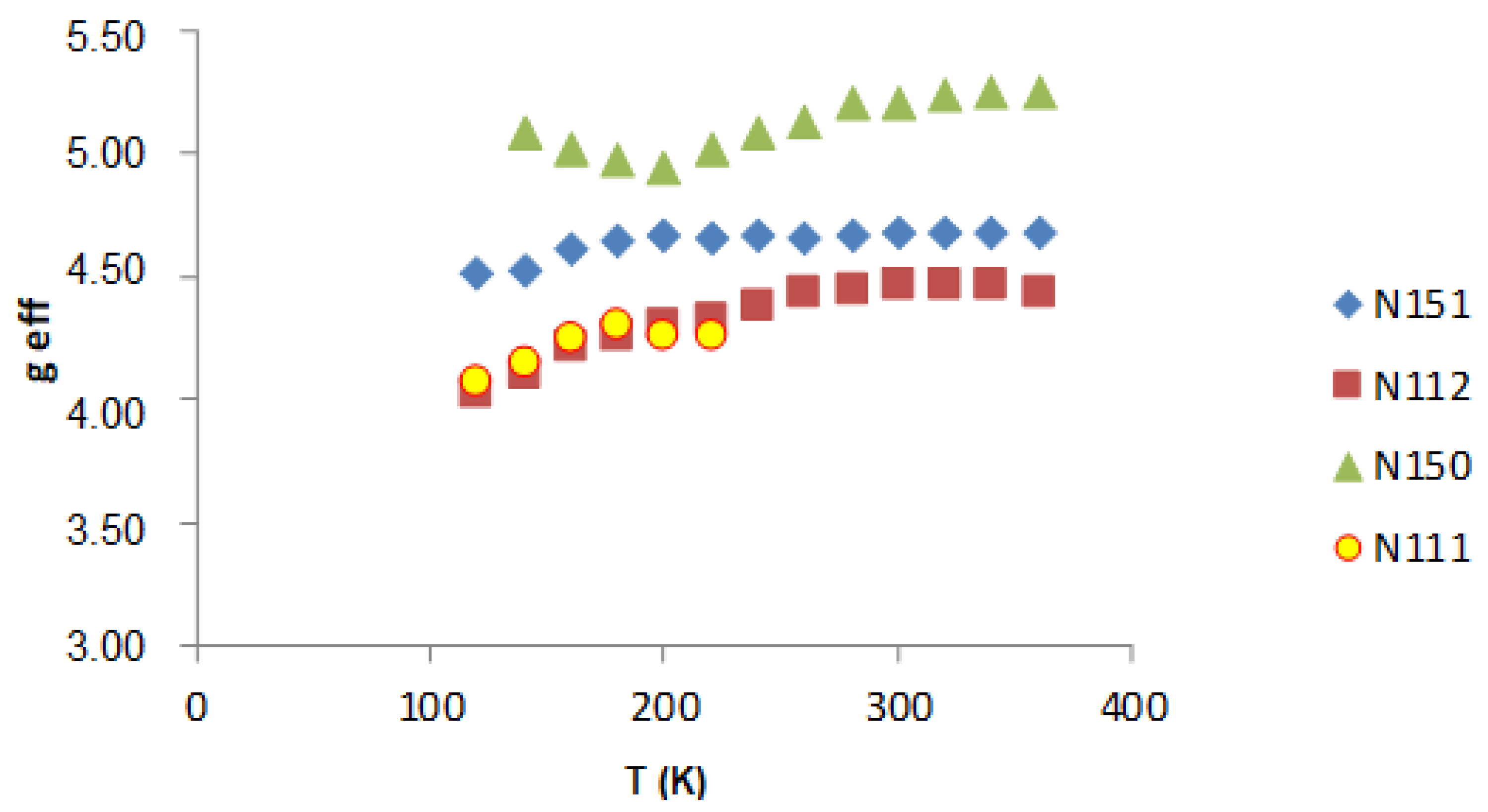
| Magnetic Properties | geff (RT) | ||||
|---|---|---|---|---|---|
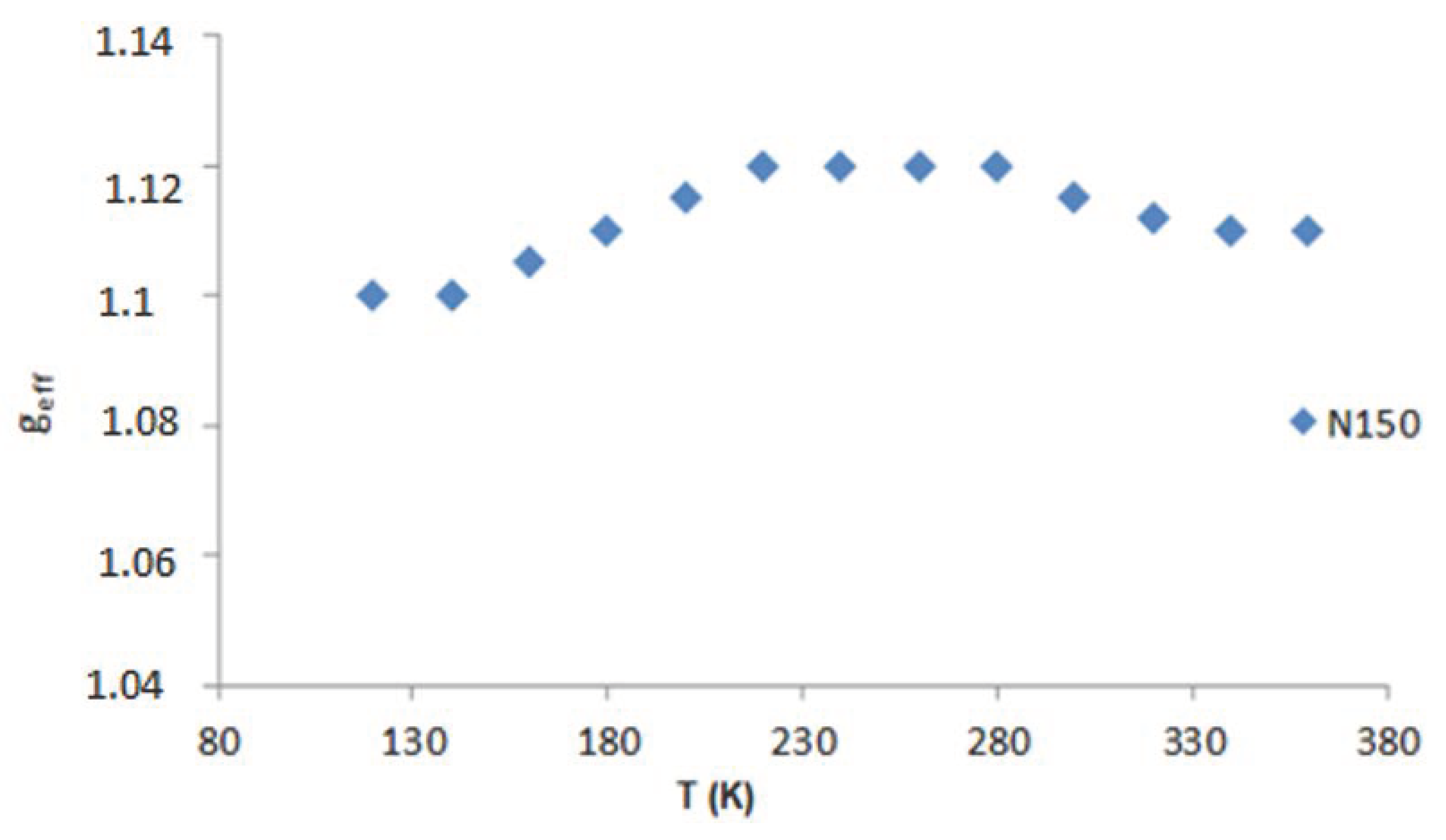
| Sample | Tc(K) | C | “Ferromagnetic” Line (geff ≈ 5) | Pb3+ (geff ≈ 2) | Pb1+ (geff ≈ 1.1) |
| N108 | - | - | 2.14 | ||
| N150 | 75.83 | 3.31 × 10⁷ | 5.20 | 2.07 | 1.115 |
| N151 | 132.99 | 1.94 × 10⁶ | 4.67 | 2.36 | |
| N112 | 5.31 | 1.79 × 10⁸ | 4.46 | 2.39 | |
| N111 | 174.21 | 1.59 × 10¹⁰ | - | 2.11 | |
| N111 | N112 | N150 | N151 | N108 | |
|---|---|---|---|---|---|
| PbTe | PbTe | PbTe | PbTe:In | PbSe | |
| Ts(°C) | 120 | 200 | 300 | 250 | 220 |
| Time (min) | 20 | 25 | 25 | 30 | 25 |
| Numberofpulses | 400 | 500 | 500 | 600 | 500 |
| N110 | N158 | N160 | |
|---|---|---|---|
| PbTe | PbTe:In | PbSe | |
| Ts(°C) | 200 | 200 | 200 |
| Time (min) | 25 | 45 | 45 |
| Numberofpulses | 300 | 550 | 550 |
Publisher’s Note: MDPI stays neutral with regard to jurisdictional claims in published maps and institutional affiliations. |
© 2022 by the authors. Licensee MDPI, Basel, Switzerland. This article is an open access article distributed under the terms and conditions of the Creative Commons Attribution (CC BY) license (https://creativecommons.org/licenses/by/4.0/).
Share and Cite
Wędrychowicz, A.; Cieniek, B.; Stefaniuk, I.; Virt, I.; Śliwa, R. Electron Paramagnetic Resonance Study of PbSe, PbTe, and PbTe:In Semiconductors Obtained by the Pulsed Laser Deposition Method. Molecules 2022, 27, 4381. https://doi.org/10.3390/molecules27144381
Wędrychowicz A, Cieniek B, Stefaniuk I, Virt I, Śliwa R. Electron Paramagnetic Resonance Study of PbSe, PbTe, and PbTe:In Semiconductors Obtained by the Pulsed Laser Deposition Method. Molecules. 2022; 27(14):4381. https://doi.org/10.3390/molecules27144381
Chicago/Turabian StyleWędrychowicz, Aleksandra, Bogumił Cieniek, Ireneusz Stefaniuk, Ihor Virt, and Romana Śliwa. 2022. "Electron Paramagnetic Resonance Study of PbSe, PbTe, and PbTe:In Semiconductors Obtained by the Pulsed Laser Deposition Method" Molecules 27, no. 14: 4381. https://doi.org/10.3390/molecules27144381
APA StyleWędrychowicz, A., Cieniek, B., Stefaniuk, I., Virt, I., & Śliwa, R. (2022). Electron Paramagnetic Resonance Study of PbSe, PbTe, and PbTe:In Semiconductors Obtained by the Pulsed Laser Deposition Method. Molecules, 27(14), 4381. https://doi.org/10.3390/molecules27144381