Article

Tunning of Templated CuWO4 Nanorods Arrays Thickness to Improve Photoanode Water Splitting

1
Group of Applied Nanophysics (Fachgebiet Angewandte Nanophysik), Institute of Physics & IMN MacroNano®, ZIK Technical University of Ilmenau, 98693 Ilmenau, Germany
2
Department of Physics, Faculty of Sciences and Data Analytic, Sepuluh Nopember Technology Institute, Surabaya 60111, Indonesia
3
Department of Physics, Faculty of Sciences, University of Jiangsu, Zhenjiang 212013, China
4
Semiconductor Materials Science Key Laboratory, Semiconductors Institute, Chinese Sciences Academy, Beijing 100083, China
*
Authors to whom correspondence should be addressed.
Molecules 2021, 26(10), 2900; https://doi.org/10.3390/molecules26102900
Submission received: 9 March 2021 / Revised: 9 May 2021 / Accepted: 10 May 2021 / Published: 13 May 2021
(This article belongs to the Special Issue Recent Advances in Water/Solid Interfaces)

Abstract

:
The fabrication of the photoanode of the n-type CuWO4 nanorod arrays was successfully carried out through electrochemical deposition using anodic aluminum oxide (AAO) control templates and for the first time produced distinct gaps between the nanorod arrays. The effectiveness and efficiency of the resulting deposition was shown by the performance of the photoelectrochemical (PEC) procedure with a current density of 1.02 mA cm−2 with irradiation using standard AM 1.5G solar simulator and electron changed radiation of 0.72% with a bias potential of 0.71 V (vs. Ag/AgCl). The gap between each nanorod indicated an optimization of the electrolyte penetration on the interface, which resulted in the expansion of the current density as much as 0.5 × 1024 cm−3 with a flat band potential of 0.14 V vs. Ag/AgCl and also a peak quantum efficiency of wavelength 410 nm. Thus, also indicating the gaps between the nanorod arrays is a promising structure to optimize the performance of the PEC water splitting procedure as a sustainable energy source.

1. Introduction

The world is always in need of energy; however, important nonrenewable energy sources have decreased in recent decades. As a result, researchers have been urged to grow new, sustainable, and environmentally friendly energy sources. In 1972, Fujisima and Honda initiated significant progress on inexpensive and renewable energy technology based on the ecofriendly TiO2 that successfully used solar power [1]. In addition, several exploitations and explorations of many other materials [2], structural repair [3], as well as fabrication techniques have been carried out to increase the performance and quality of a wide range of solar power transformation conversion tools [4,5]. One that is worth examining is the creation of hydrogen fuel using the PEC water splitting procedure that has been proven to be affordable and eco-friendly. Gratzel et al. [6] along with other researchers [7,8] have realized effective materials such as BiFe2O3, CuBiO4, CuWO4, as well as others in the form of multilayer thin films for the application of PEC. However, the numerous layers in these films impede the viability of the application of PEC due to the fact that it must fit the bandgap (in the effective range between 1.6 eV up to 3.2 eV) and also the fabrication and deposition of the materials within a film significantly determines the quality and outcome of mobility, electron majority (type n), hole majority (type p), optical absorption, and adequate resistance.
Tungstate oxide (WO3) is a fascinating substance to investigate since it has high potential in the fields of optical, optoelectronic, diamagnetic, photocatalyst, and sensor [9,10,11]. One particular model for tungstate is copper tungstate oxide (CuWO4). To date, most of the publications on CuWO4 thin film using a bandgap in the ranges of 1.8 eV up to 2.4 eV are feasible to be used as the main material for the application of PEC by using various techniques of deposition, as shown by Martin et al. [12], that reported the deposition of WO4 on Cu. Despite the many publications on CuWO4 thin films, there has been no publication that has reported on obtaining the theoretical CuWO4 efficiency value of 13%.
The creation of electrodes is thicker through the process of sol–gel or electrodeposition and causes a low external quantum efficiency [13]. Moreover, balanced development in CuWO4 nanostructure is assumed to increase the efficiency of light immersion and expand the contact surface zone, thus improving the performance of PEC. Despite the capacity of CuWO4 in efficiently transferring holes on the interface of the electrolyte–material by diffusing in an axial direction, the small electron mobility of CuWO4 impedes the viability of transferring electrons in a radial direction to the current collector [14]. Nanoarrays are an alternative to overcome this problem because the core materials that form these nanoarrays can effectively function as electron separators and transport the current in the axial direction [13]. This novel approach of fabricating CuWO4 in nanostructure form aims to increase the efficiency of visible light absorption (UV–Vis) and the stability of the material. On the other hand, the fabrication of this material has a sequential and complex multistep process and requires a qualitative optimization approach toward the current of the charge carrier in forming the nanostructure [15].
This research has successfully fabricated CuWO4 nanorod arrays through electrodeposition of CuWO4 using nanoimprinted AAO patterns with a constant current of 0.4 mA cm−2. The imprinted AAO template is a simple technology that involves an electrochemical process in the formation process; however, it is relatively cheaper by the anodizing process so that the width and depth of the imprinted template AAO are easy to control, which makes this technology able to produce various nanostructures [16]. By utilizing the control of imprinted AAO templates, distinct gaps between the CuWO4 nanorod arrays are obtained and used as a photoanode for the PEC water splitting procedure. The simulation of electric field distribution on CuWO4 has been carried out in previous research [17]. The resulting CuWO4 nanorod arrays were then tested using a solar simulator (100 mW cm−2) to measure and compare the electrode performance and the theoretical efficiency between CuWO4 nanorod arrays that possess distinct gaps between the arrays and CuWO4 thin films.

2. Materials and Methods

2.1. Materials and Chemicals

Copper(II) nitrate trihydrate (Cu(NO3)2.nH2O) (98%), peroxotungstic acid (H2W2O11) (95%), nickel(II) sulfate (NiSO4) (98%), nickel(II) chloride (NiCl2) (98%), boric acid (H3BO3) (97%), sodium hydroxide (NaOH) (99%), titanium tetrachloride (TiCl4) (99%), phosphoric acid (H3PO4) (70%), sodium sulfate (Na2SO4) (≥99%), copper(II) chloride (CuCl2) (98%), and acetone (C3H6O) (99.8%) were utilized as obtained from Sigma Aldrich. The Loctite 3430 insulating epoxy was used. Thick Al foil (99.99%) and Copper Cu tape (AT528) was acquired from Advance Tapes., while the TEC-15 fluorine-doped tin oxide (FTO) glass (density: 150 nm/1.1 mm; resistivity of sheet: ≤20 Ω/cm2, transmissivity: 88.9% wavelength 400 nm) was bought from NGS Glass.

2.2. Manufacture of Ni Nanopore Arrays

The procedure of creating the pores from the Al nickel (Ni) pore arrays sheet is pressed in order to obtain a round shape with a diameter of 3 cm, then washed cleaned with acetone (99%) in ultrasonic and DI water for 30 min. Furthermore, form Al polishing with the electrochemical method (with applied voltage 30 V) by using a solution of HClO4 and ethanol with a solution ratio of 1:7 accordingly. Then, Once the Ni sheet stem is placed on the Al, which, after polishing using a pressure of 3 kPa for 3 min, will produce a regular pattern on the Al surface. The anodization procedure was carried out at a temperature of 4 °C for 1 h with a voltage of 160 V. This is known as the alumina anodization process of oxide or AAO template forming. Then, to expand the AAO pores following the anodization procedure, the AAO template was submerged in a solution of 5 wt% H3PO4. This submerging process was carried out to control the width of the gap of the AAO template by varying the length of time it was submerged in the solution, which, in turn, produces different width of the gap. The next step was to clean and dry the imprinted AAO template before Au deposition in the range of 20 nm up to 25 nm using an electron beam on the Au at a minimal vacuum condition of 10−3 Torr.

2.3. CuWO4 Synthetics

All reactors were purchased and used without further purification. The materials used were the materials used by Gaillard et al. [18], which consisted of a composition of 25 mM Cu(NO3)2.nH2O and 25 mM H2W2O11. Peroxytungstate solution was obtained by dissolving tungsten metal powder into 10 mL dionixide (DI) water, which consisted of 30% part hydrogen peroxide. Then, as much as 25 mM of these two base solutions were blended in 70:30 DI water: 2-propanol proportion and finished by utilizing 10% nitric acid solution to control the pH of the solution in its final state.

2.4. CuWO4 Nanorod Arrays, and Thin Films Deposition

CuWO4 nanorod arrays was deposited over the AAO template preparation, which were covered by TiO2/Au and CuWO4 thin films on FTO glass by utilizing constant current applied electrodeposition ‒1 mA versus Ag/AgCl for an hour at 30 °C (situ controller) by utilizing Biologic channel. This preparation was then heated at 550 °C for 2 h with an MTI furnace box and was left until arriving at room temperature. The subsequent stage was Ni deposition (0.38 M NiSO4, 0.12 M NiCl2, and 0.3 M H3BO3) by electrodeposition with constant applied potential −10 V for 3 h, accompanied by discarding the posterior layer with CuCl2 solution (26.21 g Cu2SO4, 36 mL HCl, and 700 mL DI water). To exclude the AAO template, 10 wt% H3PO4 was used at 30 °C for 2 h. To secure CuWO4 nanocore arrays, TiO2 was deposited with atomic layer deposition (a Picosun Sunale R150 ALD reactor) on 5 nm density at 200 °C. The titanium dioxide had been deposited by utilizing titanium (IV) chloride (TiCl4) and distilled water (H2O) as Ti and O forerunners, respectively. Then, TiO2 deposition was completed at 200 °C as well as a common cycle comprised TiCl4-N2 purge-H2O-N2 purge (1 cycle). The development pace of TiO2 was around 0.6 nm per cycle.

2.5. CuWO4 Characterizations and PEC Measurement

The energy-dispersive X-ray (EDX) mapping was observed on an S4800 HITACHI (Japan) field emission scanning electron microscope. The morphologies were obtained with a JEM-2100F transmission electron microscope (TEM) operated at an acceleration voltage of 100 kV. High-resolution transmission electron microscopy (HRTEM) images and the corresponding selected area electron diffraction (SAED) analysis were attained at an acceleration voltage of 200 kV. The X-ray diffraction (XRD) patterns were recorded on a Bruker D8 Advance diffractometer equipped with a graphite monochromatized high-intensity Cu Ka radiation (1.54178 Å). The UV–Vis absorption spectra were obtained using a Varian Cary 5000 UV–Vis–NIR spectrophotometer. The EQY was carried out under 150 W from a xenon lamp (controlled by TRACQ BASIC software and connected via Merlin radiometry digital lock-in system) inside a monochromator grating. Current–potential plots and impedance characterization were carried out using the digital BioLogic potentiostat (SP-200) and sodium sulfate with a concentration of 0.1 M as the solution. A Pt counter electrode and an Ag/AgCl reference electrode were used during the measurements.

3. Results and Discussion

To date, the nanoimprinted AAO template method transformed into one of the best advancements that have been demonstrated to significantly contribute to a decent fabrication of nanostructure arrays [19,20] and is also relatively low cost [21] and simple to construct [22]. Figure 1 shows a detailed schematic step-by-step fabrication of the CuWO4 nanorod arrays. The first step of this fabrication is using Ni sheet as the self-support on aluminum. The second step is anodization for as long as 30 min, submerged in an H3PO4 (5 wt%) solution with control pores between 100 nm and 200 nm. Figure 2a–c shows the SEM images of the AAO template and is an overview of the gap between two pores that is dependent on the length of time it was submerged in the H3PO4 (5 wt%) solution. The third step is the deposition of TiO2 and Au. The fourth step is electrodeposition using three electrodes with a potential bias of −0.4 V versus Ag/AgCl and annealing at a temperature of 500 °C for 2 h. The fifth step is nickel plating and the sixth step is the removal of the back side of the AAO template. The last step is the removal of the template by submerging in an H3PO4 (5 wt%) solution for 3 h and at a temperature of 30 °C. A TiO2 5 nm coating layer is added to all the samples using atomic layer deposition (ALD).
The CuWO4 nanorod arrays obtained from AAO are shown in Figure 2d,e. It can be seen that the morphology of the CuWO4 nanorod arrays is well organized due to the high structure control of AAO. The length of the nanorod arrays that are relatively equivalent, in the range between 1 µm and 1.2 µm, and the relatively wide gap between two CuWO4 nanorod arrays will significantly affect the performance of PEC. Electrolyte penetration can easily work on CuWO4 nanorod arrays due to the absence of obstacles, resulting in a high hole and electron mobility. In addition, another advantage of AAO is the low contamination effect even when heated with CuWO4 at temperatures exceeding 550 °C. SEM images shown in Figure 2b,c clearly show no trace of AAO, which is proof that this way is very efficacious for the fabrication of this material and producing gaps between the CuWO4 nanorod arrays of 50 nm, 100 nm, 150 nm, and 200 nm, respectively.
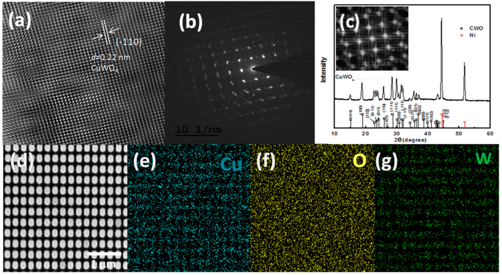
Figure 3a shows us the HRTEM images and SAED patterns of the CuWO4 nanorod arrays with a nanorod array structure diameter of 200 nm, similar to that of previously reported CuWO4 thin films. This is an important basis to propose a concept that irradiation can simply penetrate the surface and the gaps between the CuWO4 nanorod arrays, thus causing a hydrogen evolution reaction in the counter electrode, and at the same time, an oxygen evolution reaction occurs in the CuWO4 nanorod arrays. This is different from CuWO4 thin films in which irradiation only occurs on the surface. To make the results of this research more credible, in Figure 3b, a detailed electron diffraction tomography of the CuWO4 nanorod arrays is shown to obtain a standard structure with a cmcm space group and unit cell parameter of a = 3.72 Å, b = 5.51 Å, and c = 3.98 Å. A high-quality single-crystal appears in this image, as was also visible in the structure of previous research. Furthermore, also shown in Figure 3b, HRTEM using an aberration corrector on the projected crystal quality samples shows that the average gap that is formed between adjacent lattices is 0.22 nm, which in accordance with the area of the material (−110). This also gives information about the high crystallinity consistency, structure, and distribution of Cu and W within the CuWO4 nanorod arrays. Subsequently, complimentary information about the elements from the fast Fourier transform (FFT) simulation is clearly shown in Figure 3c, in which the atom O is randomly distributed in the structure that was formed. The XRD pattern of the electrode is shown in Figure 3c, along with the Miller index of the single-crystal structure. For comparison, measurements were performed to both CuWO4 thin films and CuWO4 nanorod arrays where both samples were heated in air at a temperature of 550 °C for 2 h, and as a result of this fabrication method, XRD patterns are formed on the material [11,19], where the area of the formed CuWO4 nanorod arrays material (001) is at a 24.21° angle and the area of the material (002) reflects an angle of 33.27°. To confirm the chemical composition of the CuWO4 nanorod arrays further, an energy-dispersive X-ray (EDX) mapping is carried out on the constituent particles and is shown in Figure 3e–g, based on the SEM image shown in Figure 3d, and by giving the sequential signal information of Cu, W, and O. The increased crystal quality may be due to the thin coating layer of TiO2 on the imprinted AAO templates that can supply an evenly distributed electric field and activation energy for electrochemical deposition to form the CuWO4 nanorod arrays. Additionally, the thin coating layer of TiO2 can be useful to reduce resistance. The composition from one of the CuWO4 nanorod array samples was identified using X-ray photoelectron spectroscopy (XPS) likewise to that depicted in standard SI W6+ [10]. The Cu (2p) spectrum region is shown by a Cu (2p 3/2) peak and a Cu (2p 1/2) at 933.8 eV and 954.9 eV, respectively, which is also known as the Cu2+ energy peak [12]. Lastly, the O area (1s) that is shown with one peak (1s) is the oxide lattice domain and is generally used to depict the surface of hydroxide on the surface of metal oxide.
The distribution of the gaps between the CuWO4 nanorod arrays for 50 nm, 100 nm, 150 nm, and 200 nm is, respectively, shown in Figure 4a1–a4. It can be seen that for 50 nm the gaps between the CuWO4 nanorod arrays are in the range of 48 nm up to 54 nm (Figure 4a1), for 100 nm, the gaps are in the range of 94 nm up to 102 nm (Figure 4a2), for 150 nm, the gaps are in the range of 148 nm up to 152 nm (Figure 4a3), and for 200 nm, the gaps are in the range of 198 nm up to 202 nm (Figure 4a4). This shows that the nanoimprinted AAO template is an effective technology in controlling CuWO4 to become a nanostructure, which has never been performed previously. The result of the light absorber measurement using UV–Vis spectrophotometry on each distinct gap between the CuWO4 nanorod arrays is shown in Figure 4b. The results present an optimal condition that is obtained by each compartment, thus becoming the basis to claim an increased performance of the PEC water splitting procedure on these CuWO4 nanorod arrays. The light absorber measurement carried out on the distinct gaps between the CuWO4 nanorod arrays, in theory, provides a good chance to optimize the incoming light absorption ability of the photoanode. The absorption spectrum of the samples shown in Figure 4b, shows an increase in incoming light absorption on wavelengths in the range of 300 nm up to 620 nm, which is related to the antireflection characteristic of the CuWO4 nanorod array structure. Furthermore, the absorption spectrum of the CuWO4 nanorod arrays shown in Figure 4b presents absorption in the visible light range. Absorption tends to happen at around 500 nm for gaps between the CuWO4 nanorod arrays of 50 nm and around 620 nm for gaps between the CuWO4 nanorod arrays of 150 nm, which shows that the absorption originates from the CuWO4 material.
To test the maximum carrier generation and the minimum carrier recombination of the CuWO4 nanorod arrays on all the samples with distinct gaps between the CuWO4 nanorod arrays, the PEC measurement was carried out on the photoanode of the CuWO4 nanorod array and is shown in Figure 4c. The working electrode measurement of the CuWO4 nanorod arrays was carried out using three electrodes with an Ag/AgCl electrode reference and a Pt plate as the counter electrode. All the measurements were performed in 0.1 M Na2SO4 (pH 6.8). This procedure was conducted to minimalize the effects of outside bubbles that may occur during the measurement due to irradiation using a solar simulator.
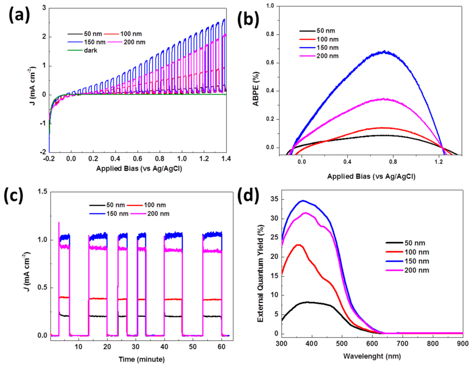
Figure 5a shows the characteristics of current density from irradiation on the photoanode of the CuWO4 nanorod arrays versus the bias potential interval (J-V) that is measured at a potential rate of 20 mV s−1 and a potential range between −0.2 V to 1.4 V vs. Ag/AgCl in dark condition (shown by the green line) and an irradiation of AM 1.5 G, 100 mW cm−2 on the photoanode of the CuWO4 nanorod arrays. All the samples with distinct in-between gaps and diameters (shown in the SEM image in Figure 2) were tested using the previously described measurement. The images clearly show an increase in irradiation current in areas with a positive bias voltage, which shows that CuWO4 nanorod arrays are type-n semiconductors. For comparison, in the images given in Figure S2 of the Supplementary Materials, all the measured samples of the CuWO4 nanorod arrays show the same working area, which is in the positive voltage area. The fundamental difference that can be observed from this measurement is the magnitude of irradiation current density at intervals between 0 V and 0.4 V vs. Ag/AgCl. As described in previous research, there exists a possibility that a transient effect occurs between the standing current and membrane caused by an imperfect bonding between the particles of CuWO4 that causes a decrease in the current density of the irradiation. Therefore, adding a very thin layer of TiO2, approximately around ±5 nm (Egap TiO2 3.2 eV) using ALD on the surface of the CuWO4 nanorod arrays, may increase the capacity of the light absorption spectrum of the CuWO4 nanorod arrays. This is despite previous research findings, in which the photoanode of CuWO4 obtained a maximum value of 3% to change the incoming light irradiation to hydrogen due to the large energy gap between the valence band and the conduction band. Nevertheless, the presence of the Au particles from the beginning of the fabrication process of the imprinted AAO template can also cause a surface plasmon resonance (SPR) effect. Hales et al. stated that the magnitude of the SPR effect depends on the size, morphology, and density of the Au particles [23]. The Au particles that are scattered on the surface of the photoanode are also used as a conductor for the deposition of the CuWO4 nanorod arrays in the early phase, as mentioned in the steps in Figure 1. For comparison, Figure S2 of the Supplementary Materials shows the photogenerated measurement on CuWO4 thin films. CuWO4 thin films were deposited on FTO glass with the same mechanism as the fabrication method of the CuWO4 nanorod arrays. Likewise, the photogenerated measurement on CuWO4 thin films used the same electrolyte and bias voltage limit range. It is clearly shown in Figure S2 of the Supplementary Materials that the maximum irradiation current density of the applied bias potential thermodynamics is around 0.74 mA cm−2, which is lower than the same measurement performed on the compartments of the CuWO4 nanorod arrays. The logical reasoning behind this is that hole injection on CuWO4 thin films to slow electrolytes and the weak current carrier enables the CuWO4 thin films to have a lower performance toward its PEC water splitting measurement.
Figure 4 nanorod arrays using the equation, which is η = J(1.23 − Vapp)/Plight, where Vapp applies a bias potential vs. Ag/AgCl, J is the external current density, and Plight is the irradiation power. The results of the measurement are presented in Figure 5b, showing a measurement of 0.06% (at 0.681 V vs. Ag/AgCl), 0.12% (at 0.683 V vs. Ag/AgCl), 0.72% (at 0.712 V vs. Ag/AgCl), and 0.38% (at 0.711 V vs. Ag/AgCl) for gaps between the CuWO4 nanorod arrays of 50 nm, 100 nm, 150 nm, and 200 nm, respectively. From the measurements presented in Figure 5b, it can be seen that the optimal electrode gap between the CuWO4 nanorod arrays is 150 nm. As a result, the composition of the CuWO4 nanorod arrays has a wider layer and is in direct contact with the electrolyte and, in turn, serves as an effective conductor of electrons from the interface of the working electrode to the counter electrode and vice versa, causing a quick charge transfer. Nevertheless, a gap too close or too far between two diamagnetic CuWO4 nanorod arrays can significantly affect the created electric field [24]. As a result, an optimal gap can have a significant effect on this diamagnetic material. Qualitatively, it can be interpreted that polarization of the induction current and the noncarrier of the magnetic field orbit can efficiently influence the irradiation conversion. As shown in Figure 5c, the characteristics of AM 1.5G irradiation on the CuWO4 nanorod arrays seem relatively stable within 60 min and in a dark–light condition. When the current resulted from irradiation reaches a value of 1.02 mA cm−2 with 0.7 V vs. Ag/AgCl, this result is a significant improvement, compared to previous research. For comparison, we show the measurement of current irradiation of CuWO4 thin films in Figure S3 of the Supplementary Materials. This verifies our hypothesis that the photoanode of the CuWO4 nanorod arrays significantly influences photogeneration, which is shown by CuWO4 nanorod arrays exhibiting an absorption and photon collection through the bandgap transition between electrodes. The highest value comes from the electrode with an in-between gap of 150 nm, corresponding to the highest absorption curve shown in Figure 4b.
As for the EQY (%) measurement on the photoanode of the CuWO4 nanorod arrays for every sample, the measurement is carried out without the use of bias voltage, as shown in Figure 5d. The EQY peak occurs at wavelengths around 410 nm. For additional information, this photon-to-current peak efficiency occurs for all the samples with distinct gaps between the CuWO4 nanorod arrays. As stated before, the effect of the gap between the CuWO4 nanorod arrays is very transparent. A close gap between the CuWO4 nanorod arrays significantly influences a decrease in the efficiency value of the measurement. As a result, photon absorption of electrodes is effective within the relatively wide wavelength interval of visible light, which is in the range of 300 nm up to 620 nm. This is proof that nanostructures can significantly influence an increased response toward incoming light at wavelengths between 300 nm and 620 nm. The effect of the gap between the CuWO4 nanorod arrays significantly impacts the performance of this photoelectrode.
Next, a measurement to describe the electronic structure of the CuWO4 nanorod arrays composite is needed. For this, a relevant Mott–Schottky (M–S) plot is used and also by observing the electrochemical impedance, which, in this research, starts from a frequency of 1 Hz up to 1 MHz with a bias potential interval of −0.4 V up to +0.7 V vs. Ag/AgCl. The capacitance value of the measurement is presented in Figure 6a at a frequency of 1 kHz. From this, it is shown that the M–S plot from each electrode with a distinct gap between the CuWO4 nanorod arrays in the PEC water splitting procedure has a linear profile and a positive slope that demonstrates features of a type-n semiconductor. These data are then used for the M–S relation, in which the typical potential of the flat band VFB is in the range of 0.2 V vs. Ag/AgCl up to 0.19 V vs. Ag/AgCl, which is in reference to previous research [24,25]. From the results, we obtained a plot and is linearly projected on each distinct flat bond potential of −0.16 V (vs. Ag/AgCl), −0.14 V (vs. Ag/AgCl), −0.104 V (vs. Ag/AgCl), and 0.46 V (vs. Ag/AgCl) in the open-circuit voltage under 100 mW cm−2 irradiation for each electrode with distinct gaps between the CuWO4 nanorod arrays of 50 nm, 100 nm, 150, and 200 nm, respectively. Then, the density of the majority charge carrier is calculated from the gradient of the M–S plot by using the equation d(Csc−2)/dE = 2/oεND, where the dielectric constant is 83 for the CuWO4 nanorod arrays and the effective electron mass is 70 [24,26]. From the calculation, the density of the majority charge carrier of 0.84 × 1020 cm−3, 0.97 × 1020 cm−3, 2.86 × 1020 cm−3, and 1.35 × 1020 cm−3 are obtained for distinct gaps between the CuWO4 nanorod arrays of 50 nm, 100 nm, 150, and 200 nm, respectively. The results show a higher majority charge carrier than that reported in previous research [24,26]. Figure 6a also clearly demonstrates that the CuWO4 nanorod arrays have the behavior and conductivity of a type-n semiconductor, and the highest value of the majority charge carrier belongs to the CuWO4 nanorod array with an in-between gap of 150 nm. As shown in the inset of Figure 6a, the Nyquist plot is measured in the frequency range of 106 Hz up to 1 MHz with a bias of 0 V vs. Ag/AgCl for two sets of electrodes in PEC. In addition, this is to show that a Nyquist plot resulting in a half circle at the highest frequency is the fundamental characteristic of the process of charge transfer throughout the process of measurement. Furthermore, the diameter of the half circle formed by the Nyquist plot is relatively equal to the charge transfer resistance [27]. The overall electrochemical measurements show that the modification of the CuWO4 nanorod arrays has a positive impact on the electronic nature of the CuWO4, which is indicated by the increase in doping density and area of band banding on the interface of the photoanode and electrolyte. Additionally, an observation on charge transfer resistance can be made on the overall electrochemical measurements, that is, the smaller the resistance, the more useful it is to promote charge separation in water molecules and charge carrier transfer as a result of irradiation. This provides a higher efficiency signal for utilizing charge generated from photogeneration of the CuWO4 nanorod arrays, compared to that of CuWO4 thin films.
On the other hand, determining the proper bandgap of the CuWO4 nanorod arrays based on bandgap values obtained using the Tauc plot method is shown in Figure 6b. It is known that a water splitting reaction must be at the right range of standard reduction and oxidation potential because CuWO4 nanorod arrays have valence bands and conduction bands within that range, thus making CuWO4 nanorod arrays a very good material for the PEC water splitting procedure. To summarize, the small distance between the Fermi level and the valence band indicates that CuWO4 nanorod arrays are the desired type-n semiconductor. The estimated bandgap has a slightly lower value than that of previous research that is closely related to material defect [13], in which the energy was obtained in vacuum conditions, and surface defect was disregarded through an ion milling procedure. This procedure causes a significant difference in bandgap that is measured with the electrochemical technique, compared to the procedure that we carried out.
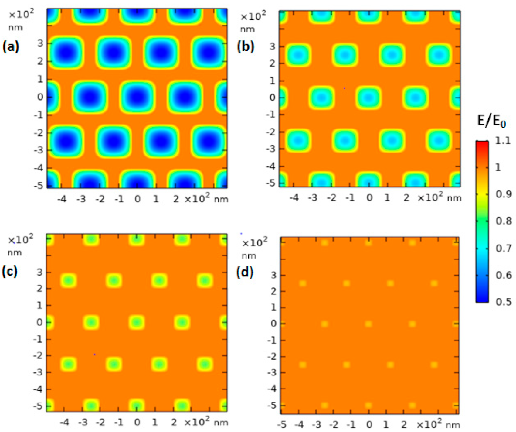
We carried out a simulation of the selected material to further understand the interaction between the photon and the CuWO4 nanorod arrays using the FDTD method and is shown in Figure 7 for each distinct gap between the CuWO4 nanorod arrays. From the outcome of this simulation, information on the electric field distribution of photon irradiation with a specific wavelength of 410 nm on areas of the CuWO4 nanorod arrays is obtained and captured from the top layer. The distinct gaps between the CuWO4 nanorod arrays observed ranged from small to large gaps. The density of electric field coupling on all types of material can produce a strong energy contour, thus having a big influence on the efficiency signal of spectroscopy. As a result, the distribution of the CuWO4 nanorod arrays produced by the scattering of the nanorod arrays is in line with nano metal particle arrays. Jain et al. [28] explained that bipolar coupling caused by the in-between gaps will result in a decay of the plasmon coupling, and this will become irrelevant on metal, material form, and the dielectric constant of all types of material. Moreover, the increase of intensity in the near field indicates a faster decay as the gap of the CuWO4 nanorod arrays becomes bigger. In other words, if the gaps between the CuWO4 nanorod arrays are made to be bigger, then the electric field coupling becomes weaker. This weakening of the coupling may be one of the reasons a bandgap shift occurs in the CuWO4 nanorod arrays. However, the bandgap shift that occurs in the CuWO4 nanorod arrays can be controlled by setting the gaps between the CuWO4 nanorod arrays of the samples to 150 nm and 200 nm based on the conventional quantum confinement effect. In other words, the results give information that a bandgap shift can be achieved by controlling the diameter and the in-between gaps on the conventional quantum confinement effect even though the obtained parameters are relatively bigger than that of the Bohr radius. Due to the reasons above, along with the relative energy density of the CuWO4 nanorod arrays, which is not significantly different, the quantum effect shows that a cumulative change in thickness of the CuWO4 nanorod arrays is not accounted for. However, the bandgap shift is specifically tied to the interaction between the CuWO4 nanorod arrays after irradiation and the uniformity of the structure of the material. The stability of the bandgap is in relevance to the power of the near-field light, where this is used to increase the advantages of the optical properties of the CuWO4 nanorod arrays to be used as material for the application of photoelectric.
The FDTD simulation on the CuWO4 nanorod arrays gives information on the interaction connection between the photon and the geometric parameter of the CuWO4 nanorod arrays that possess distinct gaps between the arrays, thus resulting in optimal electric field intensity. The simulation that was taken from irradiation on the top layer of the CuWO4 nanorod arrays shows the abundant distribution of counter anode along the layer that differentiates CuWO4 nanorod arrays with the medium. It can be seen in Figure 7 (also see Figure S3 of the Supplementary Materials) that as the gaps between the CuWO4 nanorod arrays become bigger, the electric field becomes weaker; both of them were carried out at close to 700 nm. Likewise, as the gaps between the CuWO4 nanorod arrays become smaller, the electric field becomes stronger. Nevertheless, the electric field that occurs on the CuWO4 nanorod arrays also affects the magnetic field; thus, it has relevance toward the penetration of the electron charge of electrolytes on the CuWO4 nanorod arrays. As a result, a suitable gap between the CuWO4 nanorod arrays is needed to obtain a magnetic field and an electric field that significantly contributes toward the performance of the PEC water splitting procedure. The results of this experiment and simulation clearly show that CuWO4 nanorod arrays greatly contribute toward the efficiency of CuWO4 thin films.

4. Conclusions

In conclusion, to the best of our knowledge, this is the first time that the fabrication of CuWO4 nanorod arrays using imprinted AAO templates by electrodeposition was carried out. The photoanode of the CuWO4 nanorod arrays was fabricated with four distinct gap variations and is what makes it superior to other compartments such as CuWO4 thin films. It is proven that with this method, the fabricated CuWO4 nanorod arrays show a high degree of material purity when tested using XRD and XPS. Additionally, when observed with SEM and EDX, it is proven that the CuWO4 nanorod arrays material structure can be controlled and also produce a chemical structure from its three-molecule compound composition. A realization of CuWO4 nanorod arrays that have a homogenous structure and have suitable gaps between the CuWO4 nanorod arrays is key to optimizing the penetration of charge between electrolyte and photoanode to absorb incoming photons from irradiation of 100 mW cm−2. The maximum photogeneration of the CuWO4 nanorod arrays was obtained at a gap between the CuWO4 nanorod arrays of 150 nm and a current density of 1.01 mA cm−2, which resulted in an APBE peak at a bias voltage of 0.7 V vs. Ag/AgCl. The results of this research are further strengthened by an FDTD simulation that generated magnetic field energy and electric field energy that match the experiment that was carried out, in which the peak energy was contrary to its absorbance at a wavelength of around 700 nm.

Supplementary Materials

The following are available online, Figure S1: XPS survey of CuWO4, core-level XPS of Cu2p, core-level XPS of W 5d, and core-level XPS of O1s, respectively, Figure S2: (a) LSV of a CuWO4 thin film photoanode in a three-electrode configuration described in the text and under AM 1.5 G sunlight. The scans are collected from −0.2 to 1.4 V versus Ag/AgCl. (b) ABPEs of the relevant electrodes from (a), Figure S3: Electric energy and magnetic energy from FDTD simulation by CuWO4 nanorod arrays in the in-between gap, Table S1: Previous report for photoelectrochemical measurements of the kinds CuWO4 photoanode for oxygen evolution reaction.

Author Contributions

Conceptualization, N.N. and Y.L.; methodology, N.N. and D.C.; software, N.N. and U.F.; validation, N.N., Y.L. and Z.W.; formal analysis, N.N. and D.C.; investigation, N.N. and Z.W.; resources, Y.L.; data curation, N.N.; writing—original draft preparation, N.N.; writing—review and editing, Y.L.; visualization, U.F.; supervision, Y.L. and A.R.; project administration, A.R.; funding acquisition, N.N. and A.R. All authors have read and agreed to the published version of the manuscript.

Funding

This research was funded by Ministry of Research and Technology, The Republic of Indonesia (BRIN-RISTEK) DIKTI No.3/AMD/E1/KP.PTNBH/2020.

Institutional Review Board Statement

Not applicable.

Informed Consent Statement

Not applicable.

Data Availability Statement

Not applicable.

Acknowledgments

The authors gratefully acknowledge financial support from the Institut Teknologi Sepuluh Nopember and BRIN-RISTEK DIKTI for this work, under the project scheme of the Publication Writing and IPR Incentive Program (PPHKI). The researcher would also like to express gratitude to Jens Schawohl in ZMN TU Ilmenau for XRD measurements, and Yueliang Li in Ulm University for TEM measurement.

Conflicts of Interest

The authors declare no conflict of interest.

References

  1. Kato, Y.; Koyama, M.; Fukushima, Y.; Nakagaki, T. Energy Technology Roadmaps of Japan: Future Energy Systems Based on Feasible Technologies Beyond 2030; Springer: Tokyo, Japan, 2016; ISBN 978-4-431-55951-1. [Google Scholar]
  2. Kolwas, K.; Derkachova, A. Modification of Solar Energy Harvesting in Photovoltaic Materials by Plasmonic Nanospheres: New Absorption Bands in Perovskite Composite Film. J. Phys. Chem. C 2017, 121, 4524–4539. [Google Scholar] [CrossRef]
  3. Meng, L.; Li, C.; Dos Santos, M. Structural Modification of TiO2 Nanorod Films with an Influence on the Photovoltaic Efficiency of a Dye-Sensitized Solar Cell (DSSC). J. Inorg. Organomet. Polym. Mater. 2013, 23, 787–792. [Google Scholar] [CrossRef] [Green Version]
  4. Miyata, T.; Watanabe, K.; Tokunaga, H.; Minami, T. Photovoltaic Properties of Cu2O-Based Heterojunction Solar Cells Using n-Type Oxide Semiconductor Nano Thin Films Prepared by Low Damage Magnetron Sputtering Method. J. Semicond. 2019, 40, 032701. [Google Scholar] [CrossRef]
  5. Peng, Y.; Gong, S.; Liu, K.; Yao, M. Nano-Sphere Surface Arrays Based on GaAs Solar Cells. J. Semicond. 2020, 41, 012701. [Google Scholar] [CrossRef]
  6. Paracchino, A.; Laporte, V.; Sivula, K.; Grätzel, M.; Thimsen, E. Highly Active Oxide Photocathode for Photoelectrochemical Water Reduction. Nat. Mater. 2011, 10, 456–461. [Google Scholar] [CrossRef]
  7. Thimsen, E.; Le Formal, F.; Grätzel, M.; Warren, S.C. Influence of Plasmonic Au Nanoparticles on the Photoactivity of Fe2O3 Electrodes for Water Splitting. Nano Lett. 2011, 11, 35–43. [Google Scholar] [CrossRef]
  8. Chen, H.; Leng, W.; Xu, Y. Enhanced Visible-Light Photoactivity of CuWO4 through a Surface-Deposited CuO. J. Phys. Chem. C 2014, 118, 9982–9989. [Google Scholar] [CrossRef]
  9. Amano, F.; Li, D.; Ohtani, B. Photoelectrochemical Property of Tungsten Oxide Films of Vertically Aligned Flakes for Visible-Light-Induced Water Oxidation. J. Electrochem. Soc. 2011, 158, K42–K46. [Google Scholar] [CrossRef]
  10. Zhan, F.; Li, J.; Li, W.; Liu, Y.; Xie, R.; Yang, Y.; Li, Y.; Chen, Q. In Situ Formation of CuWO4/WO3 Heterojunction Plates Array Films with Enhanced Photoelectrochemical Properties. Int. J. Hydrog. Energy 2015, 40, 6512–6520. [Google Scholar] [CrossRef]
  11. Bao, M.; Chen, Y.; Li, F.; Ma, J.; Lv, T.; Tang, Y.; Chen, L.; Xu, Z.; Wang, T. Plate-like p–n Heterogeneous NiO/WO3 Nanocomposites for High Performance Room Temperature NO2 Sensors. Nanoscale 2014, 6, 4063–4066. [Google Scholar] [CrossRef]
  12. Denk, M.; Kuhness, D.; Wagner, M.; Surnev, S.; Negreiros, F.R.; Sementa, L.; Barcaro, G.; Vobornik, I.; Fortunelli, A.; Netzer, F.P. Metal Tungstates at the Ultimate Two-Dimensional Limit: Fabrication of a CuWO4 Nanophase. Acs Nano 2014, 8, 3947–3954. [Google Scholar] [CrossRef]
  13. Yourey, J.E.; Pyper, K.J.; Kurtz, J.B.; Bartlett, B.M. Chemical Stability of CuWO4 for Photoelectrochemical Water Oxidation. J. Phys. Chem. C 2013, 117, 8708–8718. [Google Scholar] [CrossRef]
  14. Yourey, J.E.; Bartlett, B.M. Electrochemical Deposition and Photoelectrochemistry of CuWO4, a Promising Photoanode for Water Oxidation. J. Mater. Chem. 2011, 21, 7651–7660. [Google Scholar] [CrossRef]
  15. Wen, L.; Wang, Z.; Mi, Y.; Xu, R.; Yu, S.-H.; Lei, Y. Designing Heterogeneous 1D Nanostructure Arrays Based on AAO Templates for Energy Applications. Small 2015, 11, 3408–3428. [Google Scholar] [CrossRef]
  16. Nasori, N.; Dai, T.; Jia, X.; Rubiyanto, A.; Cao, D.; Qu, S.; Wang, Z.; Wang, Z.; Lei, Y. Realizing Super-Long Cu2O Nanowires Arrays for High-Efficient Water Splitting Applications with a Convenient Approach. J. Semicond. 2019, 40, 052701. [Google Scholar] [CrossRef]
  17. Nasori, N.; Hafida, N.H.; Tahier, A.R.H.; Rubiyanto, A. Effect of Phosphate Buffer Saline Solution on the Performance of Zinc Oxide Thin Film Surface Electrodes Using Electrochemical Detection for Glucose Biosensor. AIP Conf. Proc. 2020, 2296, 020125. [Google Scholar]
  18. Gaillard, N.; Chang, Y.; DeAngelis, A.; Higgins, S.; Braun, A. A Nanocomposite Photoelectrode Made of 2.2 EV Band Gap Copper Tungstate (CuWO4) and Multi-Wall Carbon Nanotubes for Solar-Assisted Water Splitting. Int. J. Hydrogen Energy 2013, 38, 3166–3176. [Google Scholar] [CrossRef]
  19. Zhao, H.; Wang, C.; Vellacheri, R.; Zhou, M.; Xu, Y.; Fu, Q.; Wu, M.; Grote, F.; Lei, Y. Self-Supported Metallic Nanopore Arrays with Highly Oriented Nanoporous Structures as Ideally Nanostructured Electrodes for Supercapacitor Applications. Adv. Mater. 2014, 26, 7654–7659. [Google Scholar] [CrossRef]
  20. Liang, L.; Xu, Y.; Wang, C.; Wen, L.; Fang, Y.; Mi, Y.; Zhou, M.; Zhao, H.; Lei, Y. Large-Scale Highly Ordered Sb Nanorod Array Anodes with High Capacity and Rate Capability for Sodium-Ion Batteries. Energy Environ. Sci. 2015, 8, 2954–2962. [Google Scholar] [CrossRef]
  21. Wen, L.; Mi, Y.; Wang, C.; Fang, Y.; Grote, F.; Zhao, H.; Zhou, M.; Lei, Y. Cost-Effective Atomic Layer Deposition Synthesis of Pt Nanotube Arrays: Application for High Performance Supercapacitor. Small 2014, 10, 3162–3168. [Google Scholar] [CrossRef]
  22. Zhan, Z.; Lei, Y. Sub-100-Nm Nanoparticle Arrays with Perfect Ordering and Tunable and Uniform Dimensions Fabricated by Combining Nanoimprinting with Ultrathin Alumina Membrane Technique. ACS Nano 2014, 8, 3862–3868. [Google Scholar] [CrossRef] [PubMed]
  23. Hsu, J.; Fuentes-Hernandez, C.; Ernst, A.R.; Hales, J.M.; Perry, J.W.; Kippelen, B. Linear and Nonlinear Optical Properties of Ag/Au Bilayer Thin Films. Opt. Expressoe 2012, 20, 8629–8640. [Google Scholar] [CrossRef] [PubMed]
  24. Hu, D.; Diao, P.; Xu, D.; Xia, M.; Gu, Y.; Wu, Q.; Li, C.; Yang, S. Copper(II) Tungstate Nanoflake Array Films: Sacrificial Template Synthesis, Hydrogen Treatment, and Their Application as Photoanodes in Solar Water Splitting. Nanoscale 2016, 8, 5892–5901. [Google Scholar] [CrossRef] [PubMed]
  25. Mi, Y.; Wen, L.; Xu, R.; Wang, Z.; Cao, D.; Fang, Y.; Lei, Y. Constructing a AZO/TiO2 Core/Shell Nanocone Array with Uniformly Dispersed Au NPs for Enhancing Photoelectrochemical Water Splitting. Adv. Energy Mater. 2016, 6, 1501496. [Google Scholar] [CrossRef]
  26. Xu, Y.; Zhou, M.; Wen, L.; Wang, C.; Zhao, H.; Mi, Y.; Liang, L.; Fu, Q.; Wu, M.; Lei, Y. Highly Ordered Three-Dimensional Ni-TiO2 Nanoarrays as Sodium Ion Battery Anodes. Chem. Mater. 2015, 27, 4274–4280. [Google Scholar] [CrossRef]
  27. Lima, A.E.B.; Costa, M.J.S.; Santos, R.S.; Batista, N.C.; Cavalcante, L.S.; Longo, E.; Lu, G.E., Jr. Facile Preparation of CuWO4 Porous Films and Their Photoelectrochemical Properties. Electrochim. Acta 2017, 256. [Google Scholar] [CrossRef] [Green Version]
  28. Pilli, S.K.; Deutsch, T.G.; Furtak, T.E.; Brown, L.D.; Turner, J.A.; Herring, A.M. BiVO4/CuWO4 Heterojunction Photoanodes for Efficient Solar Driven Water Oxidation. Phys. Chem. Chem. Phys. 2013, 15, 3273–3278. [Google Scholar] [CrossRef]
Figure 1. The sequential phases of the fabrication of the CuWO4 nanocore arrays using an imprinted AAO template with Ni sheet as a substrate to support the photoanode.
Molecules 26 02900 g001
Figure 2. (a) SEM images of the top view of the imprinted AAO template with a highly uniform order; (a1) SEM images of the top view of the imprinted AAO template with a scale of 100 nm; (a2) a side view of the imprinted AAO template; and (be) SEM images of the photoanode of the CuWO4 nanorod arrays with an estimated gap between the CuWO4 nanorod arrays of 50 nm, 100 nm, 150 nm, and 200 nm, respectively.
Molecules 26 02900 g002
Figure 3. (a) High-resolution transmission electron microscopy (HRTEM) image of a sample of the photoanode of the CuWO4 nanorod arrays after deposition; (b) a selected area from the electron diffraction pattern of a sample of the photoanode of the CuWO4 nanorod arrays; (c) XRD pattern of a sample of the photoanode of the CuWO4 nanorod arrays (insert: SAED pattern of a sample of the photoanode of the CuWO4 nanorod arrays, the smaller image shows the inverse FFT cell); and (d) SEM images of the EDX mapping that represent (e) the Cu element, (f) the O element, and (g) the W element, respectively.
Molecules 26 02900 g003
Figure 4. The average measurement of the samples of the photoanode of the CuWO4 nanorod arrays with distinct gaps between the nanorod arrays of (a1) 50 nm, (a2) 100 nm, (a3) 150 nm, and (a4) 200 nm; (b) the absorption measurement within the UV–Vis light range of each photoanode samples; and (c) image of the photoanode of the CuWO4 nanorod arrays covered with epoxy used for the electrical properties testing.
Molecules 26 02900 g004
Figure 5. (a) Illumination of on–off rays with a solar simulator and irradiation of 100 mW cm−2 with a typical LSV (J-V) on the photoanode of the CuWO4 nanorod arrays using three electrodes. The scanning was set with a bias potential in the range of −0.2 up to 1.4 V vs. Ag/AgCl; (b) APBE calculations of each of the samples of the photoanode based on the data shown in (a). (c) the stability measurement of the photoanode of the CuWO4 nanorod arrays (J-t) that was set with a constant potential of 0.7 V vs. Ag/AgCl using a solar simulator and irradiation of 100 mW cm−2 for as long as 1 h; and (d) the EQY measurements for each of the photoanode of the CuWO4 nanorod arrays. All the measurements in Figure 5 were carried out by using an electrolyte of 0.1 M sodium sulfate.
Molecules 26 02900 g005
Figure 6. (a) The Mott‒Schottky plot used to determine the direct voltage of the flat band for each of the photoanode of the CuWO4 nanorod arrays (the smaller image shows the SPEIS measurement for the Nyquist plot) and (b) the energy level scheme of the photoanode of the CuWO4 nanorod arrays.
Molecules 26 02900 g006
Figure 7. A top view of the FDTD simulation of the photoanode of the CuWO4 nanorod arrays toward EM waves with a wavelength of 420 nm for each of the samples of the photoanode of the CuWO4 nanorod arrays with distinct gaps between the CuWO4 nanorod arrays of (a) 50 nm, (b) 100 nm, (c) 150 nm, and (d) 200 nm.
Molecules 26 02900 g007
Publisher’s Note: MDPI stays neutral with regard to jurisdictional claims in published maps and institutional affiliations.

