1. Introduction
A large number of applications involve Fast Fourier Transform (FFT) computations, especially the processes in the areas of telecommunications, vision and signal processing. The FFT tasks on edge and satellite devices receive input data from sensors and they often need real-time performance. In the edge cases, data transfer to the cloud for processing may delay the results and decision production [
1]. In satellites, the designer either has to forward the data to Earth or increase the cost of the satellite by adding computing resources, e.g., accelerators and memory, which increase the satellite’s volume, cost and power consumption [
2]. An attractive and feasible solution to these two cases is to improve the edge and satellite resource utilization, which in addition may reduce power consumption. We note that most satellites are equipped with processors marked as “space-proven” a term characterizing devices that have a demonstrated history of successful operation in space [
3]. Researchers and engineers proposed in-place FFT techniques for improving resource utilization [
4]. These techniques employ a memory of size equal to the input, which stores initially the input data, then all the intermediate results produced during the FFT stages and finally the output data. The gains are in the memory cost, power consumption, execution time and real-time performance. Moreover, a significant number of these studies propose addressing schemes able to load and store in parallel the butterfly
r-tuple data to/from the processor that implements the radix-
r butterflies [
5,
6]. The latter schemes complete the butterfly computations, and then they shuffle the data among the tuples at each FFT stage by using a variety of permutations [
5,
6,
7]. A plethora of reports for FFT in-place algorithm-specific architectures, such as those in [
5,
6,
7,
8,
9,
10], focus on improving the circuit complexity and gate count for a variety of radixes. The majority of these reports consider the algorithm-specific architectures as accelerators [
5,
7,
9,
10]. However, such accelerators increase the cost and the requirements for volume of a CubeSat or a NanoSat. Compared to a respectable number of papers for algorithm-specific in-place FFT architectures, there is a small number of in-place FFT techniques reported for the Central Processing Units (CPUs) and Digital Signal Processors (DSPs). Most of these propose the use of registers within the processor, which provide the required space for implementing the permutations.
Aiming at improving the FFT execution on edge and space-proven processors with respect to resource utilization, speed and power consumption, the current paper enhances the performance of the radix-2 FFT in-place techniques. The proposed technique benefits from a scheme that stores the two points of each FTT butterfly couple in a single memory address. At each stage, this scheme loads two FFT pairs, one pair per cycle. Upon completion of the two butterfly computations, it permutes the results and stores one pair per cycle, so that in the next stage it will load each pair in a single clock cycle. This data exchange between the two FFT pairs complies with a known straightforward permutation similar to other reports such as that in [
7]. The processors in this work have 32-bit and 64-bit word length. For the FFT computations in processors of 32-bit word length, the proposed method represents the numbers’ real and imaginary parts with 8-bit floating point (FP8) [
11,
12] or 8-bit block floating point (BFP8). For processors of 64-bit word length, it uses FP16 or 16-bit block floating point (BFP16). The contributions of this work are as follows: (a) the design of the code for the in-place FFT that utilizes efficiently the addressing and load/store processors’ resources; (b) improved memory utilization and performance of the radix-2 FFT on space-proven and edge computing devices; and (c) the evaluation of the Signal-to-Noise Ratio (SNR) performance of the FFT using FP8 BFP8, FP16 and BFP16 and the comparison of using these representations for FFT sizes in the range of 1K up to 16K input points. A notable result of this work is the efficient block floating point (BFP) configuration producing improved SNR results in all cases. Organizing a combination of this BFP and the in-place technique significantly improves the following: (a) resource utilization, (b) the execution time for all the FFT executions with BFP number representation, and (c) consequently, the power consumption. This improvement becomes a key advantage of the technique, especially for space-proven and edge devices with limited computational power and memory size. An example is the space-proven AVR32 (AT32UC3C0512C) [
13] which executes an FFT of 16K input points on the processor’s 64 KB memory.
The motivation for this method came from the design and development of the ERMIS 3 CubeSat (8U satellite) project [
14,
15]. CubeSats have limited space, devices of lesser computational power and relatively small memory size. Consequently, the efficiency of fundamental computations, such as the FFT, contributes significantly to Earth Observation (EO) and signal processing tasks. For this purpose, the research team focused on the design of the proposed method for improving the FFT on the AVR32 (the ERMIS 3 On-Board Computer, OBC), also on the space-proven Intel Movidius Myriad 2 (MA2450) [
16] used as a signal-processing accelerator in the European Space Agency’s (ESA) High-Performance Compute Board (HPCB) project [
17] and the Raspberry Pi Zero 2W edge device [
18]. Moreover, this work developed a hardware accelerator designed in Very-High-Speed Integrated Circuit Program Hardware Description Language (VHDL) [
19] on the low-cost edge Field Programmable Gate Array (FPGA) device XC7Z007S [
20] and it compares the accelerator’s performance to that of the aforementioned processing units.
The paper is organized with the following section reporting related results in the literature.
Section 3 describes the methods, the code and the processing devices and platforms.
Section 4 presents the results of the execution on the Commercial Off-The Shelf (COTS) processors and the low-cost hardware accelerator.
Section 5 evaluates the proposed method and the execution results and sec:Conclusions concludes the paper.
Appendix A includes a definition of the data permutation and the proof of the FFT correctness.
2. Related Work
Notable results regarding in-place FFT approaches and techniques for processors in the literature can be found in [
9,
10]. The paper of Li et al. [
9] introduces an in-place radix-2 FFT framework for NVIDIA tensor cores using half-precision floating point (FP16) arithmetic. This technique improves memory efficiency and the speed of computations. The paper of Hsiao et al. [
10] proposes a generalized mixed-radix (GMR) algorithm to enable memory-based FFT processors to handle both prime-sized and traditional power-of-two FFTs. Their in-place technique based on a multi-bank memory structure optimizes the memory usage and the throughput.
Due to the interest that the FFT techniques and implementations attract, especially those on FPGAs, we highlight here the latest noteworthy publications. Refs. [
4,
21,
22,
23], focused on addressing specific challenges. The authors of [
22] present an in-place mixed-radix 2D FFT processor tailored for Frequency Modulated Continuous Wave (FMCW) radar signal processing. They consider only FP numbers resulting in an increased computational complexity. The work of [
21] introduces a hardware architecture employing cascaded radix-4 butterfly processors to support 64-point FFTs and improve the execution speed. The authors of [
4] focus on the evaluation of different real FFT architectures for low-throughput applications, and they conclude that the in-place implementation offers the best area efficiency and memory utilization. The work of [
23] explores FFT co-processor implementations in edge computing, using as a case study an application where moving drones perform the FFT. An early but noteworthy work in [
7] presents a memory-addressing scheme suitable for pipelined FFT processors with (a) a butterfly calculation unit, (b) two-port data memory, (c) a ROM for twiddle factors and (d) a memory-addressing controller. There were also significant results reported during the past decade: The authors of [
5] present a technique for a radix-b in-place FFT architecture, where b is a power of two. The technique focuses on parallel data access for load and store operations, achieving high throughput and reduced circuit complexity. The authors of [
6] focus on how to build conflict-free schedules for FFTs having any number of butterfly units. Finally, the work of [
8] introduces an architecture for radix-2 FFT using stage partitioning for real FFTs. All these reports consider algorithm-specific multi-bank architectures and the corresponding techniques lack the generalization and broader applicability of the proposed organization scheme.
Table 1 summarizes notable contributions in the field of FFT applications, providing a brief description of each contribution along with its limitations in comparison to the proposed method. Note that all the listed techniques, which do not benefit from the proposed organization scheme, utilize at least twice the memory size. The extent (amount) of additional memory usage depends on the data type precision (16-bit or 32-bit) and the FFT architecture employed (in-place or out-of-place).
3. Materials and Methods for the Execution on Space and Edge Computing Devices
The first part of the current section illustrates how the permutation distributes the FFT data throughout the stages of the algorithm. The section continues with the in-place FFT method on COTS processors and gives the pseudocode of the method. Next, the section describes the arithmetic representations used. Then, it gives significant details of the execution and the performance results on the space-proven and edge devices AVR32 (Microchip, Trondheim, Norway), Myriad 2 (Intel, Santa Clara, CA, USA), Raspberry Pi Zero 2W, (Raspberry Pi Foundation, Pencoed, UK) and finally the low-cost accelerator on the FPGA XC7Z007S, (Advanced Micro Devices, San Diego, CA, USA) of the Xilinx Zynq 7000 System, (Advanced Micro Devices, Santa Clara, CA, USA) on a Chip (SoC) product family.
3.1. Permutations on the FFT Data
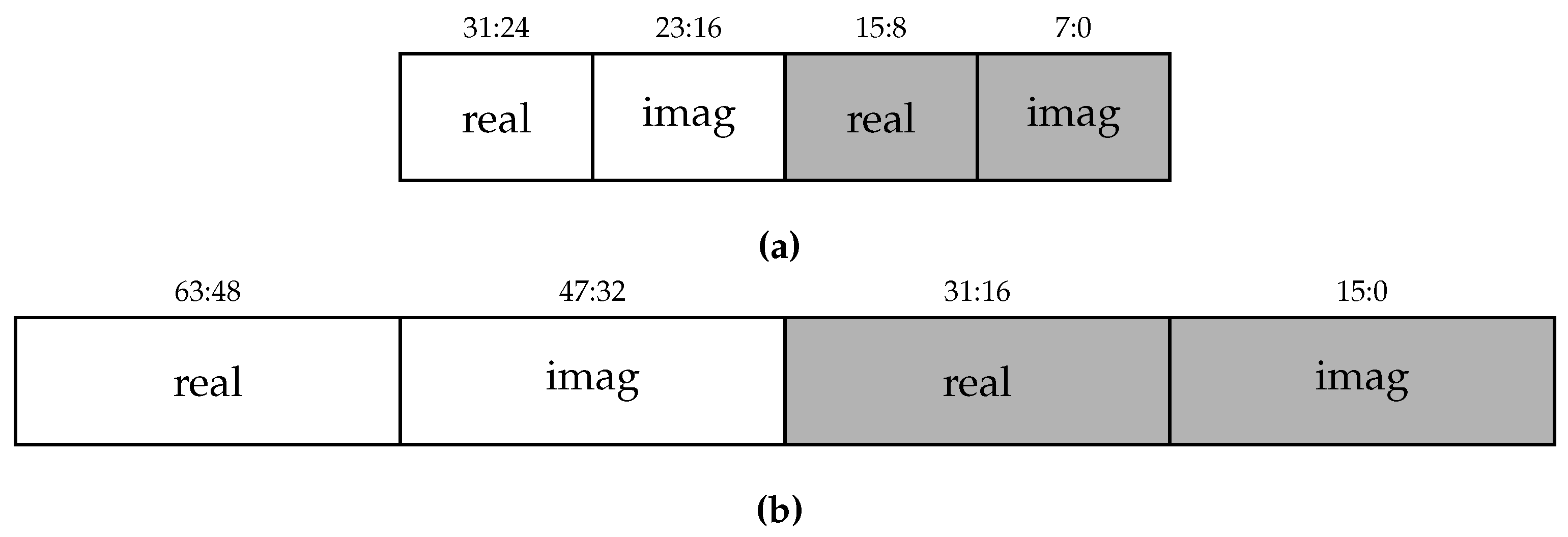
Each address corresponds to a memory word, which stores two FFT points as illustrated in
Figure 1; one point in the left (white) half and the other in the right (gray) half. The tuple
represents the position of the data point in the memory. The coordinate
a is the memory address and the coordinate
f specifies in which half of the memory word the element resides. Each data point, in
Figure 2 is identified by an index
x that was assigned to it after the application of the bit-reversal permutation. The idea behind the permutations is to have stored in a single memory word each butterfly pair of the upcoming stage.
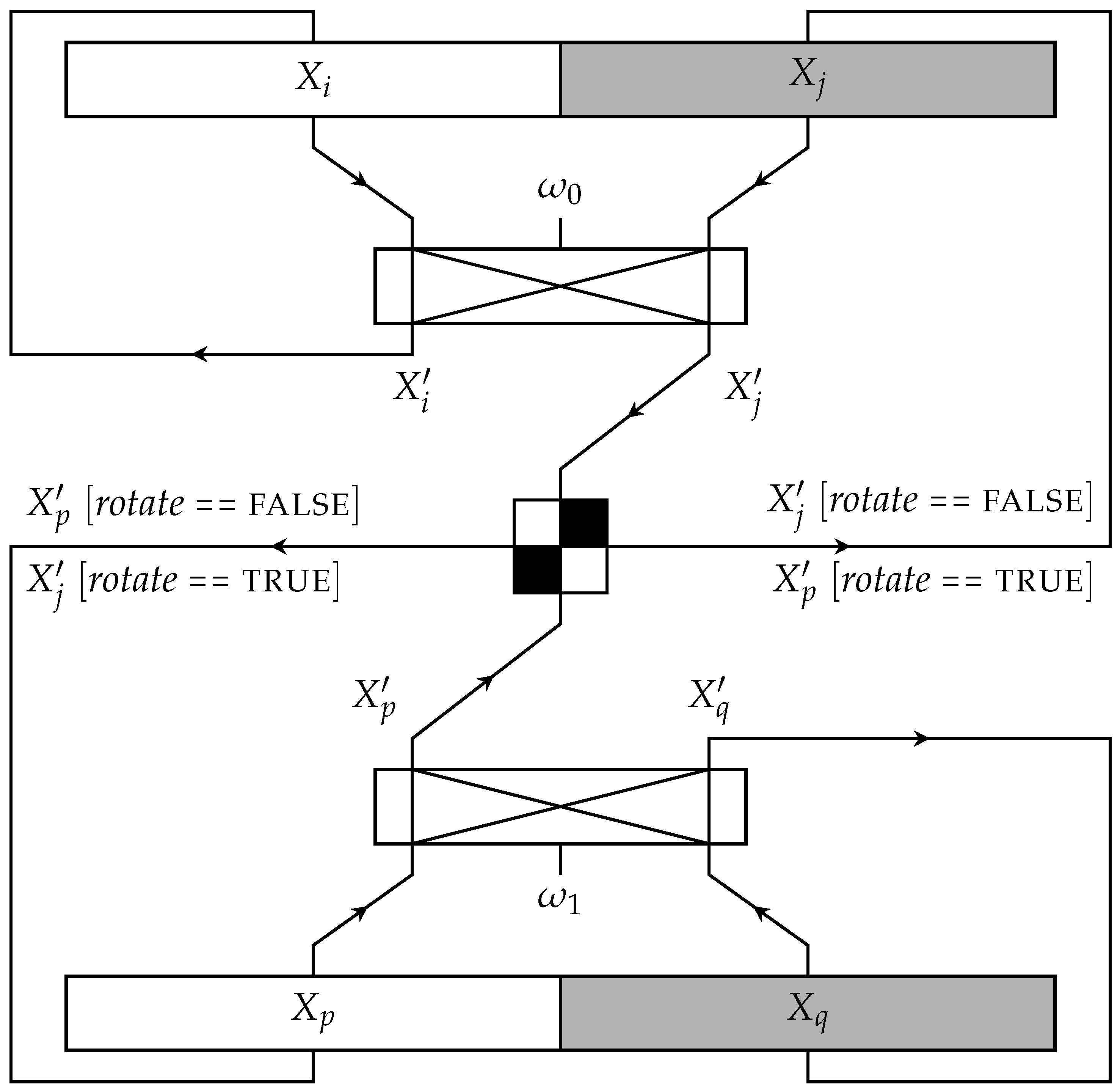
The term
main operation (
Figure 3) for this paper denotes the following commands. First, the CPU loads the two memory words in its registers, e.g., the first word contains the FFT couple
and
and the second word
and
. Second, the CPU completes the two butterfly computations: first, on the couple
and
and at the next butterfly cycle on the couple
and
. Third, it exchanges
and
to prepare the couples for the following stage’s butterfly computations and stores these words back in the memory.
Figure 2 depicts the permutation and denotes the respective exchange by using different quadrant colors in the circle, which represents the butterfly computations.
Figure 2 shows the Signal Flow Graph (SFG) of the in-place FFT and the indexes of the two data at each memory address at each stage. The circle’s separation in quadrants denotes the following:
The upper two quadrants refer to the first butterfly operation, while the lower two quadrants refer to the second. In addition, each of the four quadrants corresponds to each of the four data points loaded every time.
Black quadrants imply that the corresponding data points are exchanged, while the white quadrants denote no data exchange.
The number in the white quadrants indicates the power at which the stage’s corresponding principal root of unity is raised.
For each input data point, we use the notation , where its index stands for the position of the corresponding data point on the data stream after the bit-reversal permutation has been performed. Thus, the subscript never changes and the result produced by the i-th stage is denoted with additional prime (′) symbols.
A formal proof that the proposed permutations produce a correct FFT is in
Appendix A along with an eight-point input FFT example in
Appendix B.
| Listing 1. MainOp procedure. |
| MainOp |
| 1 |
| 2 |
| 3 Butterfly |
| 4 |
| 5 |
| 6 Butterfly |
| 7 if rotate == false |
| 8 |
| 9 |
| 10 else |
| 11 |
| 12 |
3.2. Pseudocode
Listing 3 presents the pseudocode. Line 1 calculates the
X array’s size. The for loop at line 2 runs once per FFT stage apart from the last stage, which differs with respect to the generation of twiddle factors and the permutation. Lines 2 to 15 represent all the stages but the last. Lines 16 to 22 represent the last. First, we analyze the lines 2 to 15. The while loop in lines 6 to 15 executes the butterfly calculations of the
i-th stage and generates the twiddle factor for each of them. The
main operation is implemented by the
MainOp procedure; this is invoked in every iteration. It loads memory words from the addresses
j and
,
, and it computes the two respective butterflies. Both butterflies use the same twiddle factor, which equals
. When the technique completes
iterations, both
k and
reset to their initial values and
j increases by
. Finally, the line 23 transforms the array to be read (output) in the column’s major order, while maintaining its size and providing the output data in the standard order.
Figure 4 depicts the Data Flow Graph (DFG) of the pseudocode presented in Listing 3.
| Listing 2. Butterfly procedure. |
| Butterfly |
| 1 |
| 2 |
| 3 |
| 4 return |
3.3. Data and Number Representation
A single memory address stores two data which are either FFT input points or intermediate or final results. Each of these data has a real and an imaginary number. This work uses for each number either an FP or a BFP representation. The following two paragraphs describe these two representations. Note here that the proposed implementations in the AVR32 and the Myriad 2 use only 8-bit numbers (16-bit complex numbers), in the Raspberry Pi Zero 2W only 16-bit numbers (32-bit complex numbers) and in the FPGA both 8-bit and 16-bit numbers.
3.3.1. Floating Points
A binary FP number consists of the sign bit, the exponent bits
and the significand bits
. Since the FP8 numbers are not yet standardized, researchers utilize the available 8 bits differently [
11,
12]. The format
characterizes the FP8 numbers, based on the length of each field. This work adopts the (1.4.3) format because it provides wider numeric range than the formats with smaller exponent field and better precision that the formats with smaller significand field [
12,
24]. Following the Institute of Electrical and Electronics Engineers’ (IEEE) 754 standard [
25], the exponent bias calculation follows the formula
, where
N is the number of bits in the exponent field. Consequently, the exponent bias for the
format is set to seven.
| Listing 3. FFT procedure. |
| FFT(X) |
| 1 |
| 2 for to |
| 3 |
| 4 |
| 5 |
| 6 while |
7 MainOp
true) |
| 8 |
| 9 if |
| 10 |
| 11 |
| 12 else |
| 13 |
| 14 |
| 15 |
| 16 |
| 17 |
| 18 while |
| 19 |
20 MainOp
false) |
| 21 |
| 22 |
| 23 return |
The 32-bit word length AVR32 and the Intel Movidius Myriad 2 lack support for FP8 operations. To address this limitation, the process converts the numbers from single-precision floating point (FP32) to FP8 for memory storage and back to FP32 when performing arithmetic operations. Even though this conversion adds an overhead to the algorithm’s execution time, the method remains effective. The code to convert between FP8 and FP32 is publicly available in [
26], along with a detailed description of its inner workings. To convert from FP32 to FP8, the process works on each field of the FP32 number as follows:
Keep the sign bit unchanged.
Convert large or infinity FP32 exponents to infinity in FP8, as they cannot fit within its limited numeric range. Similarly, convert small or subnormal FP32 exponents to zero in FP8, due to its limited precision.
Convert intermediate values by adjusting the FP32 exponent to fit within the biased FP8 exponent and truncate the FP32 significand to three bits, applying rounding using the next least significant bit of the FP32 significand field.
Create FP8 subnormal values following the IEEE 754 standard [
25] rules.
Similarly, the process converts the numbers between FP16 and FP32 on 64-bit word processors like the Raspberry Pi Zero 2W. The FP16 numbers, being standardized, use the
format [
25] and allow the native conversion to and from the FP32 format on the supported hardware [
27].
Figure 4.
The Data Flow Graph (DFG) of Listing 3. The graph follows the notation summarized in [
28]: any circular node represents an operation to be applied on its input, checking if it satisfies the corresponding inequality; the wide, white rectangles are DFGs that apply the
MainOp procedure to all the data points they receive and subsequently increment the stage variable; the gating structures are drawn with light gray color and expect an event signal to deliver the values from their input ports to their output ports; the diamond-shaped deciding actor generates an event signal on its T(rue) arm or F(alse) arm, based on the boolean input it receives.
3.3.2. Block Floating Points
A BFP number comprises the mantissa
m and the scaling factor or exponent
e. It is defined as a tuple of
and its value is
. The binary fixed-point format represents both the mantissa and the scaling factor as signed integers. All BFPs in a block
B share the same scaling factor, making the BFP architecture efficient with respect to memory usage and of higher dynamic range than the FP numbers with the same number of bits [
29]. The mantissa is normalized (this contrasts with prior work on BFPs, which assumes that at least one of the block’s mantissas is greater than or equal to one [
29,
30,
31]) in the interval
, so that there is at least one mantissa
m (in the block) for which
. Therefore, a fixed-point, two’s complement, number with at least two integer bits may represent the mantissa. The scaling factor is available only when all the data points in the block have been processed [
30] and the scaling factor is computed according to the normalization criteria. Certain bits of the mantissa’s Most Significant Bits (MSBs) act as
guard bits to prevent overflows before normalization. In the case of butterfly operations that receive normalized BFPs in the input, a single
guard bit suffices to prevent overflows in the output [
32,
33,
34].
The BFP number representation has a key role in the proposed method for storing the FFT input points and the intermediate results in the memory as 8-bit (in the AVR32, Myriad 2) and 16-bit (in the Raspberry Pi Zero 2W). Note that during the butterfly calculations in the above processors (all these units operate with 32 bits) these lengths are augmented to 32 bit in all cases. The 8-bit BFP and 16-bit BFP are tailored to be stored in the memory and use two integer bits. In the processors the augmented representation (32 bits) is able to prevent overflows and retain precision by employing 32-bit mantissas (32-bit block floating-point, BFP32) with three integer bits. This additional integer bit acts as the guard bit (the memory number representations do not include a guard bit). All the data use mantissas with the two’s complement representation of signed numbers. The BFP representations both in the memory and in the processor share the same scaling factor, which is initially zero. The conversion steps between the memory and the processor representations in all stages are the following:
Retrieve mantissas (8-bit or 16-bit) from memory and convert them to the augmented 32-bit representation;
Normalize the 32-bit mantissas and update the block’s scaling factor, respectively;
Perform calculations on the 32-bit mantissas;
Round the 32-bit mantissas and perform the overflow management to form the memory-tailored mantissas (8-bit or 16-bit) and store them back in memory.
3.4. Processing Devices and Platforms
The following paragraphs describe the specifics of the processors and the corresponding development platforms chosen to execute the in-place FFT code.
3.4.1. Atmel AVR32 Microcontroller
The first device for validation is the space-proven GomSpace NanoMind A3200 OBC [
35]. This system includes the Atmel AVR32 (AT32UC3C0512C) microcontroller unit (MCU) [
13], an uncached 32-bit Reduced Instruction Set Computer (RISC) architecture featuring a floating point unit (FPU), compliant with the IEEE 754 FP standard [
25]. The AVR32 MCU operates at 66 MHz, with 64 kB Static Random-Access Memory (SRAM) and 512 kB of build-in flash memory. Both the FP8 and the BFP8 implementations undergo evaluation on the NanoMind A3200 board, using its Software Development Kit (SDK). The algorithm runs on top of the FreeRTOS [
36] real-time operating system (RTOS), alongside other CubeSat Housekeeping tasks, to simulate a real-world operational scenario.
3.4.2. Movidius Myriad 2 Accelerator
The Intel Movidius Myriad 2 (MA2450) processing unit [
16] serves as a space-proven computing device, with a role closer to an image/vision-processing accelerator, as in the HPCB project [
17], rather than a CubeSat controller. It also operates as an edge device, especially for camera-based applications with low power requirements. It has a clock frequency of 180 MHz. The current implementation uses one 32-bit LEON processor to initialize the Real-Time Executive for Multiprocessor Systems (RTEMS) RTOS [
37], a 32-bit Streaming Hybrid Architecture Vector Engine (SHAVE) core for the FFT calculations and a shared SRAM memory between the LEON processor and the SHAVE core for the data element storage. Two applications test both the FP8 and the BFP8 memory configurations.
Section 3.3.1 and
Section 3.3.2 describe these configurations using uncached memory accesses. These applications undergo evaluation using the Myriad Development Kit (MDK) provided by the board manufacturer.
3.4.3. Raspberry Pi Zero 2W
The Raspberry Pi Zero 2W [
18] features the quad-core 64-bit ARM Cortex-A53 processor clocked at 1 GHz. Its low cost and general availability make it well suited for edge computing applications. Its 64-bit word accommodates two FFT data points with each consisting of a real and an imaginary part and thereby storing four 16-bit arithmetic values. The ARM processor supports native conversion between FP16 and FP32 [
27]. Both the FP16 and the BFP16 implementations run on top of the Debian-based Linux operating system (OS) [
38].
3.4.4. The Zynq 7000 FPGA Accelerator Design
For the sake of comparison of the execution time and the power consumption of the processors [
13,
16,
18] to a hardware accelerator, the proposed technique is implemented on the XC7Z007S FPGA [
20] of the Zynq 7000 SoC family [
39]. The accelerator was tested on the Digilent board Cora Z7S [
40] with two variants. The first variant has the same 32-bit memory word length as the space-grade devices [
13,
16] in this work, where data are 8-bit binaries. The second uses 16-bit data and it was designed to evaluate the difference. Apart from this difference, both schemes involve a single radix-2 butterfly computing circuit, which maps the pseudocode of
Section 3.2 onto the FPGA resources.
BFPs with 8- and 16-bit mantissas represent the FFT data points for the two variants, respectively. For both variants, the two (2) MSBs of the BFP’s mantissa represent the integral part and the remaining Least Significant Bits (LSBs) represent the fractional part. Internal circuits of the butterfly processor resize the BFPs to account for possible overflows, while others round and truncate the results, to fit in the appropriate 8- or 16-bit memory format of the variant. A Read-Only Memory (ROM) stores twiddle factors for an n-point FFT that correspond to half the n-th roots of unity. The circuit produces the other half by computing the negative values of the already stored. At the FFT completion, the system contains in memory the normalized FFT results. It will also provide as output the number of shifts performed throughout the stages.
4. Results
The current section presents the results of the execution of the Listing 3 code on the AVR32, Myriad 2, Raspberry Pi Zero 2W and the Xilinx Zynq 7000 XC7Z007S FPGA. These results include the SNR, execution times and the power consumption for all devices. We note here that for AVR32, Myriad 2 and Raspberry Pi Zero 2W, the number of experiments is 10000 to ensure reliability, while for the FPGA it is 1000 due to time needed for testing on the FPGA. Moreover, to show the applicability of the method, the section includes execution on computationally more powerful devices. Furthermore, it describes the criteria for comparing the proposed method with alternative approaches.
4.1. Execution on Space-Proven Processors
Both AVR32 and Myriad 2 have 32-bit word lengths. They store two data (complex numbers) in each word, and thereby each memory word stores four 8-bit arithmetic values.
Table 2 presents the timing summary using BFPs with 8-bit (2 integer bits and 6 fractional bits) mantissa (BFP8) and FP8 data types. In both devices, the BFP8 implementation improved execution time compared to the corresponding one of the FP8. The main difference between the two implementations is that the BFP8 implementation performs the FFT calculations by using the Arithmetic Logic Unit (ALU) of the processor, whereas the FP8 performs the calculations by using the FPU.
4.2. Execution on Edge Processors
The Raspberry Pi Zero 2W edge device uses a 64-bit word length for the two FFT data and so each memory word stores four 16-bit arithmetic values.
Table 3 presents the timing summary using BFPs with 16-bit (2 integer bits and 14 fractional bits) mantissa (BFP16) and FP16 data types. The FP16 implementation has a shorter execution time compared to that of the BFP16. Note here that the Raspberry Pi Zero 2W supports native conversions between the FP16 and FP32 formats [
27].
Regarding the Zynq 7000 XC7Z007S FPGA implementation,
Table 4 presents the results of the Vivado tool [
41] for the 8-bit and 16-bit architectures for the range of 1K to 16K FFT input points. The third column gives the percentage of the resource utilization of the FPGA and the fourth the estimated power. The fifth column presents the total execution time. As expected, the execution time follows almost linearly the increase in the FFT input size. The clock frequency for all the designs is 100 MHz. The 16-bit architecture uses an average of 30% more resources than the 8-bit architecture and therefore consumes on average 12% more power.
The major resource-utilization consideration relates to Look-Up Tables (LUTs) and Block RAMs (BRAMs), which scale proportionally with the bit-level input size of the problem. The resources completing the architecture are the Flip-Flops (FFs), with usage percentage of 2.8% for the 32-bit word and 3.7% for the 64-bit word architectures, respectively. Finally, the Butterfly Operation Core within the design uses four multipliers. These multipliers are pipelined multiplication units from the Digital Signal Processing (DSP) Slices available in the programmable fabric. All the designs use these four DSP multipliers.
4.3. Signal-to-Noise Ratio
The input simulation evaluates the signal-processing quality of the proposed technique by employing a methodology similar that presented in [
30,
31], where each input data point constitutes the output of a simulated 32-bit sensor. The values of the input sequence follow the uniform distribution in the interval
and the measurement of the processing quality is the SNR metric defined as:
where
is a 64-bit double precision FP output sequence and
is an output computed with one of the data representations described in
Section 3.3.
Table 5 presents the results for the entire range of FFT input points used in the evaluation experiments. Each output is compared to the corresponding results of executing the FFT
numpy Python library [
42], which uses double precision numbers. The FPGA implementation uses only the BFP representation, and for this,
Table 5 lists the FPGA results separately in the last two columns. The results represent the mean value produced by the execution of 1000 experiments.
4.4. Power Consumption
In order to determine the average power consumption of all the devices, this work employed both the measurement-based energy-profiling and the simulator-based energy-estimation methods [
43]. For the AVR32 and Raspberry Pi Zero 2W, the power results came from instrument-based measurements using the ChargerLAB POWER-Z KM003C. The Myriad’s MDK provides profiling tools to estimate the average power consumption through simulation.
Table 6 presents the results of the power consumption with the space-proven devices exhibiting lower average power consumption compared to the edge Zero 2W. The Myriad 2 VPU accelerator demonstrates significantly lower power consumption than the processors of the AVR32 and the Raspberry Pi Zero 2W.
A notable result is that all the floating point implementations exhibit slightly lower average power consumption compared to the block floating point implementations. In the case of AVR32, the difference accounts for approximately 0.1% of its maximum power consumption [
35] and it is even smaller for the Myriad 2 and Raspberry Pi Zero 2W. Actually, the power consumption of a single butterfly operation is less than that of the same butterfly with floating point numbers in all the above devices. The difference of the BFP power consumption comes from (a) the operations required to prepare the BFP block (
Section 3.3.2) by normalizing all the FFT data for the butterfly computations of that stage and (b) the operations before storing back the entire BFP block. The most detailed case is that of Myriad 2, which was investigated and analyzed using its officially provided simulator that enables precise power measurements. Using this tool, the power consumption of a single butterfly operation on Myriad 2 measures 26.52152 mW with the BFP8 and 26.55837 mW with the FP8; and the slight increase in average power consumption during the full FFT execution comes from the preparations for loading and storing the data of the BFP blocks (one block per stage).
We note here that although the total power consumption does vary with input size due to its dependence on execution time, in this work we focus on the average power consumption, which remains constant. This is because average power reflects the rate of energy usage over time, which is influenced more by the hardware’s operational characteristics than by the input size itself.
4.5. Execution on Devices of Higher Computational Power
Although the proposed method targets the efficiency of single-memory-bank processors, the current section shows results from executions of the method on processors equipped with Graphics Processing Units (GPUs) and more powerful FGPAs of the Xilinx Zynq family to emphasize its general applicability.
First is the Xilinx Zynq Z-7045 (Advanced Micro Devices, California, USA), chosen because it is the FPGA dedicated to the image-compression task for the ERMIS 3 mission. The proposed method on this FPGA was executed at 100 MHz, the same clock frequency as with the smaller Zynq 7000 XC7Z007S (Advanced Micro Devices, California, USA). As expected, it produces almost the same timing results shown in
Table 7. That is 0.05s for the 1K point input and 32-bit word length, up to 1.14 s for the 16 K point input and 64-bit word length. Apart from the lower utilization metrics (Z-7045 FPGA is significantly larger with respect to resources than CX7Z007S),
Table 7 reports the power consumption, which is increased slightly mainly due to the larger idle power consumption on the Z-7045 chip.
Computing devices equipped with GPUs can also execute the proposed method, although there are FFT techniques optimized for the GPU hardware with respect to execution times. The Nvidia RTX 3080 (NVIDIA, Santa Clara, CA, USA) with 10 GB RAM is a powerful GPU and can execute the proposed method. Another device carrying GPU is the NVIDIA Jetson Nano and the entire design is accomplished with the Developer Kit that includes the TX1 Module [
44]. The latter is a low-power, high-performance edge computing device featuring a quad-core ARM Cortex-A57 CPU (ARM Holdings, Cambridge, UK) and a 256-core NVIDIA Maxwell GPU (NVIDIA, California, USA). The system includes 4 GB of LPDDR4 unified memory with a 64-bit word length, enabling storage of two FFT data points, consisting of four 16-bit arithmetic values. Both FP16 and BFP16 implementations were developed on the officially supported Debian-based OS and leverage the on-board GPU for executing the FFT algorithm. The execution results are gathered in the
Table 8.
4.6. Comparison Criteria
The above executions of the proposed method on the sample space-proven and edge computing devices show the performance efficiency on devices with limited resources. Consequently, the comparison to other in-place techniques or to the classical out-of-place approaches will take into account all the features that contribute to the efficiency.
The first in significance are the memory requirements for each technique. This is central because it gives the upper bound of the FFT input size that each processing device will be able to complete. The second criterion, equally important as the first, is the achievable SNR by each technique. Moreover, the combination of the latter two shows whether the proposed method can successfully support the FFT calculations specified for each application.
Power consumption is the third benchmark that characterizes each technique and the resulting mean values have to meet the device’s specifications. The actual mean power is for the devices that were tested and measured on the bench. For the development tool-based power calculation, the engineers have to consider whether the actual mean value can be greater because of the device’s power waste as heat.
Another criterion is how each technique exploits the computing resources of a device. The FP and BFP number representations use different parts of the processor. Hence, they show a different performance on various devices, which depends on the device’s processor architecture.
Time efficiency also characterizes each implementation. There are two time characteristics quite different from each other that we consider here: the time required for the execution of each FFT implementation and the time needed by the designing group to develop the implementation. First, the execution time is the typical characteristic of each implementation. However, given that the arithmetic unit executing the FFT has a constant throughput, e.g., a butterfly pair per cycle, the proposed in-place method can improve the total execution time in the cases of a slower memory access time with respect to the arithmetic unit processing time. The time needed for the development of each FFT implementation grades each approach. The following section analyzes the performance of the proposed method based on the above criteria.
5. Discussion
The main design advantages of the proposed method are first the design of a simple addressing scheme adopting a straightforward permutation and second the efficient use of the BFP representation. The addressing scheme is the same for all the butterflies and stages, tailored for a single memory bank CPU architecture of COTS processors. The following paragraphs discuss the gains of the method regarding resource utilization, then of the FP and BFP performance and the trade-offs of the FP and BFP configurations and they conclude by focusing on the benefits of using the proposed method in future applications.
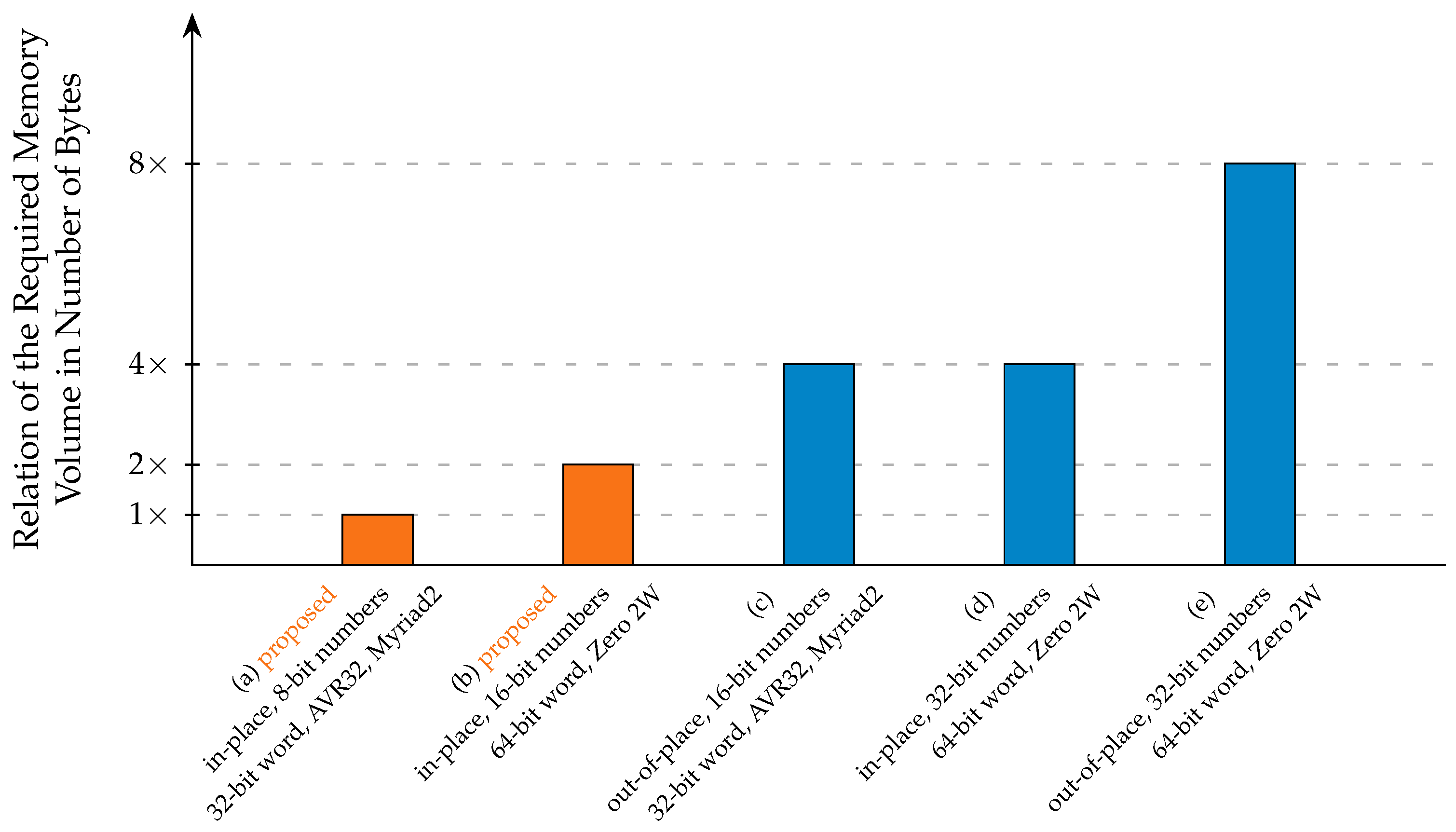
The proposed method allows processors with limited resources to handle a large number of FFT input points and at the same time leave sufficient memory space for other edge applications or CubeSat mission-specific tasks. This is due to the efficient number configuration, which reduces the number of bits to achieve the dual FFT data in each address while the SNR remains the same. The advantage of the 8-bit number representation is the significant improvement in memory utilization (a) by a factor of two compared to the corresponding of 16-bit, (b) by a factor of four with respect to in-place techniques using 32-bit number representation and finally (c) by a factor of eight compared to the out-of-place techniques using 32-bit number representation. For example, the memory utilization of this in-place FFT allows the AVR32 to process up to 16K FFT points, which is sufficient for space applications [
45,
46]. Then, the remaining AVR32’s 32 kB memory allows the processor to perform additional functions, such as housekeeping and managing peripheral devices along with the FFT process. Comparison to significant FFT implementations also show the advantages of the proposed method. Among the FFT libraries, the noteworthy FFTW [
47] supports only floating point data types: float (32 bits), double (64 bits) and long double (128 bits). Even when configured for its most memory-efficient mode (in-place computation using 32-bit floating point numbers), FFTW requires approximately four times the memory capacity needed by the 8-bit version of the proposed method. Furthermore, it exhibits about twice the memory consumption compared to the 16-bit version of the proposed method. Notably, the proposed method also supports block floating point numbers, contributing to a better SNR while maintaining low memory usage.
Figure 5 illustrates the comparison of the required memory volume, as a number of bytes, between the proposed in-place method and alternative FFT techniques. All the techniques refer to the same number of input FFT points (data) represented either as FP or BFP complex numbers (data). We note here that any out-of-place technique requires double memory volume compared to the corresponding in-place using the same data bit width considering the same computing device. The orange columns show the required number of bytes by the proposed method on the AVR32 and Myriad 2 (a) and on the Zero 2W (b). The alternative techniques are in the blue columns and they all store one complex number (single data) in each address. The blue column (c) shows the required memory for the out-of-place execution on the AVR32 and Myriad 2. These executions were completed in our lab only to verify resource utilization along with the results presented in
Section 4. The blue column (d) shows the required memory by an in-place method, which uses a 64-bit wide memory, developed in our laboratory and similar to [
48]. The (e) blue column shows the required memory in the straightforward FFT out-of-place case, which was also executed in our laboratory and requires double the size of memory of the (d) in-place case.
This work focused mainly on improving the combination of SNR results and in-place organization for processors with limited resources. The experimental results of the SNR are summarized in
Table 5. In all experiments, the BFP data types lead to significantly better SNR results, compared to the FP data types. For this reason, the research team has considered for future development mainly the BFP executions; therefore, the comparison of the execution times focuses only on the BFP results. In this work, the BFP8 data type allocates 6 bits to the fractional part, whereas the FP8
format data type uses 3 bits. Similarly, the BFP16 data type allocates 14 bits for the fractional part, compared to 10 bits in the FP16 data type. As expected, increasing the bit number in the fractional part enhances the accuracy of the results. The proposed in-place method achieves better execution time by using BFP8 data types on the 32-bit space-grade processors and BFP16 data types on the 64-bit Raspberry Pi Zero 2W than the out-of-place FFT implementation with BFP32 data types.
Table 9 presents the execution times of the proposed in-place technique and the out-of-place FFT technique.
Figure 6 depicts the SNR levels for the BFP representation with 8-bit data types (
for BFP8) and the improved ones with 16-bit data types (
dB for BFP16). The application developers can opt for the most suitable hardware and data type according to the requirements of the target application. Considering the twiddle factors, as mentioned in
Section 3, the FPGA design stores these in a ROM while the CPU implementations store the principal root of unity corresponding to each stage and generate the twiddle factors at runtime.
Table 5 shows that the absolute difference in SNR (dB) between the FPGA and the CPU implementations is less than
when using BFP8 or BFP16 number representations. Therefore, the twiddle generation method is more efficient with respect to memory resources and it achieves results comparable to the twiddle storage method. This renders it more suitable for memory-constrained space and edge computing applications. Another advantage of the BFP representation is that it can be utilized in processing devices that do not include FPU. The normalization range for the BFP representation aligns with the input data’s and twiddle factors’ range of
. All the reported techniques in the literature, in order to enforce the state of the art normalization criteria, introduce a redundant round of normalization before stage 0, an operation that the proposed approach avoids. The omission of the guard bit in data stored in the memory enables the inclusion of an additional fractional bit. The alternative approach specifies the guard bit present and the least significant fractional bit omitted. Using the latter alternative approach in the same experimental setup, the results demonstrated that the proposed approach is over 5 dB enhanced in terms of SNR.
Considering the FP representation, for the FP8 (presented in
Section 3.3.1) the research team has selected the
format that leads to the aforementioned SNR results. This format provides an attractive solution for the balance between numerical range and precision among all the FP8 formats studied for the current application. The formats with a smaller exponent field can process a limited number of input data points because they have smaller dynamic range. Formats using a larger exponent cause the accuracy of the results to deteriorate, due to their smaller fraction field.
Finally, the memory-utilization gains improve the power consumption due to the decrease in the switching activity in the memory and also, the reduced number of load and store operations. Given the fact that only the Myriad 2 MDK provides power-consumption metrics, we note here the power consumption of the out-of-place technique in the Myriad 2, that has a 13% increase compared to this work’s in-place technique.
The BFP representation enhances the precision compared to the FP implementation, while it mitigates its limited dynamic range [
49]. In a BFP block, the exponent common to all the data requires only a single-word storage and all the bits of the BFP block data are dedicated to the mantissa (
Section 3.3.2), a fact that improves the precision. In addition, the BFP representation increments the exponent exclusively to prevent overflows and optimizes the preservation of the precision.
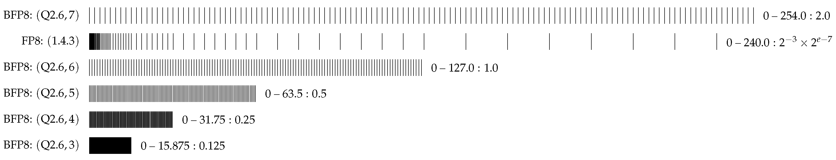
Figure 7 visualizes the proposed number representations stored in the memory of 32-bit word systems. It depicts the non-negative numbers generated by the proposed FP8 and BFP8 configurations. When the exponent remains low due to the absence of scaling to prevent overflows, the “density” of the BFP numbers is higher. Conversely, when the exponent is increased, the range of supported values expands uniformly, reducing quantization errors compared to FP8 representation. This adaptability contributes to the superior BFP8 results in
Figure 6. Consequently, the BFP configuration is tailored to the FFT application to optimize the maximum dynamic range for precision gains.
Finally, in terms of the time needed for the development of each implementation, the proposed method has a straightforward application of the code in Listing 3. Especially in a load and store architecture, the development is similar to that of any out-of-place technique, and hence the development time will be similar. This development efficiency also characterizes the scalability of the method, which can be implemented for large FFT input sizes and scales, and is most effective when the data fit within a single memory bank.
Considering the future application prospect of the proposed method, the results show that it compares favorably to the majority radix-2 in-place techniques in the literature that are based on multi-bank architectures [
5,
6,
7,
10] proposing specific circuits for addressing different groups of butterflies within each stage and different groups at each stage. This work accomplishes the data exchange in a COTS processor without spending additional clock cycles such as for prime number operations, exclusive OR calculations, etc. The second advantage is this work’s specific BFP configuration, which leads to improved SNR results in all cases. Moreover, as mentioned above, the prevailing combination of the in-place technique and the BFP SNR results will efficiently support FFT calculations in computing devices that do not include FPU. These facts make the proposed method an attractive solution for the commercially available and programmable software computing devices.


 ,
, 


