
Perovskite-Based Triboelectric Nanogenerator and Its Application Towards Self-Powered Devices


Abstract
1. Metal-Halide Perovskites
1.1. Structure and Classification of Perovskites
1.2. Properties of Perovskites
1.2.1. Strong Light Absorption Capability
1.2.2. Tunable Bandgap
1.2.3. Long Carrier Diffusion Length

2. TENG Working Principles
2.1. Four Modes of TENG
2.2. Electron Transfer Mechanism
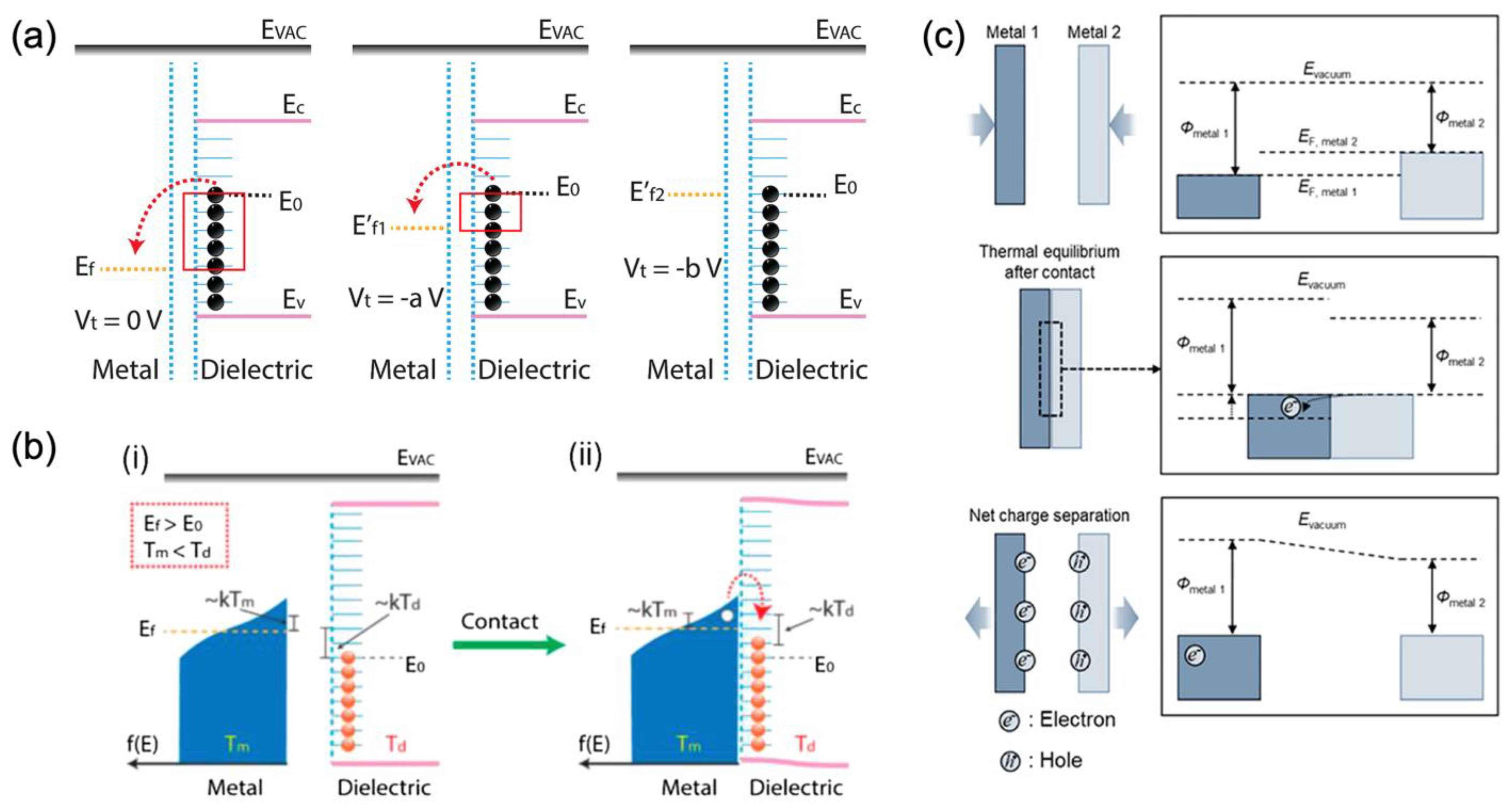
2.2.1. Metal-Dielectric and Metal-Metal
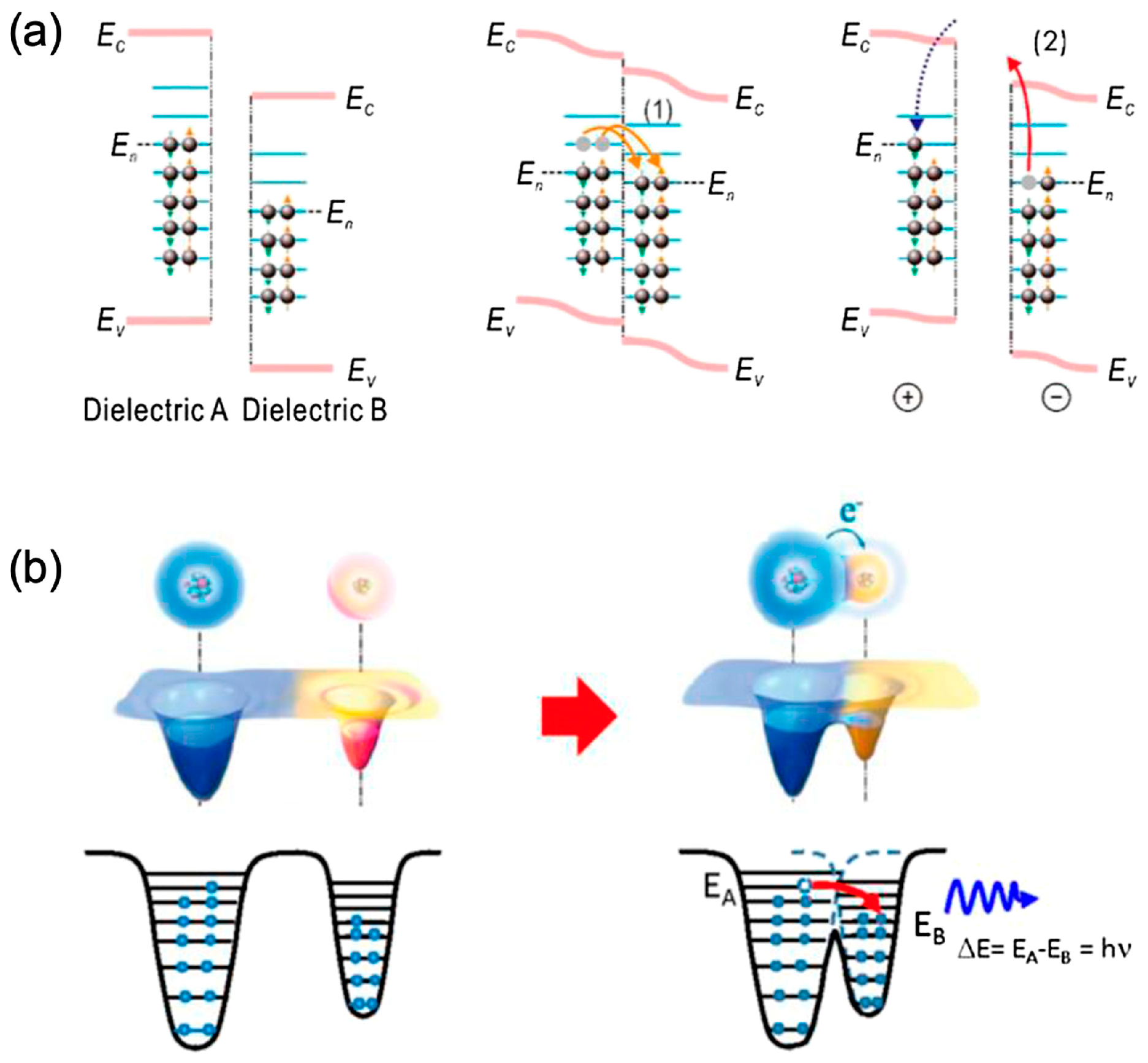
2.2.2. Dielectric-Dielectric
2.2.3. Semiconductor-Semiconductor or Semiconductor-Metal
2.3. Energy Generation Mechanism
2.3.1. AC-TENG
Fundamental Mechanism
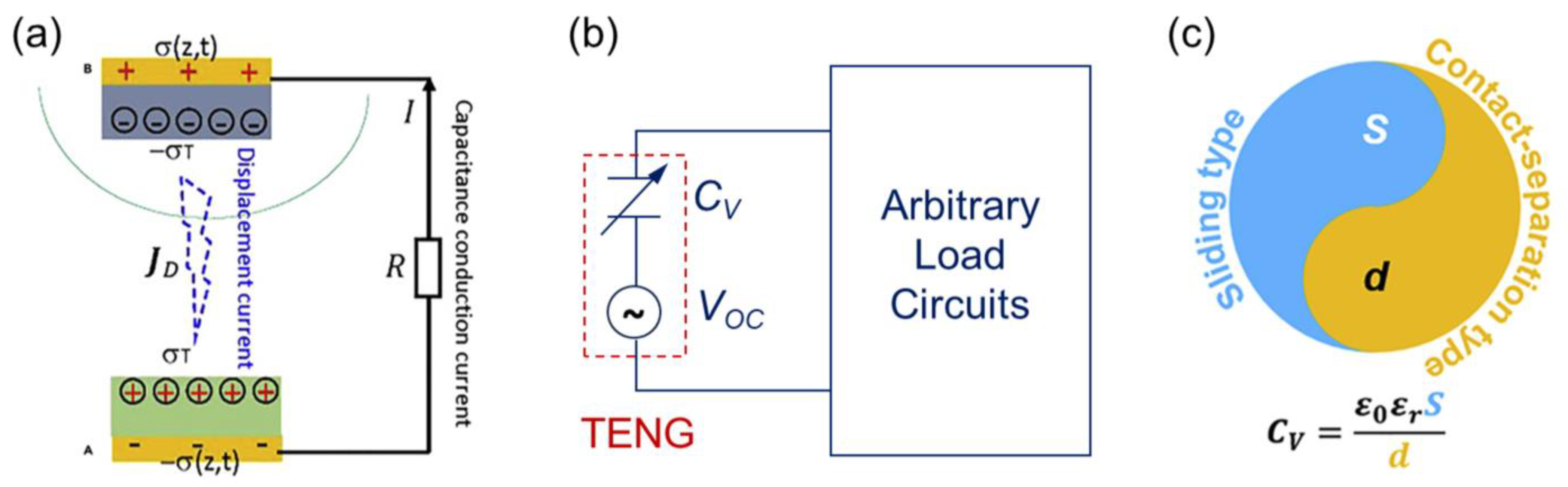
Capacitor Model
Figure of Merits
Electrostatic Breakdown
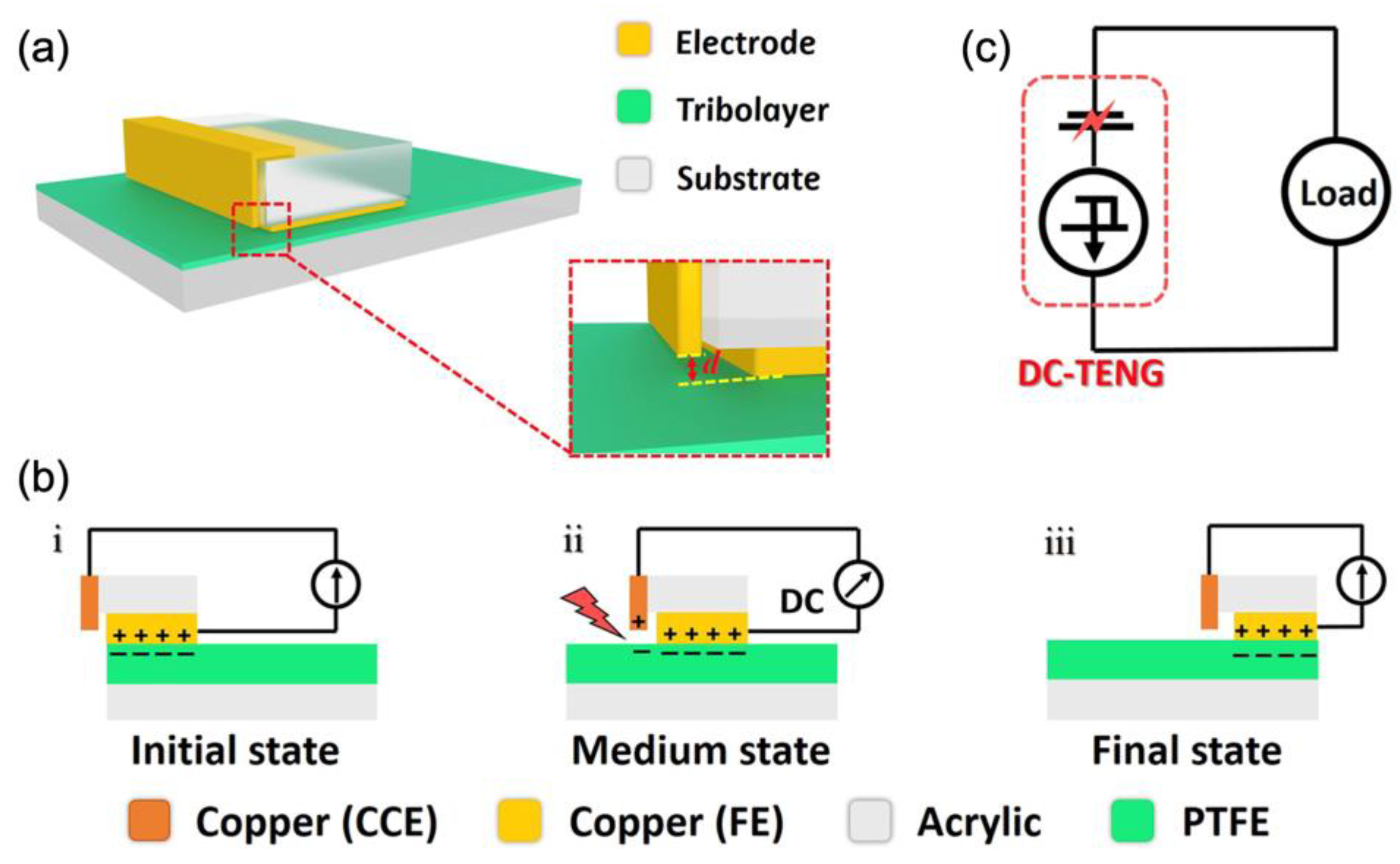
2.3.2. DC-TENG
DC-TENG Based on Non-Semiconductors
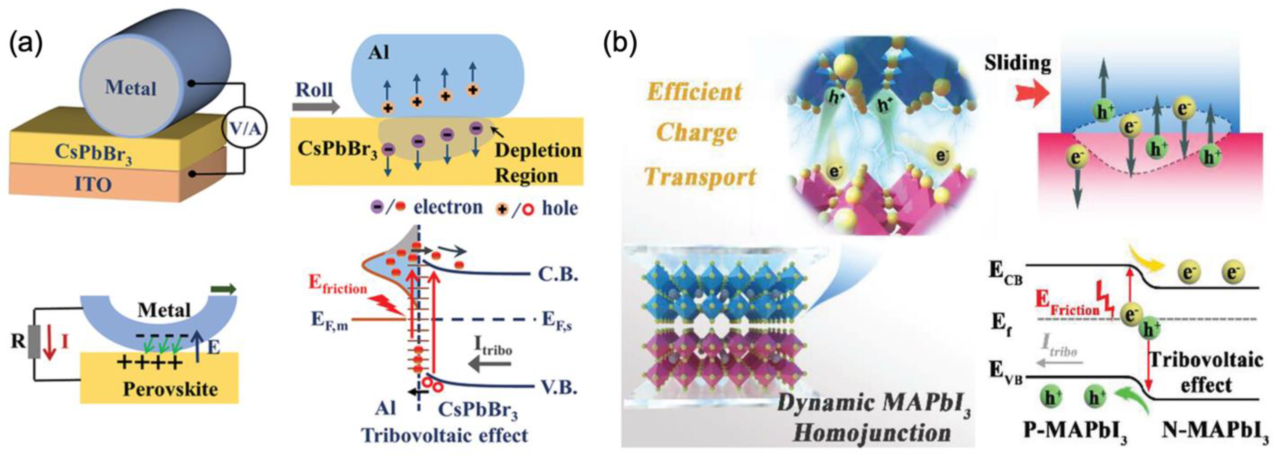
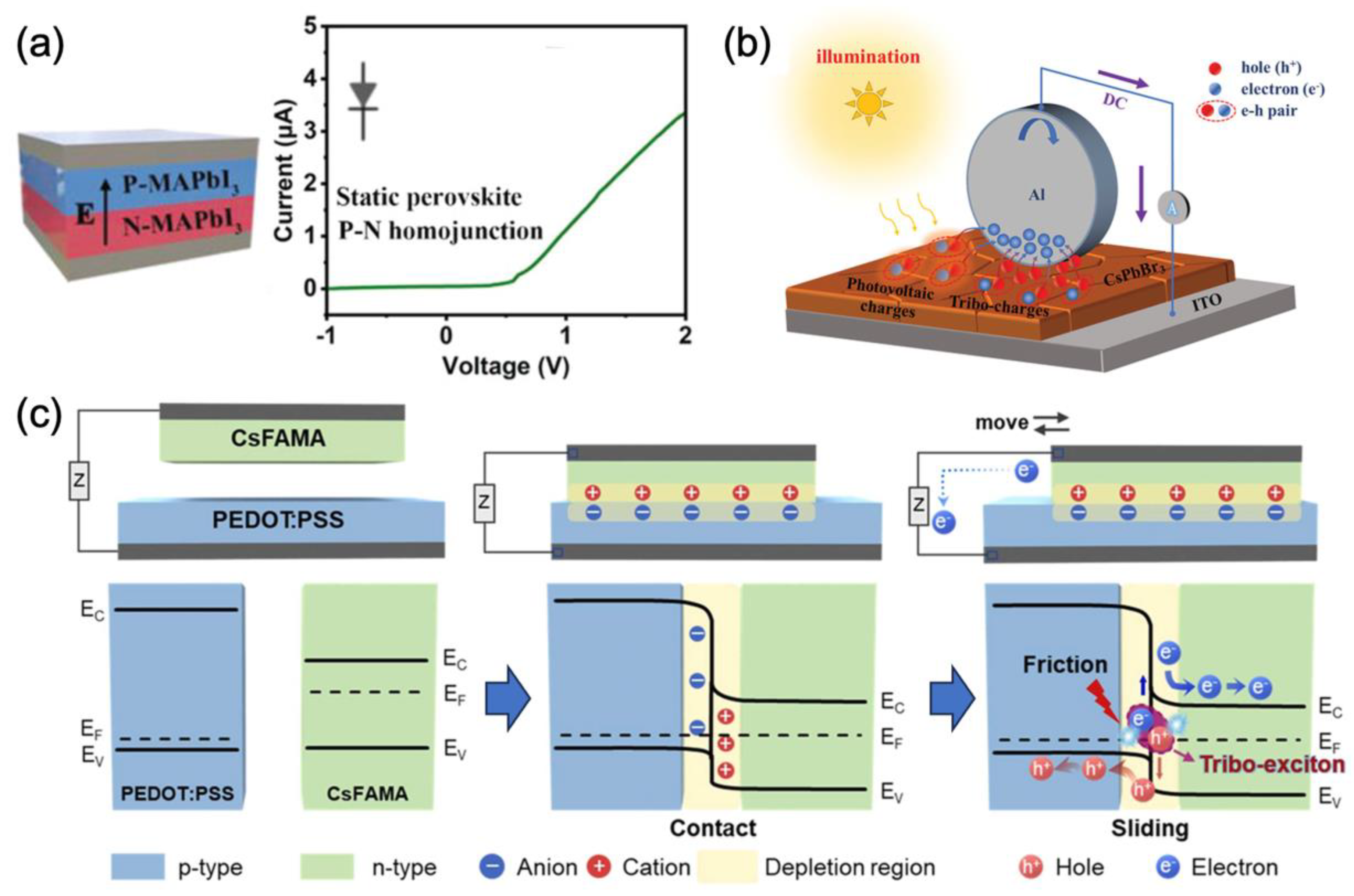
DC-TENG Based on Semiconductors
2.4. Optical Mechanisms
3. Applications
3.1. Triboelectric Nanogenerator
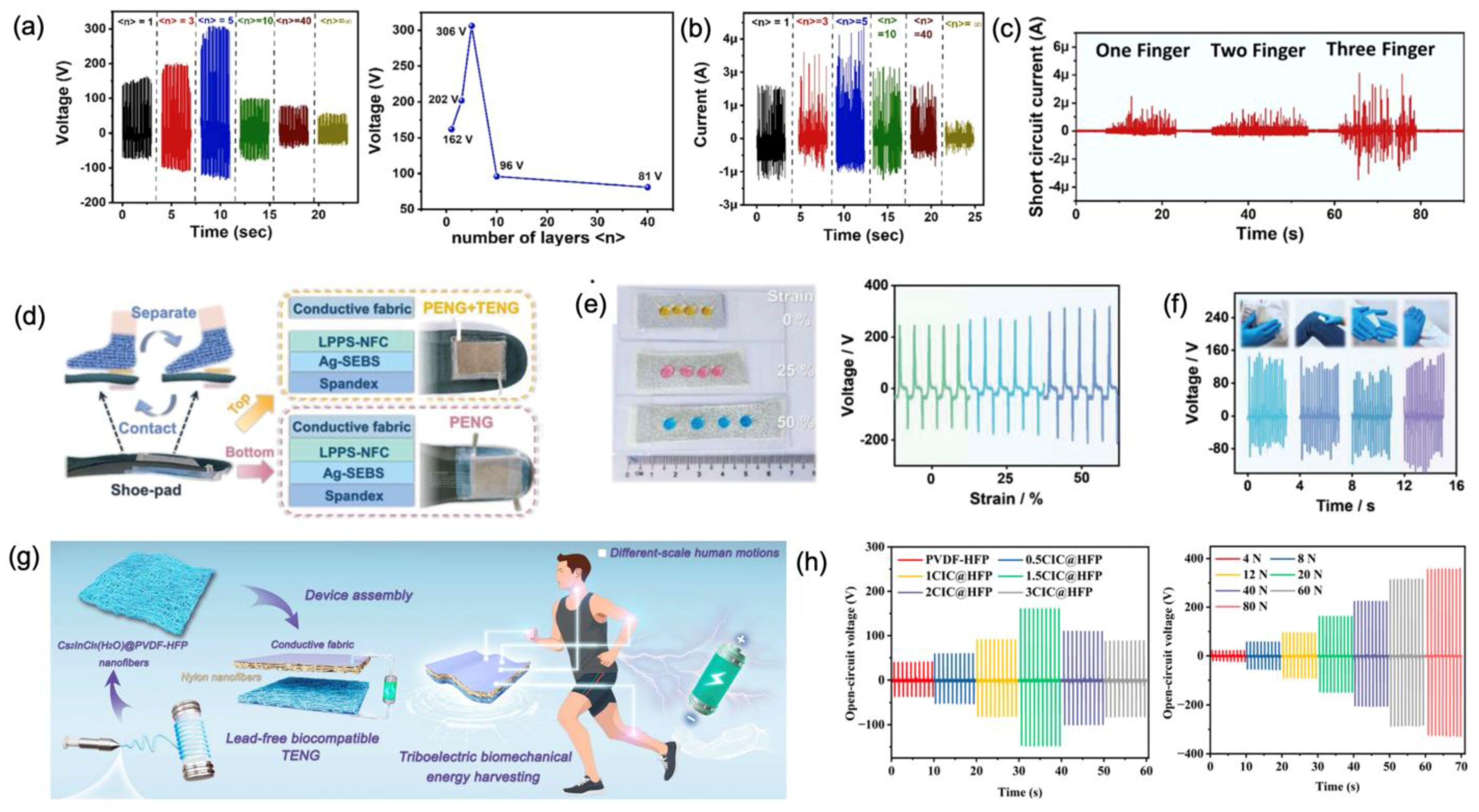
3.1.1. Energy Harvesting from Body Movements
3.1.2. Energy Harvesting from Nature
3.2. Self-Powered Sensors
3.2.1. Optical and Mechanical Dual-Mode Sensor
3.2.2. Humidity and Temperature Sensor
3.2.3. Physiology Sensor
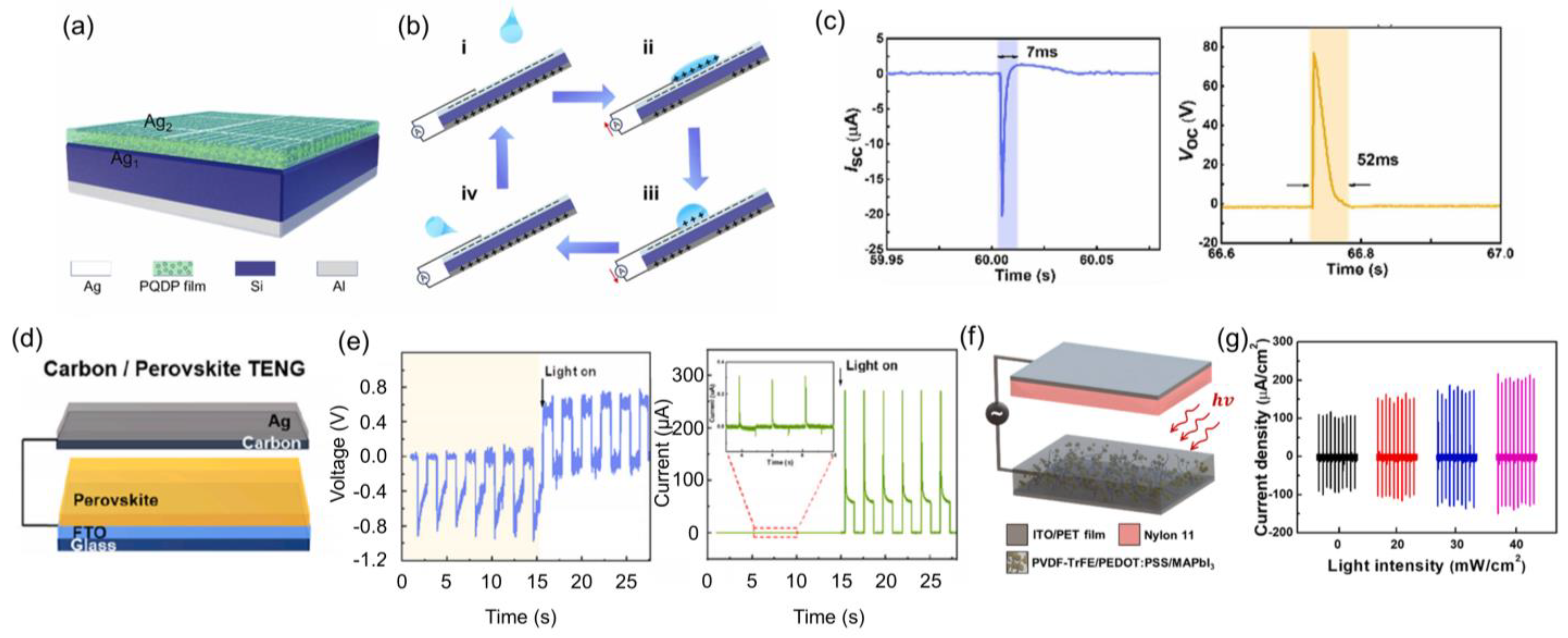
3.2.4. Triboelectric-Induced Photodetector
4. Perspectives
5. Conclusions
Author Contributions
Funding
Data Availability Statement
Conflicts of Interest
References
- Zhang, X.; Li, L.; Sun, Z.; Luo, J. Rational Chemical Doping of Metal Halide Perovskites. Chem. Soc. Rev. 2019, 48, 517–539. [Google Scholar] [CrossRef]
- Peng, J.; Chen, Y.; Zheng, K.; Pullerits, T.; Liang, Z. Insights into Charge Carrier Dynamics in Organo-Metal Halide Perovskites: From Neat Films to Solar Cells. Chem. Soc. Rev. 2017, 46, 5714–5729. [Google Scholar] [CrossRef] [PubMed]
- Kim, G.-W.; Petrozza, A. Defect Tolerance and Intolerance in Metal-Halide Perovskites. Adv. Energy Mater. 2020, 10, 2001959. [Google Scholar] [CrossRef]
- Unger, E.L.; Kegelmann, L.; Suchan, K.; Sörell, D.; Korte, L.; Albrecht, S. Roadmap and Roadblocks for the Band Gap Tunability of Metal Halide Perovskites. J. Mater. Chem. A 2017, 5, 11401–11409. [Google Scholar] [CrossRef]
- Filip, M.R.; Eperon, G.E.; Snaith, H.J.; Giustino, F. Steric Engineering of Metal-Halide Perovskites with Tunable Optical Band Gaps. Nat. Commun. 2014, 5, 5757. [Google Scholar] [CrossRef]
- Vashishtha, P.; Metin, D.Z.; Cryer, M.E.; Chen, K.; Hodgkiss, J.M.; Gaston, N.; Halpert, J.E. Shape-, Size-, and Composition-Controlled Thallium Lead Halide Perovskite Nanowires and Nanocrystals with Tunable Band Gaps. Chem. Mater. 2018, 30, 2973–2982. [Google Scholar] [CrossRef]
- Zhou, Y.; Poli, I.; Meggiolaro, D.; De Angelis, F.; Petrozza, A. Defect Activity in Metal Halide Perovskites with Wide and Narrow Bandgap. Nat. Rev. Mater. 2021, 6, 986–1002. [Google Scholar] [CrossRef]
- Gu, H.; Niu, T.; Zuo, S.; Cai, Y.; Chao, L.; Müller-Buschbaum, P.; Xia, Y.; Zhang, J.; Xing, G.; Chen, Y. Stable Metal–Halide Perovskite Colloids in Protic Ionic Liquid. CCS Chem. 2022, 4, 3264–3274. [Google Scholar] [CrossRef]
- Noel, N.K.; Wenger, B.; Habisreutinger, S.N.; Snaith, H.J. Utilizing Nonpolar Organic Solvents for the Deposition of Metal-Halide Perovskite Films and the Realization of Organic Semiconductor/Perovskite Composite Photovoltaics. ACS Energy Lett. 2022, 7, 1246–1254. [Google Scholar] [CrossRef] [PubMed]
- Du, J.; Yang, X.; Duan, J.; Wang, Y.; Tang, Q. Tailoring All-Inorganic Cesium Lead Halide Perovskites for Robust Triboelectric Nanogenerators. Nano Energy 2020, 70, 104514. [Google Scholar] [CrossRef]
- Wang, M.; Duan, J.; Yang, X.; Wang, Y.; Duan, Y.; Tang, Q. Interfacial Electric Field Enhanced Charge Density for Robust Triboelectric Nanogenerators by Tailoring Metal/Perovskite Schottky Junction. Nano Energy 2020, 73, 104747. [Google Scholar] [CrossRef]
- Kim, M.; Lee, S.; Cao, V.A.; Kim, M.C.; Nah, J. Performance Enhancement of Triboelectric Nanogenerators via Photo-Generated Carriers Using a Polymer-Perovskite Composite. Nano Energy 2023, 112, 108474. [Google Scholar] [CrossRef]
- Zhang, K.; Zhu, N.; Zhang, M.; Wang, L.; Xing, J. Opportunities and Challenges in Perovskite LED Commercialization. J. Mater. Chem. C 2021, 9, 3795–3799. [Google Scholar] [CrossRef]
- Cheng, L.; Jiang, T.; Cao, Y.; Yi, C.; Wang, N.; Huang, W.; Wang, J. Multiple-Quantum-Well Perovskites for High-Performance Light-Emitting Diodes. Adv. Mater. 2020, 32, 1904163. [Google Scholar] [CrossRef] [PubMed]
- Ma, D.; Lin, K.; Dong, Y.; Choubisa, H.; Proppe, A.H.; Wu, D.; Wang, Y.-K.; Chen, B.; Li, P.; Fan, J.Z.; et al. Distribution Control Enables Efficient Reduced-Dimensional Perovskite LEDs. Nature 2021, 599, 594–598. [Google Scholar] [CrossRef]
- Li, C.; Ma, Y.; Xiao, Y.; Shen, L.; Ding, L. Advances in Perovskite Photodetectors. InfoMat 2020, 2, 1247–1256. [Google Scholar] [CrossRef]
- Tian, W.; Zhou, H.; Li, L. Hybrid Organic–Inorganic Perovskite Photodetectors. Small 2017, 13, 1702107. [Google Scholar] [CrossRef] [PubMed]
- Miao, J.; Zhang, F. Recent Progress on Highly Sensitive Perovskite Photodetectors. J. Mater. Chem. C 2019, 7, 1741–1791. [Google Scholar] [CrossRef]
- Du, Y.; Miao, S.; Jin, Z.; Hu, Y.; Cho, Y. A Modulated Heterojunction Interface via Ferroelectric P(VDF-TrFE) towards High Performance Quasi-2D Perovskite Self-Powered Photodetectors. J. Mater. Chem. A 2024, 12, 27518–27526. [Google Scholar] [CrossRef]
- Liu, T.; Almutairi, M.M.S.; Ma, J.; Stewart, A.; Xing, Z.; Liu, M.; Hou, B.; Cho, Y. Solution-Processed Thin Film Transparent Photovoltaics: Present Challenges and Future Development. Nano-Micro Lett. 2024, 17, 49. [Google Scholar] [CrossRef]
- Li, Z.; Yang, M.; Park, J.-S.; Wei, S.-H.; Berry, J.J.; Zhu, K. Stabilizing Perovskite Structures by Tuning Tolerance Factor: Formation of Formamidinium and Cesium Lead Iodide Solid-State Alloys. Chem. Mater. 2016, 28, 284–292. [Google Scholar] [CrossRef]
- Quan, L.N.; Yuan, M.; Comin, R.; Voznyy, O.; Beauregard, E.M.; Hoogland, S.; Buin, A.; Kirmani, A.R.; Zhao, K.; Amassian, A.; et al. Ligand-Stabilized Reduced-Dimensionality Perovskites. J. Am. Chem. Soc. 2016, 138, 2649–2655. [Google Scholar] [CrossRef] [PubMed]
- Sidhik, S.; Wang, Y.; De Siena, M.; Asadpour, R.; Torma, A.J.; Terlier, T.; Ho, K.; Li, W.; Puthirath, A.B.; Shuai, X.; et al. Deterministic Fabrication of 3D/2D Perovskite Bilayer Stacks for Durable and Efficient Solar Cells. Science 2022, 377, 1425–1430. [Google Scholar] [CrossRef]
- Ding, R.; Wong, M.; Hao, J. Recent Advances in Hybrid Perovskite Nanogenerators. EcoMat 2020, 2, e12057. [Google Scholar] [CrossRef]
- Sahare, S.; Pham, H.D.; Angmo, D.; Ghoderao, P.; MacLeod, J.; Khan, S.B.; Lee, S.-L.; Singh, S.P.; Sonar, P. Emerging Perovskite Solar Cell Technology: Remedial Actions for the Foremost Challenges. Adv. Energy Mater. 2021, 11, 2101085. [Google Scholar] [CrossRef]
- Wei, Z.; Ding, L.; Sun, N.; Dang, L.-Y.; Sun, H.-R.; Han, J.-C.; Zhu, J.-Q.; Wang, G.-G. Lead-Free CsBi3I10 Perovskite Based Photo-Enhanced Triboelectric Nanogenerator. Nano Energy 2023, 108, 108209. [Google Scholar] [CrossRef]
- Yang, X.D.; Han, J.J.; Wang, G.; Liao, L.P.; Xu, C.Y.; Hu, W.; Li, P.; Wu, B.; Elseman, A.M.; Zhou, G.D.; et al. Robust Perovskite-Based Triboelectric Nanogenerator Enhanced by Broadband Light and Interface Engineering. J. Mater. Sci. 2019, 54, 9004–9016. [Google Scholar] [CrossRef]
- Stoumpos, C.C.; Kanatzidis, M.G. Halide Perovskites: Poor Man’s High-Performance Semiconductors. Adv. Mater. 2016, 28, 5778–5793. [Google Scholar] [CrossRef] [PubMed]
- Fang, H.; Li, Q.; Ding, J.; Li, N.; Tian, H.; Zhang, L.; Ren, T.; Dai, J.; Wang, L.; Yan, Q. A Self-Powered Organolead Halide Perovskite Single Crystal Photodetector Driven by a DVD-Based Triboelectric Nanogenerator. J. Mater. Chem. C 2016, 4, 630–636. [Google Scholar] [CrossRef]
- Dong, Q.; Fang, Y.; Shao, Y.; Mulligan, P.; Qiu, J.; Cao, L.; Huang, J. Electron-Hole Diffusion Lengths > 175 μm in Solution-Grown CH3NH3PbI3 Single Crystals. Science 2015, 347, 967–970. [Google Scholar] [CrossRef]
- Shrestha, S.; Li, X.; Tsai, H.; Hou, C.-H.; Huang, H.-H.; Ghosh, D.; Shyue, J.-J.; Wang, L.; Tretiak, S.; Ma, X.; et al. Long Carrier Diffusion Length in Two-Dimensional Lead Halide Perovskite Single Crystals. Chem 2022, 8, 1107–1120. [Google Scholar] [CrossRef]
- Diouf, B.; Muley, A.; Pode, R. Issues, Challenges, and Future Perspectives of Perovskites for Energy Conversion Applications. Energies 2023, 16, 6498. [Google Scholar] [CrossRef]
- Zhang, S.; Han, G. Intrinsic and Environmental Stability Issues of Perovskite Photovoltaics. Prog. Energy 2020, 2, 022002. [Google Scholar] [CrossRef]
- Schileo, G.; Grancini, G. Halide Perovskites: Current Issues and New Strategies to Push Material and Device Stability. J. Phys. Energy 2020, 2, 021005. [Google Scholar] [CrossRef]
- Bass, K.K.; McAnally, R.E.; Zhou, S.; Djurovich, P.I.; Thompson, M.E.; Melot, B.C. Influence of Moisture on the Preparation, Crystal Structure, and Photophysical Properties of Organohalide Perovskites. Chem. Commun. 2014, 50, 15819–15822. [Google Scholar] [CrossRef]
- Kore, B.P.; Jamshidi, M.; Gardner, J.M. The Impact of Moisture on the Stability and Degradation of Perovskites in Solar Cells. Mater. Adv. 2024, 5, 2200–2217. [Google Scholar] [CrossRef]
- Zhou, C.; Tarasov, A.B.; Goodilin, E.A.; Chen, P.; Wang, H.; Chen, Q. Recent Strategies to Improve Moisture Stability in Metal Halide Perovskites Materials and Devices. J. Energy Chem. 2022, 65, 219–235. [Google Scholar] [CrossRef]
- Singh, A.N.; Kajal, S.; Kim, J.; Jana, A.; Kim, J.Y.; Kim, K.S. Interface Engineering Driven Stabilization of Halide Perovskites against Moisture, Heat, and Light for Optoelectronic Applications. Adv. Energy Mater. 2020, 10, 2000768. [Google Scholar] [CrossRef]
- Gagliardi, A.; Abate, A. Mesoporous Electron-Selective Contacts Enhance the Tolerance to Interfacial Ion Accumulation in Perovskite Solar Cells. ACS Energy Lett. 2018, 3, 163–169. [Google Scholar] [CrossRef]
- Jacobs, D.A.; Wu, Y.; Shen, H.; Barugkin, C.; Beck, F.J.; White, T.P.; Weber, K.; Catchpole, K.R. Hysteresis Phenomena in Perovskite Solar Cells: The Many and Varied Effects of Ionic Accumulation. Phys. Chem. Chem. Phys. 2017, 19, 3094–3103. [Google Scholar] [CrossRef] [PubMed]
- Chen, Z.; Brocks, G.; Tao, S.; Bobbert, P.A. Unified Theory for Light-Induced Halide Segregation in Mixed Halide Perovskites. Nat. Commun. 2021, 12, 2687. [Google Scholar] [CrossRef] [PubMed]
- van de Goor, T.W.J.; Liu, Y.; Feldmann, S.; Bourelle, S.A.; Neumann, T.; Winkler, T.; Kelly, N.D.; Liu, C.; Jones, M.A.; Emge, S.P.; et al. Impact of Orientational Glass Formation and Local Strain on Photo-Induced Halide Segregation in Hybrid Metal-Halide Perovskites. J. Phys. Chem. C 2021, 125, 15025–15034. [Google Scholar] [CrossRef] [PubMed]
- Green, M.A.; Ho-Baillie, A.; Snaith, H.J. The Emergence of Perovskite Solar Cells. Nat. Photon 2014, 8, 506–514. [Google Scholar] [CrossRef]
- Wang, Z.L. From Contact Electrification to Triboelectric Nanogenerators. Rep. Prog. Phys. 2021, 84, 096502. [Google Scholar] [CrossRef]
- Zou, H.; Zhang, Y.; Guo, L.; Wang, P.; He, X.; Dai, G.; Zheng, H.; Chen, C.; Wang, A.C.; Xu, C.; et al. Quantifying the Triboelectric Series. Nat. Commun. 2019, 10, 1427. [Google Scholar] [CrossRef]
- Wang, Y.; Yang, X.; Xu, W.; Yu, X.; Duan, J.; Duan, Y.; Tang, Q. Triboelectric Behaviors of Inorganic Cs1−xAxPbBr3 Halide Perovskites toward Enriching the Triboelectric Series. J. Mater. Chem. A 2020, 8, 25696–25705. [Google Scholar] [CrossRef]
- Wu, C.; Wang, A.C.; Ding, W.; Guo, H.; Wang, Z.L. Triboelectric Nanogenerator: A Foundation of the Energy for the New Era. Adv. Energy Mater. 2019, 9, 1802906. [Google Scholar] [CrossRef]
- Zhang, H.; Wang, L.; Zhang, C.; Shu, J.; Huang, K.; Song, Y. A General Modification of the V-Q-x Relationship of the Contact-Separation Mode Triboelectric Nanogenerator. Nano Energy 2023, 115, 108716. [Google Scholar] [CrossRef]
- Niu, S.; Liu, Y.; Wang, S.; Lin, L.; Zhou, Y.S.; Hu, Y.; Wang, Z.L. Theory of Sliding-Mode Triboelectric Nanogenerators. Adv. Mater. 2013, 25, 6184–6193. [Google Scholar] [CrossRef] [PubMed]
- Zhang, H.; Zhang, C.; Zhang, J.; Quan, L.; Huang, H.; Jiang, J.; Dong, S.; Luo, J. A Theoretical Approach for Optimizing Sliding-Mode Triboelectric Nanogenerator Based on Multi-Parameter Analysis. Nano Energy 2019, 61, 442–453. [Google Scholar] [CrossRef]
- Wang, S.; Xie, Y.; Niu, S.; Lin, L.; Wang, Z.L. Freestanding Triboelectric-Layer-Based Nanogenerators for Harvesting Energy from a Moving Object or Human Motion in Contact and Non-Contact Modes. Adv. Mater. 2014, 26, 2818–2824. [Google Scholar] [CrossRef] [PubMed]
- Akram, W.; Chen, Q.; Xia, G.; Fang, J. A Review of Single Electrode Triboelectric Nanogenerators. Nano Energy 2023, 106, 108043. [Google Scholar] [CrossRef]
- Lin, S.; Xu, L.; Tang, W.; Chen, X.; Wang, Z.L. Electron Transfer in Nano-Scale Contact Electrification: Atmosphere Effect on the Surface States of Dielectrics. Nano Energy 2019, 65, 103956. [Google Scholar] [CrossRef]
- Kim, W.-G.; Kim, D.-W.; Tcho, I.-W.; Kim, J.-K.; Kim, M.-S.; Choi, Y.-K. Triboelectric Nanogenerator: Structure, Mechanism, and Applications. ACS Nano 2021, 15, 258–287. [Google Scholar] [CrossRef]
- Yuan, H.; Xiao, Z.; Wan, J.; Xiang, Y.; Dai, G.; Li, H.; Yang, J. A Rolling-Mode Al/CsPbBr3 Schottky Junction Direct-Current Triboelectric Nanogenerator for Harvesting Mechanical and Solar Energy. Adv. Energy Mater. 2022, 12, 2200550. [Google Scholar] [CrossRef]
- Yin, X.; Xu, B.; Kan, C.-W.; Yang, Y. Dynamic Perovskite Homojunction Based Light-Assisted, Direct Current Tribovoltaic Nanogenerators. Adv. Energy Mater. 2023, 13, 2301289. [Google Scholar] [CrossRef]
- Zhang, H.; Chen, Y.; Deng, L.; Zhu, X.; Xu, C.; Xie, L.; Yang, Q.; Zhang, H. Efficient Electrical Energy Conversion Strategies from Triboelectric Nanogenerators to Practical Applications: A Review. Nano Energy 2024, 132, 110383. [Google Scholar] [CrossRef]
- Liu, D.; Zhou, L.; Wang, Z.L.; Wang, J. Triboelectric Nanogenerator: From Alternating Current to Direct Current. iScience 2021, 24, 102018. [Google Scholar] [CrossRef]
- Chen, J.; Guo, R.; Guo, H. Emerging Direct Current Triboelectric Nanogenerator for High-Entropy Mechanical Energy Harvesting. Sci. China Technol. Sci. 2024, 67, 1297–1316. [Google Scholar] [CrossRef]
- Zhou, K.; Qi, B.; Liu, Z.; Wang, X.; Sun, Y.; Zhang, L. Advanced Organic–Inorganic Hybrid Materials for Optoelectronic Applications. Adv. Funct. Mater. 2024, 34, 2411671. [Google Scholar] [CrossRef]
- Zeng, Q.; Chen, A.; Zhang, X.; Luo, Y.; Tan, L.; Wang, X. A Dual-Functional Triboelectric Nanogenerator Based on the Comprehensive Integration and Synergetic Utilization of Triboelectrification, Electrostatic Induction, and Electrostatic Discharge to Achieve Alternating Current/Direct Current Convertible Outputs. Adv. Mater. 2023, 35, 2208139. [Google Scholar] [CrossRef]
- Shao, J.; Yang, Y.; Yang, O.; Wang, J.; Willatzen, M.; Wang, Z.L. Designing Rules and Optimization of Triboelectric Nanogenerator Arrays. Adv. Energy Mater. 2021, 11, 2100065. [Google Scholar] [CrossRef]
- Niu, S.; Wang, Z.L. Theoretical Systems of Triboelectric Nanogenerators. Nano Energy 2015, 14, 161–192. [Google Scholar] [CrossRef]
- Zi, Y.; Niu, S.; Wang, J.; Wen, Z.; Tang, W.; Wang, Z.L. Standards and Figure-of-Merits for Quantifying the Performance of Triboelectric Nanogenerators. Nat. Commun. 2015, 6, 8376. [Google Scholar] [CrossRef] [PubMed]
- Niu, S.; Liu, Y.; Chen, X.; Wang, S.; Zhou, Y.S.; Lin, L.; Xie, Y.; Wang, Z.L. Theory of Freestanding Triboelectric-Layer-Based Nanogenerators. Nano Energy 2015, 12, 760–774. [Google Scholar] [CrossRef]
- Wang, S.; Xie, Y.; Niu, S.; Lin, L.; Liu, C.; Zhou, Y.S.; Wang, Z.L. Maximum Surface Charge Density for Triboelectric Nanogenerators Achieved by Ionized-Air Injection: Methodology and Theoretical Understanding. Adv. Mater. 2014, 26, 6720–6728. [Google Scholar] [CrossRef] [PubMed]
- Wang, J.; Wu, C.; Dai, Y.; Zhao, Z.; Wang, A.; Zhang, T.; Wang, Z.L. Achieving Ultrahigh Triboelectric Charge Density for Efficient Energy Harvesting. Nat. Commun. 2017, 8, 88. [Google Scholar] [CrossRef] [PubMed]
- Zhang, C.; Zhou, L.; Cheng, P.; Yin, X.; Liu, D.; Li, X.; Guo, H.; Wang, Z.L.; Wang, J. Surface Charge Density of Triboelectric Nanogenerators: Theoretical Boundary and Optimization Methodology. Appl. Mater. Today 2020, 18, 100496. [Google Scholar] [CrossRef]
- Zhao, Z.; Dai, Y.; Liu, D.; Zhou, L.; Li, S.; Wang, Z.L.; Wang, J. Rationally Patterned Electrode of Direct-Current Triboelectric Nanogenerators for Ultrahigh Effective Surface Charge Density. Nat. Commun. 2020, 11, 6186. [Google Scholar] [CrossRef]
- Lee, Y.-S.; Jeon, S.; Kim, D.; Lee, D.-M.; Kim, D.; Kim, S.-W. High Performance Direct Current-Generating Triboelectric Nanogenerators Based on Tribovoltaic p-n Junction with ChCl-Passivated CsFAMA Perovskite. Nano Energy 2023, 106, 108066. [Google Scholar] [CrossRef]
- Wang, J.; Wu, Z.; Pan, L.; Gao, R.; Zhang, B.; Yang, L.; Guo, H.; Liao, R.; Wang, Z.L. Direct-Current Rotary-Tubular Triboelectric Nanogenerators Based on Liquid-Dielectrics Contact for Sustainable Energy Harvesting and Chemical Composition Analysis. ACS Nano 2019, 13, 2587–2598. [Google Scholar] [CrossRef] [PubMed]
- Zhang, C.; Zhou, T.; Tang, W.; Han, C.; Zhang, L.; Wang, Z.L. Rotating-Disk-Based Direct-Current Triboelectric Nanogenerator. Adv. Energy Mater. 2014, 4, 1301798. [Google Scholar] [CrossRef]
- Qiao, G.; Wang, J.; Yu, X.; Jia, R.; Cheng, T.; Wang, Z.L. A Bidirectional Direct Current Triboelectric Nanogenerator with the Mechanical Rectifier. Nano Energy 2021, 79, 105408. [Google Scholar] [CrossRef]
- Ryu, H.; Lee, J.H.; Khan, U.; Kwak, S.S.; Hinchet, R.; Kim, S.-W. Sustainable Direct Current Powering a Triboelectric Nanogenerator via a Novel Asymmetrical Design. Energy Environ. Sci. 2018, 11, 2057–2063. [Google Scholar] [CrossRef]
- Dharmasena, R.D.I.G.; Cronin, H.M.; Dorey, R.A.; Silva, S.R.P. Direct Current Contact-Mode Triboelectric Nanogenerators via Systematic Phase Shifting. Nano Energy 2020, 75, 104887. [Google Scholar] [CrossRef]
- Liu, D.; Yin, X.; Guo, H.; Zhou, L.; Li, X.; Zhang, C.; Wang, J.; Wang, Z.L. A Constant Current Triboelectric Nanogenerator Arising from Electrostatic Breakdown. Sci. Adv. 2019, 5, eaav6437. [Google Scholar] [CrossRef] [PubMed]
- Zhang, Z.; Jiang, D.; Zhao, J.; Liu, G.; Bu, T.; Zhang, C.; Wang, Z.L. Tribovoltaic Effect on Metal-Semiconductor Interface for Direct-Current Low-Impedance Triboelectric Nanogenerators. Adv. Energy Mater. 2020, 10, 1903713. [Google Scholar] [CrossRef]
- Lin, S.; Lin Wang, Z. The Tribovoltaic Effect. Mater. Today 2023, 62, 111–128. [Google Scholar] [CrossRef]
- Xu, C.; Yu, J.; Huo, Z.; Wang, Y.; Sun, Q.; Wang, Z.L. Pursuing the Tribovoltaic Effect for Direct-Current Triboelectric Nanogenerators. Energy Environ. Sci. 2023, 16, 983–1006. [Google Scholar] [CrossRef]
- You, Z.y.; Wang, X.; Lu, F.; Wang, S.; Hu, B.; Li, L.; Fang, W.; Liu, Y. An Organic Semiconductor/Metal Schottky Heterojunction Based Direct Current Triboelectric Nanogenerator Windmill for Wind Energy Harvesting. Nano Energy 2023, 109, 108302. [Google Scholar] [CrossRef]
- Sriphan, S.; Worathat, S.; Pakawanit, P.; Hajra, S.; Kim, H.J.; Vittayakorn, N. Tribovoltaic Performance of the Schottky Contact between Metal and PZT Ceramic. Ceram. Int. 2024, 50, 52067–52074. [Google Scholar] [CrossRef]
- Wang, Y.; Shao, B.; Song, Y.; Sun, B. Asymmetrical Schottky Junction Built by Metal/Conducting Polymer Targeting Efficient Flexible Direct Current Tribovoltaic Generator. Phys. Status Solidi (RRL)—Rapid Res. Lett. 2024, 18, 2300388. [Google Scholar] [CrossRef]
- Xiao, K.; Luo, Q.; Li, Y.; Ji, J.; Qiu, X.; Luo, D.; Deng, J.; Sun, W. Enhanced Performance of Cu/P-Type GaN Triboelectric Nanogenerator through Heterojunction. J. Mater. Sci. Mater. Electron. 2024, 35, 640. [Google Scholar] [CrossRef]
- Chen, Y.; Zhang, Z.; Wang, Z.; Bu, T.; Dong, S.; Wei, W.; Chen, Z.; Lin, Y.; Lv, Y.; Zhou, H.; et al. Friction-Dominated Carrier Excitation and Transport Mechanism for GaN-Based Direct-Current Triboelectric Nanogenerators. ACS Appl. Mater. Interfaces 2022, 14, 24020–24027. [Google Scholar] [CrossRef]
- Willatzen, M.; Zhang, Z.; Wang, Z.L. Theory of Tribovoltaics: Direct Current Generation at a p-n Semiconductor Interface. PRX Energy 2024, 3, 013009. [Google Scholar] [CrossRef]
- Wang, K.; Weng, Y.; Chen, G.; Wu, C.; Park, J.H.; Qiu, Z.; Wang, J.; Liu, Y.; Zhang, Y.; Zhou, X.; et al. Coupling Electrostatic Induction and Global Electron Circulation for Constant-Current Triboelectric Nanogenerators. Nano Energy 2021, 85, 105929. [Google Scholar] [CrossRef]
- Ren, D.; Yang, H.; Zhang, X.; Li, Q.; Yang, Q.; Li, X.; Ji, P.; Yu, P.; Xi, Y.; Wang, Z.L. Ultra-High DC and Low Impedance Output for Free-Standing Triboelectric Nanogenerator. Adv. Energy Mater. 2023, 13, 2302877. [Google Scholar] [CrossRef]
- Luo, Y.; Ding, Y.; Liu, Y.; Xiongsong, T.; Yang, Z.; Zhang, H.; Gao, M.; Li, H.; Dai, G.; Yang, J. Constructing Ultra-High Current Direct-Current Tribo-Photovoltaic Nanogenerators via Cu/Perovskite Schottky Junction. ACS Nano 2024, 18, 34803–34814. [Google Scholar] [CrossRef]
- Chen, A.; Yang, X.; Shen, L.; Zheng, Y.; Yang, M.-Q. Directional Charge Pumping from Photoactive P-Doped CdS to Catalytic Active Ni2P via Funneled Bandgap and Bridged Interface for Greatly Enhanced Photocatalytic H2 Evolution. Small 2024, 20, 2309805. [Google Scholar] [CrossRef]
- Gao, L.; Zhou, Y.; Cao, L.; Cao, Y.; Zhang, H.; Zhang, M.; Yin, H.; Ai, S. Photoelectrochemical Sensor for Histone Deacetylase Sirt1 Detection Based on Z-Scheme Heterojunction of CuS–BiVO4 Photoactive Material and the Cyclic Etching of MnO2 by NADH. Talanta 2024, 268, 125307. [Google Scholar] [CrossRef]
- Dong, X.; Huang, A.; He, L.; Cai, C.; You, T. Recent Advances in Foodborne Pathogen Detection Using Photoelectrochemical Biosensors: From Photoactive Material to Sensing Strategy. Front. Sustain. Food Syst. 2024, 8, 1432555. [Google Scholar] [CrossRef]
- Shaukat, R.A.; Noman, M.; Saqib, Q.M.; Umair, A.; Baig, M.M.; Yousuf, M.; Chougale, M.Y.; Kim, J.; Patil, S.R.; Patil, C.S.; et al. Multi-Layered Quasi-2D Perovskite Based Triboelectric Nanogenerator. Colloids Surf. A Physicochem. Eng. Asp. 2025, 705, 135728. [Google Scholar] [CrossRef]
- Jiang, F.; Zhou, X.; Lv, J.; Chen, J.; Chen, J.; Kongcharoen, H.; Zhang, Y.; Lee, P.S. Stretchable, Breathable, and Stable Lead-Free Perovskite/Polymer Nanofiber Composite for Hybrid Triboelectric and Piezoelectric Energy Harvesting. Adv. Mater. 2022, 34, 2200042. [Google Scholar] [CrossRef]
- Zhi, C.; Zhang, S.; Wu, H.; Ming, Y.; Shi, S.; Io, W.-F.; Meng, S.; Si, Y.; Fei, B.; Hao, J.; et al. Perovskite Nanocrystals Induced Core–Shell Inorganic–Organic Nanofibers for Efficient Energy Harvesting and Self-Powered Monitoring. ACS Nano 2024, 18, 9365–9377. [Google Scholar] [CrossRef]
- Yuan, J.; Yang, X.; Zheng, D.; Guo, J.; Lin, W.; Liao, J.; Wang, Y.; Vaillant-Roca, L.; Duan, J.; Tang, Q. Perovskite Quantum Dot-Based Tandem Triboelectric-Solar Cell for Boosting the Efficiency and Rain Energy Harvesting. Nano Energy 2023, 110, 108341. [Google Scholar] [CrossRef]
- Su, L.; Zhao, Z.; Li, H.; Wang, Y.; Kuang, S.; Cao, G.; Wang, Z.; Zhu, G. Photoinduced Enhancement of a Triboelectric Nanogenerator Based on an Organolead Halide Perovskite. J. Mater. Chem. C 2016, 4, 10395–10399. [Google Scholar] [CrossRef]
- Wang, Y.; Yang, X.; Yu, X.; Duan, J.; Yang, Q.; Duan, Y.; Tang, Q. Triboelectric Charging Behaviors and Photoinduced Enhancement of Alkaline Earth Ions Doped Inorganic Perovskite Triboelectric Nanogenerators. Nano Energy 2020, 77, 105280. [Google Scholar] [CrossRef]
- Ippili, S.; Jella, V.; Eom, S.; Hong, S.; Yoon, S.-G. Light-Driven Piezo- and Triboelectricity in Organic–Inorganic Metal Trihalide Perovskite toward Mechanical Energy Harvesting and Self-Powered Sensor Application. ACS Appl. Mater. Interfaces 2020, 12, 50472–50483. [Google Scholar] [CrossRef]
- Hajra, S.; Panda, S.; Khanberh, H.; Vivekananthan, V.; Chamanehpour, E.; Mishra, Y.K.; Kim, H.J. Revolutionizing Self-Powered Robotic Systems with Triboelectric Nanogenerators. Nano Energy 2023, 115, 108729. [Google Scholar] [CrossRef]
- Mousavi, A.; Rahimnejad, M.; Azimzadeh, M.; Akbari, M.; Savoji, H. Recent Advances in Smart Wearable Sensors as Electronic Skin. J. Mater. Chem. B 2023, 11, 10332–10354. [Google Scholar] [CrossRef]
- Duan, S.; Zhang, H.; Liu, L.; Lin, Y.; Zhao, F.; Chen, P.; Cao, S.; Zhou, K.; Gao, C.; Liu, Z.; et al. A Comprehensive Review on Triboelectric Sensors and AI-Integrated Systems. Mater. Today 2024, 80, 450–480. [Google Scholar] [CrossRef]
- Yao, D.R.; Kim, I.; Yin, S.; Gao, W. Multimodal Soft Robotic Actuation and Locomotion. Adv. Mater. 2024, 36, 2308829. [Google Scholar] [CrossRef]
- Huang, W.; Xia, J.; Glamuzina, B.; Zhang, X. Review of Flexible Multimode Sensing Techniques and Their Decoupling Principles for Smart Fisheries. Comput. Electron. Agric. 2024, 219, 108758. [Google Scholar] [CrossRef]
- Chen, X.; Wang, J.; Zhang, J.; Lin, H.; Tian, M.; Li, M.; Tian, Y. Development and Application of Electrospun Fiber-Based Multifunctional Sensors. Chem. Eng. J. 2024, 486, 150204. [Google Scholar] [CrossRef]
- Bao, C.; Yang, J.; Bai, S.; Xu, W.; Yan, Z.; Xu, Q.; Liu, J.; Zhang, W.; Gao, F. High Performance and Stable All-Inorganic Metal Halide Perovskite-Based Photodetectors for Optical Communication Applications. Adv. Mater. 2018, 30, 1803422. [Google Scholar] [CrossRef]
- Tariq, S.; Omari, L.H.; Mezzat, F.; Hlil, E.K. Investigation of Structural, Electronic, Optical, and Photocatalytic Properties of New Double Perovskites Cs2InSbX6 (X = F, Cl) under Strain Effects. Heliyon 2024, 10, e40315. [Google Scholar] [CrossRef]
- Priyadarshini, P.; Senapati, S.; Naik, R. Lead-Free Organic Inorganic Hybrid Halide Perovskites: An Emerging Candidate for Bifunctional Applications. Renew. Sustain. Energy Rev. 2023, 186, 113649. [Google Scholar] [CrossRef]
- Vincent Mercy, E.N.; Srinivasan, D.; Marasamy, L. Emerging BaZrS3 and Ba(Zr,Ti)S3 Chalcogenide Perovskite Solar Cells: A Numerical Approach Toward Device Engineering and Unlocking Efficiency. ACS Omega 2024, 9, 4359–4376. [Google Scholar] [CrossRef]
- Ding, L.; Wei, Z.; Sun, N.; Cai, Y.; Zhou, Y.; Fang, K.; Wang, G. Photo-Enhanced Lead-Free Antimony-Based Perovskite Triboelectric Nanogenerator for Dual-Mode Detector. Chem. Eng. J. 2024, 487, 150395. [Google Scholar] [CrossRef]
- Wu, W.; Xiao, Y.; Li, M.; Wei, Z.; Long, H.; Shen, G. A Flexible Bimodal Self-Powered Optoelectronic Skin for Comprehensive Perception of Multiplexed Sensoring Signals. Nano Energy 2024, 125, 109593. [Google Scholar] [CrossRef]
- Selvam, A.P.; Al-Humairi, S.N.S. The Impact of IoT and Sensor Integration on Real-Time Weather Monitoring Systems: A Systematic Review. Res. Sq. 2023, preprint. [Google Scholar] [CrossRef]
- Narayana, T.L.; Venkatesh, C.; Kiran, A.; J, C.B.; Kumar, A.; Khan, S.B.; Almusharraf, A.; Quasim, M.T. Advances in Real Time Smart Monitoring of Environmental Parameters Using IoT and Sensors. Heliyon 2024, 10, e28195. [Google Scholar] [CrossRef]
- Seesaard, T.; Kamjornkittikoon, K.; Wongchoosuk, C. A Comprehensive Review on Advancements in Sensors for Air Pollution Applications. Sci. Total Environ. 2024, 951, 175696. [Google Scholar] [CrossRef]
- Schwenzer, J.A.; Hellmann, T.; Nejand, B.A.; Hu, H.; Abzieher, T.; Schackmar, F.; Hossain, I.M.; Fassl, P.; Mayer, T.; Jaegermann, W.; et al. Thermal Stability and Cation Composition of Hybrid Organic–Inorganic Perovskites. ACS Appl. Mater. Interfaces 2021, 13, 15292–15304. [Google Scholar] [CrossRef]
- Jiao, Y.; Lin, Z.; Ma, X.; Zhou, L.; Guo, X.; Hu, Z.; Hu, X.; Zhao, X.; Ding, L.; Hao, Y.; et al. High-Performance Triboelectric Nanogenerators Based on Blade-Coating Lead Halide Perovskite Film and Electrospinning PVDF/Graphene Nanofiber. Chem. Eng. J. 2024, 483, 149442. [Google Scholar] [CrossRef]
- Guo, C.-C.; Wang, C.-J.; Zhang, L.-X.; Qiu, Q.-D.; Zhu, M.-Y.; Yin, J.; Bie, L.-J. Halide-Dependent Humidity Sensing of Cs2SnX6 (X = Cl, Br, I) Perovskites for Real-Time Human Physiological Moisture Detection. J. Mater. Chem. C 2024, 12, 7901–7908. [Google Scholar] [CrossRef]
- Ma, Z.; Fei, T.; Zhang, T. An Overview: Sensors for Low Humidity Detection. Sens. Actuators B Chem. 2023, 376, 133039. [Google Scholar] [CrossRef]
- Mondal, S.; Maiti, S.; Paul, T.; Poddar, S.; Das, B.K.; Chattopadhyay, K.K. CsPbI3–PVDF Composite-Based Multimode Hybrid Piezo-Triboelectric Nanogenerator: Self-Powered Moisture Monitoring System. ACS Appl. Mater. Interfaces 2024, 16, 9231–9246. [Google Scholar] [CrossRef]
- Javaid, S.; Fahim, H.; Zeadally, S.; He, B. Self-Powered Sensors: Applications, Challenges, and Solutions. IEEE Sens. J. 2023, 23, 20483–20509. [Google Scholar] [CrossRef]
- Pu, X.; Zhang, C.; Wang, Z.L. Triboelectric Nanogenerators as Wearable Power Sources and Self-Powered Sensors. Natl. Sci. Rev. 2023, 10, nwac170. [Google Scholar] [CrossRef] [PubMed]
- Tang, W.; Sun, Q.; Wang, Z.L. Self-Powered Sensing in Wearable Electronics─A Paradigm Shift Technology. Chem. Rev. 2023, 123, 12105–12134. [Google Scholar] [CrossRef] [PubMed]
- Ning, C.; Zheng, G.; Dong, K. Emerging Self-Powered Autonomous Sensing Triboelectric Fibers toward Future Wearable Human-Computer Interaction Devices. Adv. Sens. Res. 2023, 2, 2200044. [Google Scholar] [CrossRef]
- Chen, Q.; Cao, Y.; Lu, Y.; Akram, W.; Ren, S.; Niu, L.; Sun, Z.; Fang, J. Hybrid Piezoelectric/Triboelectric Wearable Nanogenerator Based on Stretchable PVDF–PDMS Composite Films. ACS Appl. Mater. Interfaces 2024, 16, 6239–6249. [Google Scholar] [CrossRef] [PubMed]
- Zhang, T.; Yao, C.; Xu, X.; Liu, Z.; Liu, Z.; Sun, T.; Huang, S.; Huang, X.; Farah, S.; Shi, P.; et al. Nanopores-Templated CNT/PDMS Microcolumn Substrate for the Fabrication of Wearable Triboelectric Nanogenerator Sensors to Monitor Human Pulse and Blood Pressure. Adv. Mater. Technol. 2024, 10, 2400749. [Google Scholar] [CrossRef]
- Mirsepah, A.; Shooshtari, L.; Mohammadpour, R.; Esfandiar, A.; Irajizad, A. Wearable Broadband MoS2 Photodetector for Dual Heart Rate and UV Detection Powered by PDMS-MXene TENG. Chem. Eng. J. 2024, 499, 155953. [Google Scholar] [CrossRef]
- Amrutha, B.; Yoon, J.U.; Woo, I.; Gajula, P.; Prabu, A.A.; Bae, J.W. Performance Optimization of MoS2-Doped PVDF-HFP Nanofiber Triboelectric Nanogenerator as Sensing Technology for Smart Cities. Appl. Mater. Today 2024, 41, 102503. [Google Scholar] [CrossRef]
- Zhang, Y.; Dai, X.; Zhou, Y.; Shao, J.; Zhao, L.; Wang, T.; Liu, F.; Yan, X.; Yang, M.; Sun, P.; et al. Ultra-Thin and Sensitive Pressure Sensor Based on MXene/PVDF-HFP Composite Fiber TENG for Self-Diagnosis of Ligament Injuries. Nano Energy 2024, 132, 110372. [Google Scholar] [CrossRef]
- Wang, S.; Tong, W.; Li, Y.; Zhang, P.; Liu, Y.; Chen, Y.; Zhang, Y. Contributions of Piezoelectricity and Triboelectricity to a Hydroxyapatite/PVDF–HFP Fiber-Film Nanogenerator. Nano Energy 2023, 105, 108026. [Google Scholar] [CrossRef]
- Jelmy, E.J.; Jose, D.; Vijoy, K.V.; Saji, K.J.; John, H. Enhanced Triboelectric Performance of Graphene Oxide-Conducting Polymer Hybrid Modified Polydimethylsiloxane Composites. Mater. Adv. 2022, 3, 6897–6907. [Google Scholar] [CrossRef]
- Xie, Y.; Ma, Q.; Yue, B.; Chen, X.; Jin, Y.; Qi, H.; Hu, Y.; Yu, W.; Dong, X.; Jiang, H. Triboelectric Nanogenerator Based on Flexible Janus Nanofiber Membrane with Simultaneous High Charge Generation and Charge Capturing Abilities. Chem. Eng. J. 2023, 452, 139393. [Google Scholar] [CrossRef]
- Wang, Y.; Zhu, M.; Wei, X.; Yu, J.; Li, Z.; Ding, B. A Dual-Mode Electronic Skin Textile for Pressure and Temperature Sensing. Chem. Eng. J. 2021, 425, 130599. [Google Scholar] [CrossRef]
- He, Y.; Wang, H.; Sha, Z.; Boyer, C.; Wang, C.-H.; Zhang, J. Enhancing Output Performance of PVDF-HFP Fiber-Based Nanogenerator by Hybridizing Silver Nanowires and Perovskite Oxide Nanocrystals. Nano Energy 2022, 98, 107343. [Google Scholar] [CrossRef]
- Chen, L.; He, M.; Li, L.; Yuan, S.; Chen, A.; Chen, M.; Wang, Y.; Sun, L.; Wei, L.; Zhang, T.; et al. Hydrochromic CsPbBr3-KBr Microcrystals for Flexible Anti-Counterfeiting and Wearable Self-Powered Biomechanical Monitoring. Chem. Eng. J. 2022, 450, 138279. [Google Scholar] [CrossRef]
- Magdy, G.; Hassanin, A.H.; Kandas, I.; Shehata, N. PVDF Nanostructures Characterizations and Techniques for Enhanced Piezoelectric Response: A Review. Mater. Chem. Phys. 2024, 325, 129760. [Google Scholar] [CrossRef]
- Das, T.; Kumar Yadav, M.; Dev, A.; Kar, M. Double Perovskite-Based Wearable Ternary Nanocomposite Piezoelectric Nanogenerator for Self-Charging, Human Health Monitoring and Temperature Sensor. Chem. Eng. J. 2024, 496, 153926. [Google Scholar] [CrossRef]
- Tian, R.; Zhou, S.; Meng, Y.; Liu, C.; Ge, Z. Material and Device Design of Flexible Perovskite Solar Cells for Next-Generation Power Supplies. Adv. Mater. 2024, 36, 2311473. [Google Scholar] [CrossRef] [PubMed]
- Wu, S.; Zhang, W.; Yang, Y. Progress in Flexible and Wearable Lead-Free Polymer Composites for Radiation Protection. Polymers 2024, 16, 3274. [Google Scholar] [CrossRef]
- Jiang, F.; Thangavel, G.; Lee, J.P.; Gupta, A.; Zhang, Y.; Yu, J.; Yokota, T.; Yamagishi, K.; Zhang, Y.; Someya, T.; et al. Self-Healable and Stretchable Perovskite-Elastomer Gas-Solid Triboelectric Nanogenerator for Gesture Recognition and Gripper Sensing. Sci. Adv. 2024, 10, eadq5778. [Google Scholar] [CrossRef]
- Chatterjee, A.; Das, A.; Saha, K.; Jeong, U. Nanofiller-Induced Enhancement of PVDF Electroactivity for Improved Sensing Performance. Adv. Sens. Res. 2023, 2, 2200080. [Google Scholar] [CrossRef]
- Zhou, J.; Hou, D.; Cheng, S.; Zhang, J.; Chen, W.; Zhou, L.; Zhang, P. Recent Advances in Dispersion and Alignment of Fillers in PVDF-Based Composites for High-Performance Dielectric Energy Storage. Mater. Today Energy 2023, 31, 101208. [Google Scholar] [CrossRef]
- Li, T.; Qu, M.; Carlos, C.; Gu, L.; Jin, F.; Yuan, T.; Wu, X.; Xiao, J.; Wang, T.; Dong, W.; et al. High-Performance Poly(Vinylidene Difluoride)/Dopamine Core/Shell Piezoelectric Nanofiber and Its Application for Biomedical Sensors. Adv. Mater. 2021, 33, 2006093. [Google Scholar] [CrossRef]
- Yang, L.; Liu, Y.; Li, X.; Li, M.; Li, W.; Wang, T.; Wang, D. Large-Scale, Stretchable, Self-Protective, and Multifunctional Perovskite Luminescent Filament with Ultra-High Stability. Adv. Mater. 2024, 36, 2400919. [Google Scholar] [CrossRef] [PubMed]
- Tian, T.; Yang, M.; Fang, Y.; Zhang, S.; Chen, Y.; Wang, L.; Wu, W.-Q. Large-Area Waterproof and Durable Perovskite Luminescent Textiles. Nat. Commun. 2023, 14, 234. [Google Scholar] [CrossRef]
- Li, X.; Chen, L.; Yuan, S.; Tong, H.; Cheng, Q.; Zeng, H.; Wei, L.; Zhang, Q. Stretchable Luminescent Perovskite-Polymer Hydrogels for Visual-Digital Wearable Strain Sensor Textiles. Adv. Fiber Mater. 2023, 5, 1671–1684. [Google Scholar] [CrossRef]
- Chen, L.; He, M.; Gong, W.; Hu, P.; Yuan, S.; Chen, A.; Wei, L.; Zhang, Q.; Li, Q. Robust Salt-Shelled Metal Halide for Highly Efficient Photoluminescence and Wearable Real-Time Human Motion Perception. Nano Energy 2023, 108, 108235. [Google Scholar] [CrossRef]
- Kim, J.; Lee, J.; Lee, J.-M.; Facchetti, A.; Marks, T.J.; Park, S.K. Recent Advances in Low-Dimensional Nanomaterials for Photodetectors. Small Methods 2024, 8, 2300246. [Google Scholar] [CrossRef] [PubMed]
- He, M.; Xu, Z.; Zhao, C.; Gao, Y.; Ke, K.; Liu, N.; Yao, X.; Kang, F.; Shen, Y.; Lin, L.; et al. Sn-Based Self-Powered Ultrafast Perovskite Photodetectors with Highly Crystalline Order for Flexible Imaging Applications. Adv. Funct. Mater. 2023, 33, 2300282. [Google Scholar] [CrossRef]
- Yang, G.; Li, J.; Wu, M.; Yu, X.; Yu, J. Recent Advances in Materials, Structures, and Applications of Flexible Photodetectors. Adv. Electron. Mater. 2023, 9, 2300340. [Google Scholar] [CrossRef]
- Kumar, T.; Thakuria, R.; Kumar, M.; Kumar, A.; Kumar, R.; Bag, M. Dimensional Engineering to Simultaneously Enhance Energy Density and Stability of MAPbBr3-Based Photo-Rechargeable Ion Capacitors. Sustain. Energy Fuels 2023, 7, 5018–5028. [Google Scholar] [CrossRef]
- Cao, Y.; Wu, Y.; Liu, G.; Zhang, X.; Dai, X.; Han, J.; Wang, J.; Qu, J.; Ni, H.; Zhang, C.; et al. Performance and Stability Enhancements of Perovskite Direct Current Nanogenerators by Passivating Strategy. Nano Energy 2024, 131, 110233. [Google Scholar] [CrossRef]
- Wu, W.; Lu, H.; Han, X.; Wang, C.; Xu, Z.; Han, S.-T.; Pan, C. Recent Progress on Wavelength-Selective Perovskite Photodetectors for Image Sensing. Small Methods 2023, 7, 2201499. [Google Scholar] [CrossRef]
- Zhang, C.; Xiao, H.; Guan, Q.; Zhu, T.; Liang, L.; Li, R.; Ye, H.; Niu, X.; Luo, J. Centimeter-Size Single Crystals of 2D Hybrid Perovskites for Shortwave Light Photodetection with a Low Detection Limit. J. Mater. Chem. C 2023, 11, 5116–5122. [Google Scholar] [CrossRef]
- Guo, Q.; Yang, X.; Wang, Y.; Xu, W.; Duan, J.; Tang, Q. Dielectric Hole Collector toward Boosting Charge Transfer of CsPbBr3 Hybrid Nanogenerator by Coupling Triboelectric and Photovoltaic Effects. Adv. Funct. Mater. 2021, 31, 2101348. [Google Scholar] [CrossRef]
- Fan, F.-R.; Tian, Z.-Q.; Lin Wang, Z. Flexible Triboelectric Generator. Nano Energy 2012, 1, 328–334. [Google Scholar] [CrossRef]
- Cheng, J.; Ding, W.; Zi, Y.; Lu, Y.; Ji, L.; Liu, F.; Wu, C.; Wang, Z.L. Triboelectric Microplasma Powered by Mechanical Stimuli. Nat. Commun. 2018, 9, 3733. [Google Scholar] [CrossRef]
- Diaz, A.F.; Felix-Navarro, R.M. A Semi-Quantitative Tribo-Electric Series for Polymeric Materials: The Influence of Chemical Structure and Properties. J. Electrost. 2004, 62, 277–290. [Google Scholar] [CrossRef]
- Jiang, F.; Lee, P.S. Performance Optimization Strategies of Halide Perovskite-Based Mechanical Energy Harvesters. Nanoscale Horiz. 2022, 7, 1029–1046. [Google Scholar] [CrossRef] [PubMed]
- Wang, Y.; Duan, J.; Yang, X.; Liu, L.; Zhao, L.; Tang, Q. The Unique Dielectricity of Inorganic Perovskites toward High-Performance Triboelectric Nanogenerators. Nano Energy 2020, 69, 104418. [Google Scholar] [CrossRef]
- Zheng, R.; Lv, M.; Han, L.; Zhang, Y.; Zhao, J.; Yu, X.; Jiang, C. Self-Switching Circuit of TENG for Energy Storage and Power Management in Harvesting Wind Energy. J. Intell. Mater. Syst. Struct. 2024, 35, 197–205. [Google Scholar] [CrossRef]
Disclaimer/Publisher’s Note: The statements, opinions and data contained in all publications are solely those of the individual author(s) and contributor(s) and not of MDPI and/or the editor(s). MDPI and/or the editor(s) disclaim responsibility for any injury to people or property resulting from any ideas, methods, instructions or products referred to in the content. |
© 2025 by the authors. Licensee MDPI, Basel, Switzerland. This article is an open access article distributed under the terms and conditions of the Creative Commons Attribution (CC BY) license (https://creativecommons.org/licenses/by/4.0/).
Share and Cite
Jin, Z.; Xing, H.; Hu, Y.; Cho, Y. Perovskite-Based Triboelectric Nanogenerator and Its Application Towards Self-Powered Devices. Nanoenergy Adv. 2025, 5, 2. https://doi.org/10.3390/nanoenergyadv5010002
Jin Z, Xing H, Hu Y, Cho Y. Perovskite-Based Triboelectric Nanogenerator and Its Application Towards Self-Powered Devices. Nanoenergy Advances. 2025; 5(1):2. https://doi.org/10.3390/nanoenergyadv5010002
Chicago/Turabian StyleJin, Zhangsiyuan, Hening Xing, Yian Hu, and Yuljae Cho. 2025. "Perovskite-Based Triboelectric Nanogenerator and Its Application Towards Self-Powered Devices" Nanoenergy Advances 5, no. 1: 2. https://doi.org/10.3390/nanoenergyadv5010002
APA StyleJin, Z., Xing, H., Hu, Y., & Cho, Y. (2025). Perovskite-Based Triboelectric Nanogenerator and Its Application Towards Self-Powered Devices. Nanoenergy Advances, 5(1), 2. https://doi.org/10.3390/nanoenergyadv5010002