1. Introduction
Among the energy harvesting methods, triboelectric nanogenerators have attracted significant research interest due to their lightweight, cost-effectiveness, and high efficiency, which can be used for smart devices [
1,
2,
3]. The idea of the TENG was first demonstrated by Professor Z. L. Wang et al. in 2012 [
4]. TENGs work through electrostatic induction and electrification. The triboelectric effect is a phenomenon in which the dielectric layers with different affinities contact and then the ions/molecules move from one side to another to balance the electrical potential [
5]. Depending on TENG applications, energy output requirements, and conditions, different TENG modes are developed [
6,
7,
8]. TENG modes include sliding mode, contact-separation mode, single electrode mode, and free-standing mode. The TENG applications are shown in
Figure 1.
The TENG sliding mode consists of two electrodes and the electrical outputs are produced by relative sliding between TENG layers.
Figure 2a shows the structure of the in-plane sliding mode including placed electrodes and moving direction. According to the sliding mode principle, during the separation of the two dielectrics, triboelectric effects cause different signs in the non-overlapping regions [
9]. In vertical contact-separation mode, two dielectrics are placed between two electrodes that move in the upward and downward directions to produce the electrical potential [
10].
Figure 2b illustrates the contact-separation mode of TENGs. The sliding and contact-separation modes use two dielectrics and electrodes for the charge. However, devices implemented in these modes have limitations in harvesting energy when one part of the contact media is a freely moving object [
11]. The single-electrode mode and free-standing mode are configured to resolve this issue. The free-standing mode is suitable for energy harvesting from arbitrary or human walking [
12]. The structure of this model is made up of a free-moving dielectric and two thin metal films. These metals play the roles of an electrode and charge-transferring material.
Figure 2c shows the structure of the free-standing mode of a TENG. Also, the structure of the single-electrode mode is shown in
Figure 2d. The single-electrode mode has the same concept as free-standing mode but moves in the vertical direction.
To enhance TENG performance, various strategies are developed such as structural optimization, surface modification, and developing materials [
13,
14,
15]. The charge density on the triboelectric layers greatly affects the output performance of TENGs. The parameters influencing and potentially enhancing charge density can be categorized into three primary areas: material selection, enlargement of the contact area, and enhancement of material properties. The effect of each factor on TENG performance is described as follows [
16]:
Material Selection: To increase charge density, a TENG requires a large polarity difference between the friction layers. A greater difference in electron affinity results in higher charge generation. Therefore, when designing high-performance TENGs, it is crucial to select materials with a significant polarity difference [
17].
Increasing Contact Area: Increasing the effective contact area is another method for enhancing charge density in TENGs. A higher surface area generates more friction charges during the contact process, resulting in improved TENG performance. This can be achieved by modifying the surface morphology or using a porous layer. Various methods can be employed for surface modification to increase the surface area, such as lithography, etching, replication, and laser technology. By modifying the surface morphology and creating micro-patterns, the effective contact area is expanded, leading to an increase in transferred charges and an overall enhancement in TENG performance. Porous layers have a large specific surface area and high porosity, which can significantly enhance the effective contact area when used as TENG layers. The pores create additional charge traps that absorb electrons, thereby increasing the charge density of TENGs and improving their performance. Overall, several techniques exist for preparing porous layers, such as the sacrificial template method, electrostatic spinning, and aerogel fabrication [
16,
18].
Improving Materials: Improving materials through charge injection methods is another approach to achieving higher charge densities. These methods include corona discharge, ionized air injection, electrowetting-assisted charge injection, and external charge pumps. Among these, high-voltage corona discharge is a commonly used technique to boost charge density. This method can overcome the limitations of charge accumulation density found in other methods [
16,
18].
Compared to other enhancement methods, surface modification plays a significant role in TENG performance. It is important to mention that the surface could be modified with micro-/nano-patterns, which is an easy, inexpensive, and quick process [
19]. A micro-pattern enhances TENG efficiency due to increasing the effective surface area. And increasing the surface area affects the surface charge. Also, in a TENG with a modified surface by patterns, contact with the moveable layer or slide on the fixed layer increases the TENG performance due to the friction and the heat production on the surfaces [
20,
21].
Several studies followed the surface modification process to enhance the TENG electrical output. X. Fu et al. designed a hierarchy structure by the laser femtosecond method and the results showed that the energy was increased by 21 times compared to a pristine TENG [
22]. S. Seddighi et al. utilized nanotube and nanoparticle patterns in the TENG layer in the presence of a humid environment. Their results showed that the nano-patterned layer enabled an increase in TENG performance up to 50% compared to a flat layer under the same conditions [
23]. Tcho et al. utilized the ultrafast laser irradiation method to pattern the surface of polydimethylsiloxane (PDMS) and, as a result, the output energy was increased twofold [
24]. Saadatnia et al. modified the polymer surface on a large scale by producing micro-sized patterns. As a result of this modification, the output power was increased by four times [
25]. Based on various studies, TENG performance is influenced by multiple factors, and the output is affected by the interaction between these factors. Based on the previous studies, surface modification plays a vital role in improving the performance of the TENG. The effect of surface patterns has been studied in many research projects. The main objective of this study is to investigate the correlation between surface patterns and TENG modes. We aim to examine the effect of each pattern on each mode and report the outputs based on these modes and surface patterns. In this study, the main focus is on the relationship between surface roughness and operation mode on TENG output. Therefore, it is necessary to develop a method for identifying the most effective surface pattern based on the operating mode in order to achieve higher performance.
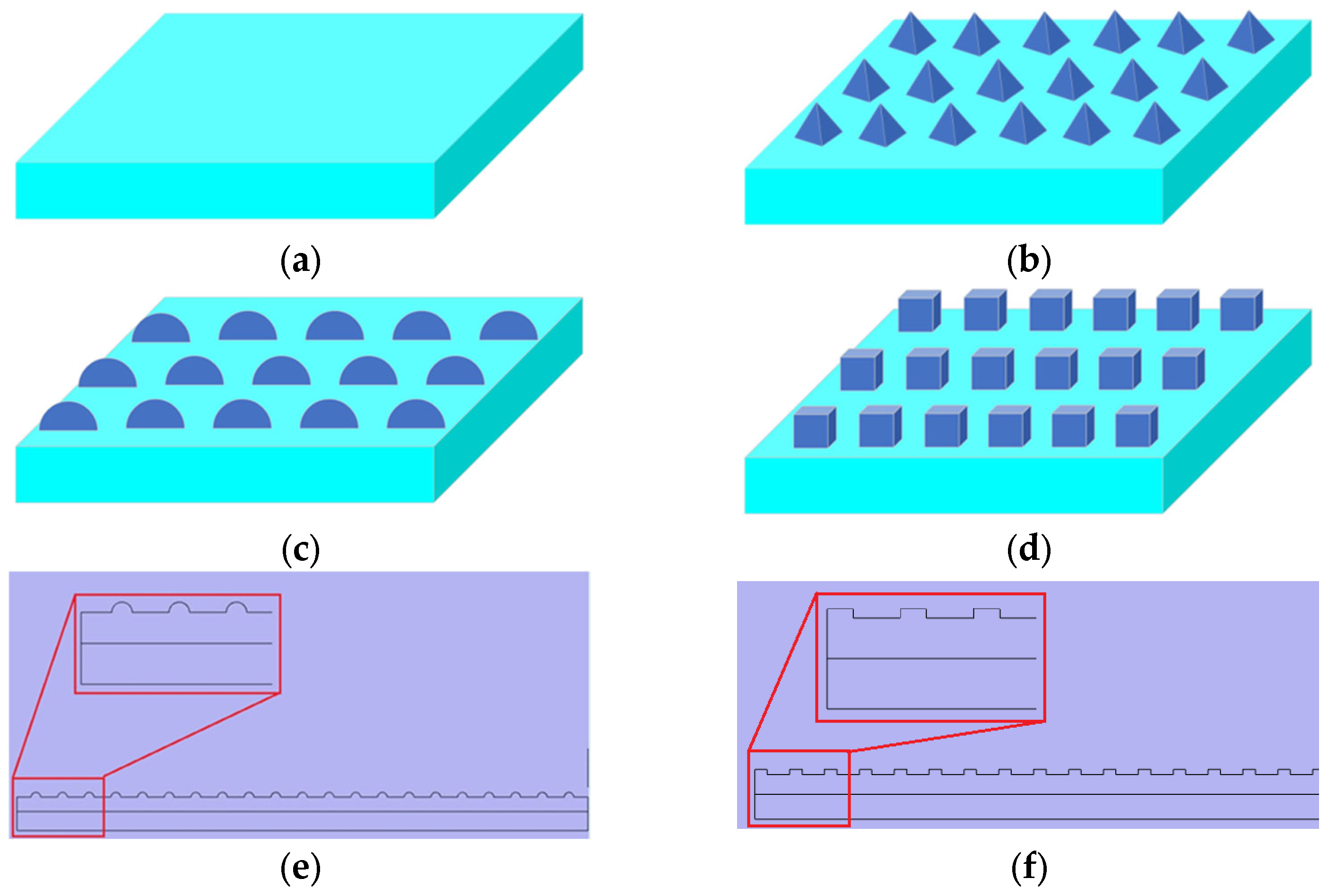
In this study, to achieve the best performance by micro-/nano-patterning, three designs of the structure are considered including pyramid, spherical, and cube. Then, the effect of patterned electrodes in four TENG modes is investigated under the same conditions. To reach this goal, the finite element method (FEM) is used for the simulation of the capacity of the designed TENG. In the first step, four modes of the TENG are simulated by consideration of flat surfaces and verified with references. In the next step, the effect of the shape of the pattern is investigated. So, the micro-patterned electrodes are designed and the electrical outputs are calculated. Finally, the electrical outputs are compared under the same condition to identify the effective pattern for each TENG mode. In the quest for improvement of TENG performance, this study’s approach, in selecting the most adaptive micro-patterns on dielectric surfaces based on TENG mode, heralds a transformative stride towards advancing the field, without added expenses related to fabrication.
2. Numerical Method and Working Principles
In this study, the finite element method by COMSOL Multiphysics is used to simulate TENG modes. The TENG principle is based on a parallel plate capacitor model [
23]. In the TENG layer, it is assumed that the electric field is perpendicular to these plates. The electric potential can be obtained by Maxwell’s and Gauss’s laws as Equations (1) and (2) [
23]:
where
D (C/m²) is the electric displacement field,
(C/m²) is space charge density,
V (V) is the output voltage, and
E (N/C) is the electrical field.
The electric field inside the dielectric layer is obtained by Equation (3). In Equation (3),
Q (C) is the induced charge,
S (m
2) is the surface area, and
εr (−) is the relative dielectric constant. In TENGs, dielectric layers and the air gap play a role in capacitance. After determining the equivalent capacitance of each layer, the governing equation of the output voltage for a contact-separation TENG mode is described by Equations (3) and (4) [
23]:
x (m) is the distance between the two triboelectric pairs,
(N/m
2) is surface charge density, and
d (m) is the layer’s thickness. The thickness, surface area, surface charge density, and relative dielectric constant are the inputs in the numerical model and then the output voltage is calculated based on Equation (4).
4. The Effect of Patterned Layer on TENG Performance
In this section, to provide the effect of pattern on the performance of the TENG, pyramid, spherical, and cube patterns are designed, and then the electric potential of the four TENG modes is investigated numerically. To select the dimension of the pattern, there are several studies in this area. Cheng et al. [
30] investigated PDMS surfaces treated with plasma at varying power levels and durations. In their study, the surfaces were treated with argon plasma before testing their output performance. By altering treatment parameters such as duration and plasma power, they achieved surfaces with different roughness levels and studied the relationships between these variables. During their work, a textured surface template was fabricated on a polished monocrystalline silicon wafer using the soft lithography method. This template featured pores with a diameter of 90 μm, a depth of 30 μm, and a spacing of 15 μm between each pore. According to their report, in a pillar array, the roughness after 15 min of treatment ranged from 150.06 nm to 140.40 nm. Kumar et al. [
31] investigated surface roughness and contact area using a novel Mica-PVS triboelectric nanogenerator. In their study, they created a wide range of surface roughness instances on the PVS surface (Sq from 1.5 to 82.5 µm) by replicating 3D-printed masters developed from numerically generated rough surfaces. Lee et al. [
32] studied interlocked interfaces to maximize output power by increasing the contact area, as demonstrated through simulations. In their study, the nano-pillar structures had uniform dimensions (diameter: 0.5 µm, pitch: 1 µm, height: 2 µm) and were arranged in a square array. Additionally, they examined a micro-cone Ni electrode with a bottom diameter of 2.5 µm, a height of 1.5 µm, and a pitch of 3 µm, arranged in a hexagonal array. Sriphan and Vittayakorn [
33] studied the fabrication of surface roughness and its effects on the electrical outputs of a triboelectric nanogenerator. In their study, solid salt was applied to create macroscopic triangle-like roughness on the material surface. Their study found that NaCl salt had an octahedron-like shape with an average particle size of around 200 μm. Wang et al. [
34] fabricated three types of regular and uniform polymer patterned arrays (line, cube, and pyramid) to enhance the efficiency of the nanogenerator. The size of individual PDMS features ranged from around 5 μm to 10 μm. Based on their work, the PDMS films with pyramid or cube structures demonstrated a nearly 5–6 times improvement in power generation compared to unstructured films. Choi et al. [
18] studied the impact of contact pressure on the output voltage of a triboelectric nanogenerator. They utilized PDMS pyramid arrays with different unit lengths: 2 μm (with 2 μm inter-pyramid spacing), 5 μm (with 5 μm inter-pyramid spacing), and 10 μm (with 10 μm inter-pyramid spacing). Despite the differences in unit length, the total surface areas of all three structures were the same. Their findings indicate that to effectively utilize the surface enlargement effect of interfacial micro- or nanostructures, sufficiently strong pressure must be applied to achieve a full-contact (FC) condition. Wang et al. [
35] investigated the effective contact area of micro-/nano-textured surfaces in triboelectric nanogenerators. The textures were designed as regular pyramid arrays. The study focused on examining the effects of texture pitch on both the contact area and the open-circuit voltage. The related parameters were set as follows: texture width a = 10 µm, texture height b = 7 µm, texture pitch c = 2 µm, 5 µm, and 10 µm, respectively. Based on various studies, the dimensions of nanostructures range widely from nanometers to micrometers. To create different morphologies, this study has decided to keep the number of roughness elements per unit area fixed. Consequently, the dimensions of the roughness shapes are calculated based on this constraint and selected to be in the micrometer range.
Figure 4 shows the 3D shape of the patterned layers. The roughness pattern detail is reported in
Table 2. Also, specific parameter settings for the simulation process are shown in
Table 3.
4.1. Pyramid-Patterned Layer Effects on In-Plane Sliding Mode
To investigate the effect of a patterned surface on TENG performance, a study is carried out on the TENG in in-plane sliding mode electrical output. The electric potential of the pyramid-patterned surface is shown in
Figure 5a. By increasing the dielectric distance from 0 mm to 30 mm, the voltage increases from 0 V to 233 V in the flat surface. After modification of the surface by the pyramid pattern, the voltage increases from 0 V at 0 mm to 321 V at 15 mm, and 328 V at 30 mm.
The results show that the voltage increases from 233 V in the smooth surface to 328 V in the pyramid-patterned surface. The significant increase in electric potential in the patterned surface as compared to the smooth surface proves the fact that energy output can be enhanced by the micro-patterned surface.
4.2. Pyramid-Patterned Layer Effects on Vertical Contact-Separation Mode
The electric potential for the TENG in contact-separation mode with the patterned surface is shown in
Figure 5b. The results show that the patterned surface has an impact on the overall output. In the flat layer, the voltage increases from 0 V at 0 mm to 195 V at 10 mm, and to 207 V at 15 mm. So, in the flat surface, the maximum voltage is around 207 V. By using the pyramid pattern, the voltage increases to 287 V, which is around 1.4 times higher than the flat surface.
4.3. Spherical- and Cube-Patterned Layer Effects on Vertical Contact-Separation Mode
Based on this study, the shape of the pattern is a key parameter that affects the performance of the TENG. To investigate the structure of the pattern, cube and spherical shapes of roughness are considered, as depicted in
Figure 2a,b. The results of the electrical outputs are shown in
Figure 6 and
Figure 7 for the cube and spherical shapes in the pattern, respectively. The electric potential distribution of the spherical pattern is shown in
Figure 6a–c for the contact-separation mode. By increasing the dielectric distance from 9 mm to 15 mm, the voltage increases from 304 V to 334 V. Also, the electric potential distribution of the cube pattern is shown in
Figure 6d–f for the contact-separation mode. By increasing the dielectric distance from 9 mm to 15 mm, the voltage increases from 269 V to 297 V in the cube pattern. Based on the results, in contact-separation mode, the spherical pattern produced a higher voltage than the cube-patterned layer. Based on this study, in contact-separation mode, it is better to keep the pattern shape close to spherical in order to improve efficiency.
4.4. Spherical- and Cube-Patterned Layer Effects on In-Plane Sliding Mode
Figure 7 shows the electric potential for spherical and cube patterns in sliding mode. In the spherical pattern, the voltage increases from 341 V at 15 mm to 348 V at 30 mm based on
Figure 7a,b. Also, in the cube pattern, the voltage increases from 377 V at 15 mm to 384 at 30 mm based on
Figure 7c,d. In the sliding mode, the cube pattern has a higher electrical output than the spherical pattern. The reason for the increasing voltage in the specific pattern is related to improving the surface area. Different shapes of the pattern produce a different effective surface area that is higher than the nominal surface area.
Table 4 presents a comparison of the electrical output among different modes and patterns.
According to previous studies in TENGs, enhancement of output performance can be achieved by material modification, increasing the contact area, and surface functionalization. In this study, based on surface modification, the effective contact area is bigger than the nominal surface area. So, by increasing the surface area, TENG layers accumulate more charges and then the charge transfer will increase. The actual surface charge density can be calculated based on the real contact area fraction (
) as Equation (5):
where
is the surface charge density under full contact.
Also, the real contact area will be increased by increasing external loads. On the other hand, in the TENG with a modified surface by patterns, contact with the moveable layer or slide on the fixed layer increases the TENG performance due to the friction and the heat production on the surfaces.
For the same surface pattern, such as a spherical pattern, the TENG output is compared in contact-separation mode and in-plane sliding mode. The results show that in contact-separation mode, the output is 344 V, whereas in in-plane sliding mode, it is 348 V. Additionally, for the pyramid pattern, the output in in-plane sliding mode is 328 V, while in contact-separation mode, it reaches 287 V. Based on the results, in sliding mode, the output is higher than in contact-separation mode for the same surface shape. This is due to the increased interaction between the layers during the contact mechanism. In sliding mode, the layers experience more friction, which leads to an increase in TENG output. Additionally, another factor contributing to the difference in TENG output is the type of contact. In contact-separation mode, the contact is point-to-point, whereas in sliding mode, due to the movement of the layers, the contact area between the surfaces increases.
The dynamics of each mode affect TENG performance and multiple factors need to be considered that may result in different outcomes in the two triboelectric modes. The differences in morphology between the two modes can be attributed to reasons such as type of contact, surface roughness, material used, applied force and pressure, time of the contact, and surface temperature. To facilitate comparison,
Table 5 presents the reasons for the effects of each mode and surface shape on TENG output.
Considering these factors, the difference in electrical output between the two TENG modes can be justified.
Also, it can be seen that the cube surface pattern has a higher electrical output compared to the spherical surface in in-plane sliding mode. Additionally, the spherical surface pattern has a higher output than other surface patterns in contact-separation mode. This can be explained by the physical and electrical properties of the surfaces and the interactions between them. For example, about the higher output in cube surface pattern at in-plane sliding mode it can be said that the cube surface has sharp edges and corners that create more contact with the opposing surface during sliding. This increase in contact points during sliding movement leads to higher electrical charge generation. Also, in sliding mode, the pressure is distributed more evenly across the cube surface. This even distribution can create more stable contacts, which contribute to generating higher electrical charges. In addition, the edges and corners of the cube in sliding mode create areas of high localized pressure, which can increase friction and, consequently, enhance the electrical output. But in the contact-separation state, due to the cubic surface having multiple edges and angles, forces are not evenly distributed across the surface. This non-uniform force distribution leads to a reduction in the generation of electric charges. Also, during separation, some contact points may not be properly separated due to the geometric shape of the cubic surface or may create weak point contacts, leading to lower electric charge production.
To illustrate the effect of surface pattern on electrical output, the contact-separation mode with a triangular surface pattern is shown in
Figure 8a–c. The maximum and minimum voltage values at vertical distances of 0 mm, 10 mm, and 15 mm are indicated in the color legend.
Figure 8d–f present a comparison of the effects of triangular and cubic patterns on the surface, in contrast to a flat surface.
4.5. Parametric Study on the Surface Roughness
In the next part, the effect of pattern dimensions is investigated. To study this, the height of the surface pattern is varied, and the impact of these changes is illustrated in
Figure 9. The roughness heights are considered with a variation of ±50%. The results show that by increasing the roughness height from 0.2 mm to 0.3 mm, the TENG output increases from 384 V to 458 V. Conversely, by decreasing the height by 50%, the output decreases from 384 V to 315 V. This reduction in height leads to a decrease in the effective surface area, causing the voltage to approach that of a flat surface.
The performance of TENGs is influenced by various factors such as the pressure between layers, tapping frequency, size, and compression of the patterns on the surfaces. This study does not include experimental tests, making it impossible to compare the results directly with other experimental data due to differences in design. However, several experimental studies have utilized the proposed surface patterns in their research and have demonstrated the repeatability of these results. Mohammadpour et al. [
36] demonstrated similar results to this study. They conducted computational modeling to investigate the excitation of neuronal cells using TENGs. They selected cube-, pyramid-, and sphere-shaped micro-patterns for the TENG layers. Their results showed that the output voltage for the cube-shaped TENG was higher than for the other two micro-patterns. This confirms that micro-patterns increase both the surface charge and the surface area. Lee et al. [
37] designed a square pyramid shape for a contact-separation TENG to achieve maximum power generation. They used aluminum and polytetrafluoroethylene (PTFE) as the TENG layers. Their experimental results showed an increase in output voltage of up to 67% with macroscale patterns that increased the surface area by 14%. In another experimental study, Zhang et al. [
38] placed a pyramid array shape on an aluminum film between two polydimethylsiloxane (PDMS) layers. The micro-/nano-dual-scale PDMS film with pyramid arrays demonstrated significantly enhanced performance, increasing the voltage by 100% and the current by 157% compared to a flat PDMS film.
To study the effect of roughness size on the correlation between surface patterns and TENG mode, the size of the surface pattern was adjusted to closely match the reference [
36]. The size of the roughness and the corresponding results are shown in
Table 6 and
Table 7, respectively.
Based on the new surface roughness size, decreasing the roughness size does not affect the results obtained from the previous section. The results confirm that the electrical output of the cube pattern is higher than that of the spherical pattern in in-plane sliding mode.
5. Conclusions
This study focused on identifying the best surface pattern that is adaptive to the TENG mode to improve performance. Although TENG performance improved with the patterned surface, the effectiveness of the patterns differed in different modes. In order to resolve this issue, four TENG modes were modeled by the FEM model on flat and patterned surfaces. To investigate the surface structure of the TENG performance, three surface patterns were designed such as pyramid, cube, and spherical. Then, the electrical outputs were studied under the same conditions. Based on this study, the performance of the TENG depends on the TENG mode and the pattern structure. According to the contact-separation mode, the sphere pattern produced a voltage of around 344 V, which is higher than the cube pattern, which produced a voltage of around 297 V. In sliding mode, the cube-patterned layer produced a voltage of around 384 V, which is higher than 248 V in the spherical pattern. As a result of this study, in sliding mode, the performance of patterned surfaces improves as they approach a cubic design. Furthermore, in a contact-separation model, it is better to design the pattern in a way that is close to a spherical pattern.


