Article

Correlation between the Dimensions and Piezoelectric Properties of ZnO Nanowires Grown by PLI-MOCVD with Different Flow Rates

1
Univ. Grenoble Alpes, Univ. Savoie Mont Blanc, CNRS, Grenoble INP, IMEP-LAHC, F-38000 Grenoble, France
2
Univ. Grenoble Alpes, CNRS, Grenoble INP, LMGP, F-38000 Grenoble, France
3
Univ. Grenoble Alpes, CNRS, CEA/LETI Minatec, Grenoble INP, LTM, F-38054 Grenoble, France
*
Authors to whom correspondence should be addressed.
Nanoenergy Adv. 2023, 3(3), 220-235; https://doi.org/10.3390/nanoenergyadv3030011
Submission received: 18 June 2023 / Revised: 26 July 2023 / Accepted: 28 July 2023 / Published: 2 August 2023

Abstract

:
Zinc oxide nanowires (ZnO NWs) have gained considerable attention in the field of piezoelectricity in the past two decades. However, the impact of growth-process conditions on their dimensions and polarity, as well as the piezoelectric properties, has not been fully explored, specifically when using pulsed-liquid injection metal–organic chemical vapor deposition (PLI-MOCVD). In this study, we investigate the influence of the O2 gas and DEZn solution flow rates on the formation process of ZnO NWs and their related piezoelectric properties. While the length and diameter of ZnO NWs were varied by adjusting the flow-rate conditions through different growth regimes limited either by the O2 gas or DEZn reactants, their polarity was consistently Zn-polar, as revealed by piezoresponse force microscopy. Moreover, the piezoelectric coefficient of ZnO NWs exhibits a strong correlation with their length and diameter. The highest mean piezoelectric coefficient of 3.7 pm/V was measured on the ZnO NW array with the length above 800 nm and the diameter below 65 nm. These results demonstrate the ability of the PLI-MOCVD system to modify the dimensions of ZnO NWs, as well as their piezoelectric properties.

Graphical Abstract

1. Introduction

ZnO is a multifunctional material with various interesting properties such as a wide direct bandgap energy (3.37 eV), a high exciton binding energy (60 meV), a high flexibility, a good visible transparency, and a high electron mobility, which makes it suitable for numerous applications [1,2,3,4]. In recent years, ZnO has attracted increasing attention as a promising alternative for lead-free piezoelectric devices because of its abundancy, biocompatibility, and attractive piezoelectric properties [5,6,7,8,9,10]. The first nanogenerator based on ZnO NWs were demonstrated by Z. L. Wang et al. in 2006 and 2007 [11,12]. Since then, various types of ZnO NW-based-nanogenerators have been developed using diverse fabrication techniques and designs [5,6,7,8,9,10]. For example, ZnO NWs can control the light emission intensity of light-emitting diodes (LEDs) and be integrated into a two-dimensional pressure distribution sensor, which has potential in many applications such as artificial skin, touch-pad technology, personalized signatures, bio-imaging, optical MEMS, and smart skins [13,14].
Among the various techniques to form ZnO nanostructures, metal–organic chemical vapor deposition (MOCVD) is capable of growing ZnO NWs with superior structural and optical quality at a high rate and on a large surface area without the need for an ultra-high-vacuum environment. All of the characteristics are suitable for industrial-scale production. Different research teams have investigated and demonstrated significant impacts of the growth temperature [15,16,17] and flow rates [18,19,20,21] on the ZnO formation during the MOCVD process, resulting in variations of its structural, optical, and electrical characteristics. For example, by using low-pressure MOCVD, L. Fanni et al. showed that different combinations of flow rates and temperatures can lead to different growth regimes, which significantly changed the ZnO growth directions and its properties [21]. Their results revealed that the ZnO-structured films have no preferential orientation at 250 °C, while it is mainly grown along the c-axis at 100 °C regardless of the flow rates. In contrast, our previous study on ZnO growth at higher temperatures ranging from 500 to 700 °C demonstrated a morphology transition from thin films to NWs [22]. Notably, at these elevated temperatures, both the thin films and NWs exhibit highly oriented structures along the c-axis. This preferential orientation can be attributed to the high temperature enhancing the diffusion of adatoms to the c-plane, where the reaction site is energetically favorable. Furthermore, D. Montenegro et al. also investigated the ZnO growth at 800 °C and demonstrated that the growth direction strongly depends on the flow rates. Different flow-rate conditions result in the formation of ZnO NWs with various lengths and diameters [20].
The variation of the dimensions of ZnO NWs can lead to a significant change of piezoelectric potential. This is because the free charge carriers, which can screen the piezoelectric potential within the NWs, are more effectively depleted in ZnO NWs with a smaller diameter [23,24]. Consequently, this reduces the screening effect and leads to an increase in the piezoelectric potential, as observed in the finite-element method (FEM) simulations shown by R. Tao et al. [23]. Additionally, A.J.L. Garcia et al. predicted a significant enhancement in the piezoelectric performance of ZnO NWs grown by MOCVD with the doping level of 1 × 1018 cm−3 when the radius is below 22 nm [24]. By using piezoresponse force microscopy (PFM) measurements, T. Jalabert et al. demonstrated that the piezoelectric coefficient of ZnO NWs grown by chemical bath deposition increases as the NW radius is decreased [25]. However, there is no systematic experimental investigation about the correlation between the diameters of ZnO NWs grown by MOCVD and their piezoelectric coefficient. Furthermore, the impact of the length of ZnO NWs on their piezoelectric properties has not been explored either.
In our previous study, we have grown ZnO thin films and NWs using the same pulsed-liquid-injection MOCVD (PLI-MOCVD) system while only adjusting the growth temperature from 500 °C to 700 °C [22]. In contrast to the traditional MOCVD system, the PLI-MOCVD utilizes the chemical precursor in its liquid state, eliminating the need for complex and cumbersome heating systems to maintain it in the vapor state. Additionally, the pulsed-liquid injection allows an accurate control of the precursor flow rate, enabling uniform and reproducible growth. Using the DataCube PFM measurements, we were able to directly compare the piezoelectric properties of those thin films and NWs fabricated by the same process, showing that NWs outperform thin films. We have also characterized the local piezoelectric properties and illustrated the alteration in polarity distribution between Zn and O polarity on thin films grown at 500 °C by varying the flow rate conditions, as shown in ref. [26]. In this study, we continue to study the impact of flow rates during the PLI-MOCVD process at 700 °C, for which the ZnO NWs are expected to be formed. The DEZn solution and O2 gas flow rates were sequentially varied. The field-emission scanning electron microscopy (FESEM) images show that all ZnO deposits are composed of NWs with different dimensions. The evolution of piezoelectric properties analyzed by the DataCube PFM technique as a function of the ZnO NW dimension is presented. The structural properties of ZnO NWs are also characterized using X-ray diffraction (XRD) and Raman spectroscopy.

2. Materials and Methods

2.1. ZnO NWs Grown by PLI-MOCVD

The ZnO NW samples were grown on heavily doped p-type Si (100) substrates by an Annealsys MC-200 PLI-MOCVD system. A solution of diethylzinc (DEZn, Sigma-Aldrich (Massachusetts, United States)) diluted in cyclohexane at 0.4 mol/L was used as Zn precursor during the PLI-MOCVD process. The O2 gas was used as O precursor. Two sample series were prepared: in the 1st series, the flow rate of O2 gas was varied in the range of 100 to 700 sccm, while the flow rate of DEZn solution was kept at 0.5 g/min. The flow rate of Ar gas was also adjusted to maintain the total gas volume introduced into the reactor chamber. In the 2nd series, the O2 flow rate was maintained at 500 sccm, while the DEZn flow rate was varied from 0.2 to 0.5 g/min. The growth temperature was set at 700 °C, and the chamber pressure was kept at 3 mbar for both sample series. The growth time was fixed at 8.45 min for all samples. The details of the precursor flow rates and their ratio used for ZnO depositions are shown in Table 1. The common sample for both series is the one grown with the 0.5 g/min DEZn solution and 500 sccm O2 gas flow rates (Sample 3 in Table 1).

2.2. Characterizations

2.2.1. Morphological and Structural Property Measurements

The morphology of ZnO NWs was observed by FESEM using a Quanta 250 FEI FEG-SEM. The XRD patterns were acquired with a Bruker D8 Advance diffractometer using CuKα1 radiation according to the Bragg–Brentano configuration. The Raman spectra were collected by using a Labram spectrometer (Jobin Yvon/Horiba, Longjumeau, France) equipped with a liquid-nitrogen-cooled charge-coupled device (CCD) detector. Since the ZnO NWs were grown on silicon substrates, cross-polarization was employed during the Raman scattering measurements to reduce the signals from the silicon substrates.

2.2.2. Piezoelectric Property Measurements

The piezoelectric properties of ZnO NWs were analyzed by using the DataCube PFM mode of a Bruker Dimension Icon AFM. A conductive tip (PtSi-NCH, Nanosensors (Neuchatel, Switzerland)) with a high spring constant of approximately 43 N/m was used to mitigate the interference of the electrostatic effect during the measurements [22]. In the DataCube PFM mode, the AFM tip was systematically brought into contact with the sample at a determined position, subsequently held in 60 milliseconds for the piezoelectric measurement, and then retracted before proceeding to the next position. This sequential approach and retraction of the AFM tip was employed to avoid tip dragging during the scanning process, which could bend the NWs and cause a contact failure between the AFM tip and the sample. When the AFM tip was in contact with the sample, an AC voltage of 5 V amplitude and 15 kHz frequency of AC voltage was applied across the top and bottom of the sample through the tip and chuck of the AFM system. Due to the piezoelectric properties, the ZnO NWs were deformed in response to the AC voltage. This deformation was measured by the AFM tip to obtain the piezoelectric response amplitude and phase signals. The piezoelectric response amplitude is proportional to the piezoelectric coefficient, while the piezoelectric response phase identifies the polarity of ZnO NWs [22]. Thanks to the small radius of the AFM tip (i.e., ~25 nm), the piezoelectric response of each individual NW can be measured. By scanning the AFM tip across a 1 × 1 µm2 area, the piezoelectric response of the NWs in the array was mapped. For each sample, the piezoresponse amplitude values were extracted from the piezoresponse amplitude map, and the mean piezoresponse amplitude was evaluated to study the piezoelectric amplitude behavior of ZnO NWs grown at different flow rates. The mean piezoresponse amplitude was calculated using the following formula:
M e a n   p i e z o r e s p o n s e   a m p l i t u d e = P i e z o r e s p o n s e   a m p l i t u d e   o f   p i x e l   i   N u m b e r   o f   c o n s i d e r e d   p i x e l

3. Results

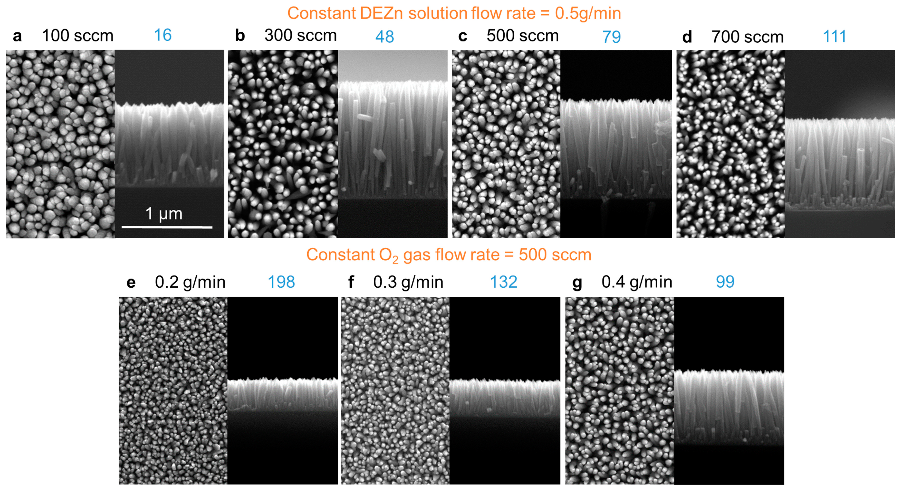
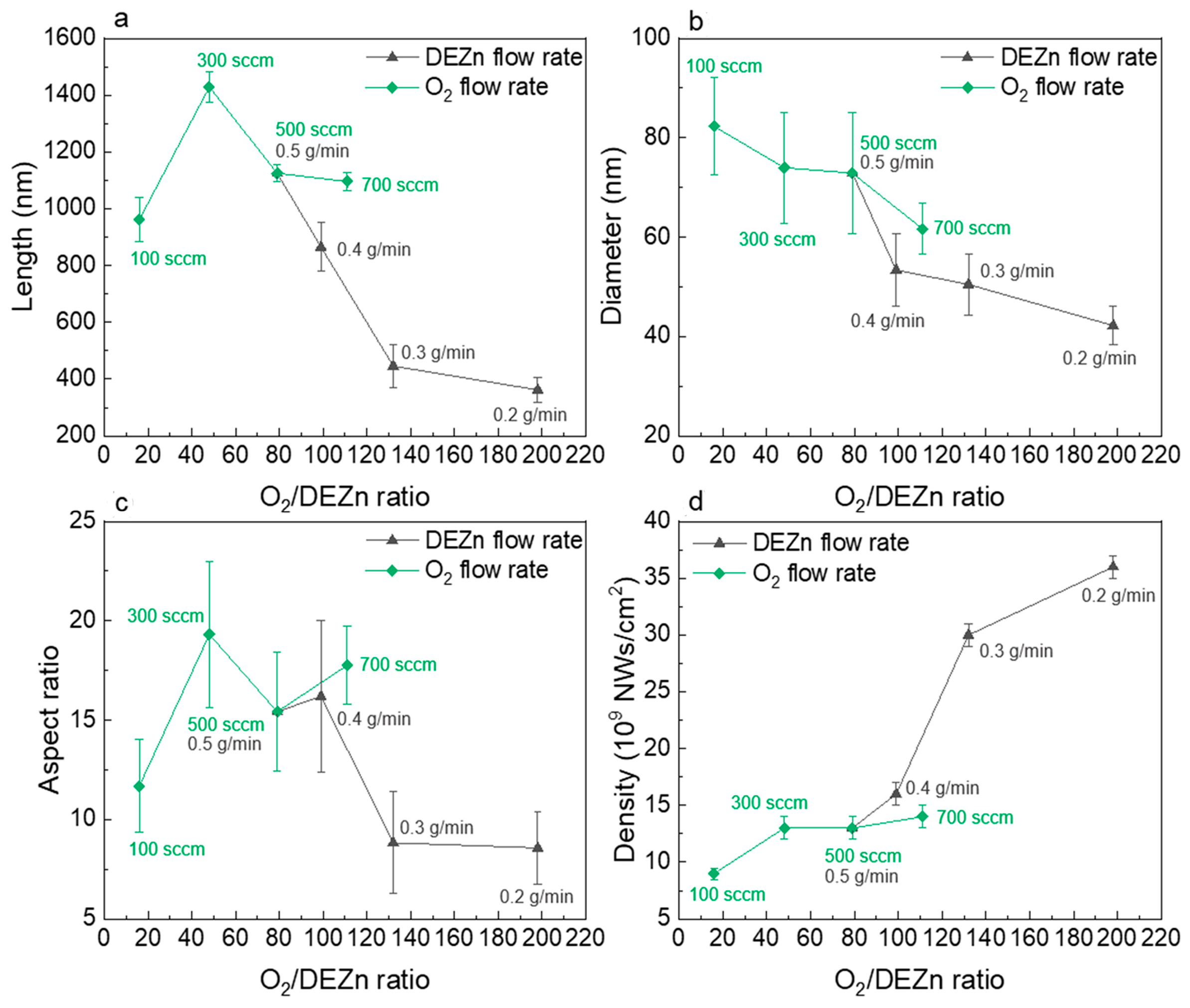
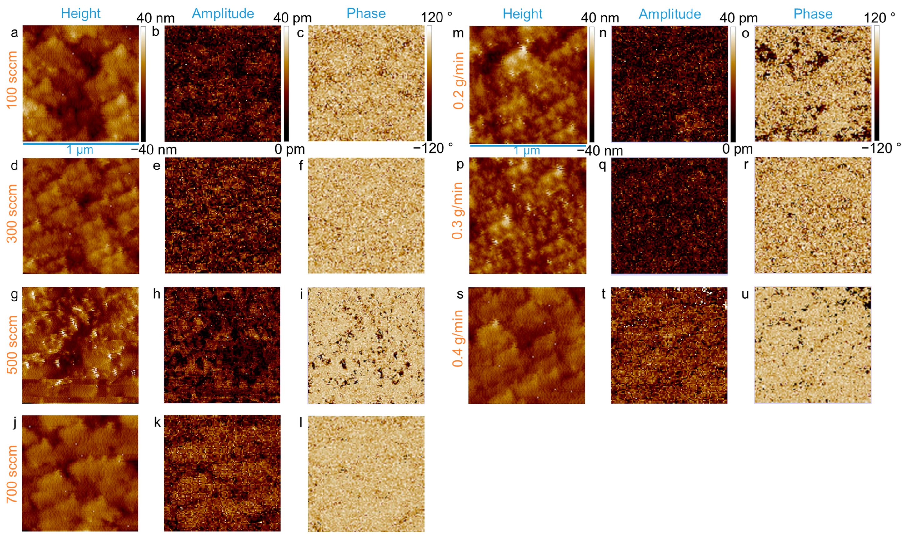
3.1. Morphological Properties

Figure 1 displays the FESEM images of ZnO deposits grown on Si substrate at 700 °C using the PLI-MOCVD system, showing that all the growths result in the formation of vertically aligned NW arrays regardless of flow-rate conditions. In comparison to our previous study shown in ref. [26], in which the same system and growth conditions were used, except for the growth temperature being set at 500 °C, all the growths at that lower temperature led to the formation of ZnO thin films. This observation indicates that the temperature plays a dominant role in the ZnO growth by PLI-MOCVD, leading to the formation of either thin films or NWs. The transition of ZnO morphology from stacked thin film to NWs when the growth temperature increases from 500 to 700 °C was also demonstrated in our earlier research shown in ref. [22]. The reason is due to the fact that Zn and O adatoms tend to diffuse and develop on the polar c-planes with the highest surface energy [1], and hence, the formation process of ZnO is driven by the minimization of the free energy. The strongly anisotropic growth along the polar c-axis combined with the significant desorption of Zn and O atoms from the substrate at the high growth temperature of 700 °C leads to the formation of isolated islands with a high c-axis orientation at the beginning of the growth. Then, the subsequent elongation of NWs on those islands because of the enhanced surface diffusion of Zn and O adatoms at high temperature results in the formation of vertically aligned NW arrays. In another MOCVD system, D.N. Montenegro et al. demonstrated that the ZnO morphology transformed from NWs to a thin film when the nitrous oxide (N2O) flow rate was increased, while the flow rate of dimethylzinc–triethylamine (DMZn–TEN) was maintained, corresponding to the increase in the O/Zn precursor flow-rate ratio [20]. Their results showed that the higher O/Zn flow-rate ratio leads to a less anisotropic growth explained by the reduction in the surface diffusion of Zn adatoms toward the growing surfaces (i.e., the c-planes on the NW tips), resulting in the formation of thin films. They also showed that the lengths and diameters of ZnO NWs were changed with the variation of N2O and DMZn–TEN flow rates. In our case, Figure 1 also shows the variation of NW length and diameter when the O2 gas and DEZn solution flow rates are changed, expressing the impact of the flow-rate conditions on the formation process of ZnO NWs, as well as their axial and radial growth rates [27,28,29]. The length, diameter, aspect ratio (length/diameter ratio), and density of ZnO NWs were extracted from FESEM images and presented in Table 2. Their evolutions as a function of the O2/DEZn molar flow-rate ratio are shown in Figure 2.
The NW length is driven by the growth rate in the axial direction, and the NW diameter is driven by the growth rate in the radial direction. When the DEZn solution flow rate is increased from 0.2 to 0.5 g/min while the O2 gas flow rate is kept constant at 500 sccm, both the length and diameter of the ZnO NWs continuously increase (Figure 2a,b). This implies that the growth of ZnO NWs is limited by the DEZn reactant in this range of flow-rate conditions. In Figure 2c, the aspect ratio of ZnO NWs also increases as the DEZn solution flow rate is increased from 0.2 to 0.4 g/min, expressing the faster increase in the growth rate in the axial direction compared to in the radial direction. In contrast, the aspect ratio of ZnO NWs decreases as the DEZn solution flow rate is further increased to 0.5 g/min, showing that the growth starts to be less anisotropic.
In the other sample series, when the DEZn solution flow rate is kept at 0.5 g/min, both the length and diameter of ZnO NWs increase when the O2 gas flow rate is decreased from 700 to 300 sccm. However, when the O2 gas flow rate is further decreased to 100 sccm, the length drastically decreases while the diameter continues increasing (Figure 2a,b). The decrease in NW length observed at a 100 sccm O2 gas flow rate indicates that the O2 reactant starts to be insufficient, hampering the growth of NW in the axial direction. Meanwhile, the increase in the diameter at this 100 sccm O2 flow rate could also be attributed to a deficiency in O2 reactant reaching the most reactive site at the top of the NWs. Thus, the DEZn reactants start attaching to other nonpolar planes (such as the m-planes) at the sidewall of the NWs where the surface energy is lower, leading to the development of ZnO in the radial direction.
Figure 2a,b also show that both the NW length and diameter tend to increase as the O2/DEZn molar flow-rate ratio is decreased from 198 down to 48, expressing that the growth regime is limited by the DEZn reactants. When the O2/DEZn flow-rate ratio is further decreased to 16, the NW length starts decreasing, indicating a transition to a growth regime limited by the O2 gas reactant. In addition, Figure 2d illustrates that the density of ZnO NWs also tends to decrease as the O2/DEZn flow-rate ratio is decreased. This can be explained by the correlation between the density and the diameter of ZnO NWs. For instance, at the lowest O2/DEZn flow-rate ratio (i.e., 16), the NW array has the largest diameter, which is a result of the merging of many smaller NWs during the growth process. As a consequence, the number of NWs decreases, leading to its lowest density. In contrast, the sample grown at the highest lowest O2/DEZn flow-rate ratio (i.e., 198) has the smallest NWs before merging, and hence, its density value is the highest one.

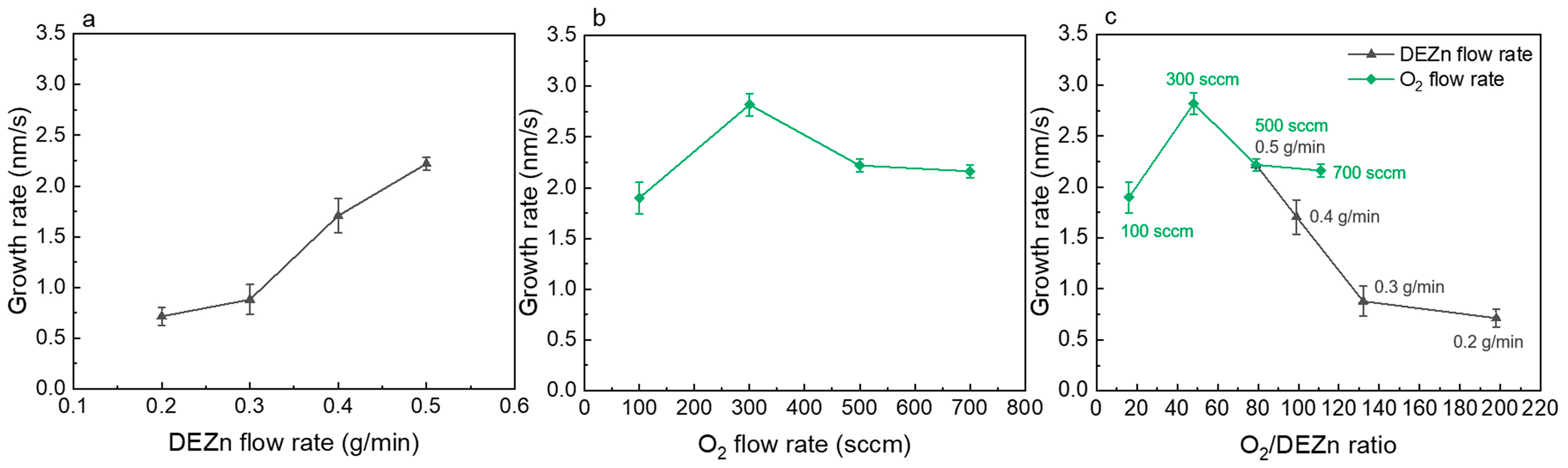
3.2. Growth Rate of ZnO NWs

The growth rate of ZnO NWs depending on the flow-rate conditions was approximately estimated by calculating the ratio of their length over the growth time, as presented in Figure 3. While the O2 gas flow rate is kept constant at 500 sccm, Figure 3a shows that the growth rate of ZnO NWs rapidly increases from 0.7 to 2.2 nm/s when the DEZn solution flow rate is increased from 0.2 to 0.5 g/min. The increase in the growth rate with the DEZn solution flow rate indicates that the growth of ZnO NWs at 700 °C is limited by the amount of DEZn reactant in the PLI-MOCVD chamber. On the other hand, while the DEZn solution flow rate is maintained at 0.5 g/min, the growth rate of ZnO NWs increases from 1.9 to 2.8 nm/s when the O2 gas flow rate is increased from 100 to 300 sccm (Figure 3b). The slower growth rate at a 100 sccm O2 flow rate shows that O reactants are insufficient at a low O2 gas flow rate. In contrast, the growth rate also decreases and maintains at 2.2 nm/s when the O2 gas flow rate is further increased to 500 and 700 sccm. It is worth mentioning that the pressure was maintained at 3 mbar, and the total gas volume introduced into the PLI-MOCVD chamber was kept constant by adjusting the flow rate of Ar gas to compensate for the amount of O2 gas that was varied. Thus, the decrease in the growth rate of ZnO NWs at a higher O2 gas flow rate could be due to the increase in the reaction between the O and Zn reactants in their gas phase, which interfered with the Zn reactants diffusing to the substrate to form ZnO NWs. Nevertheless, Figure 3c shows that the NW growth at 700 °C is limited by O reactants when the O2/DEZn flow-rate ratio is below 48, while it is limited by Zn reactants when the O2/DEZn ratio is higher.
Additionally, determining the growth rate of an NW array solely based on its length over the growth time can result in an inaccurate estimation, since there are also the differences in NW diameter and density, as well as in the area coverage among NW arrays. To obtain a more accurate equivalent growth rate, we also calculate the ratio of the total ZnO volume per cm2 over the growth time, as shown in Figure S1. The evolution of the growth rate deduced from the volume/growth time with the flow-rate conditions in Figure S1 is consistent with the growth rate calculated from the length/growth time in Figure 3c, thereby confirming the NW growth-rate tendency with the DEZn and O2 flow-rate variation, as shown above.

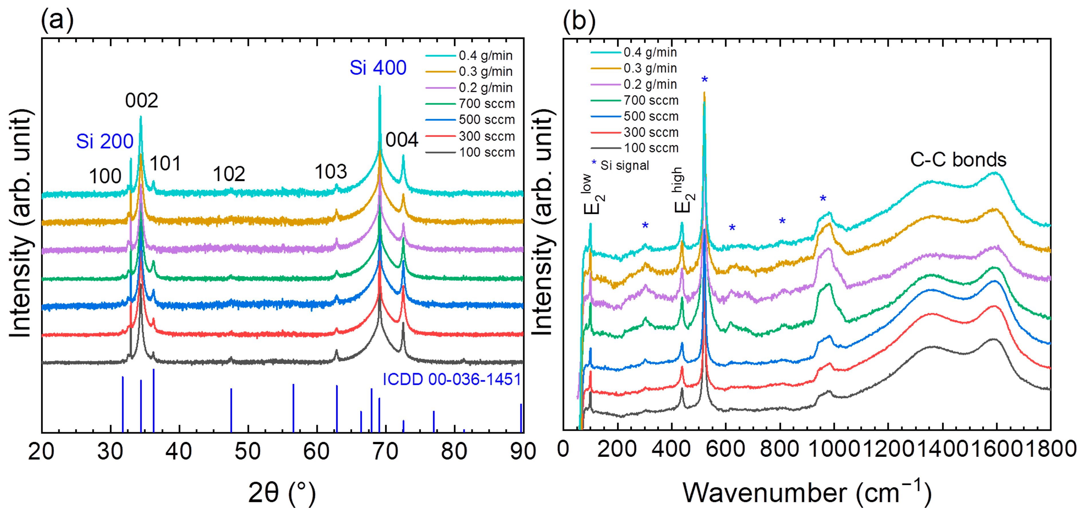
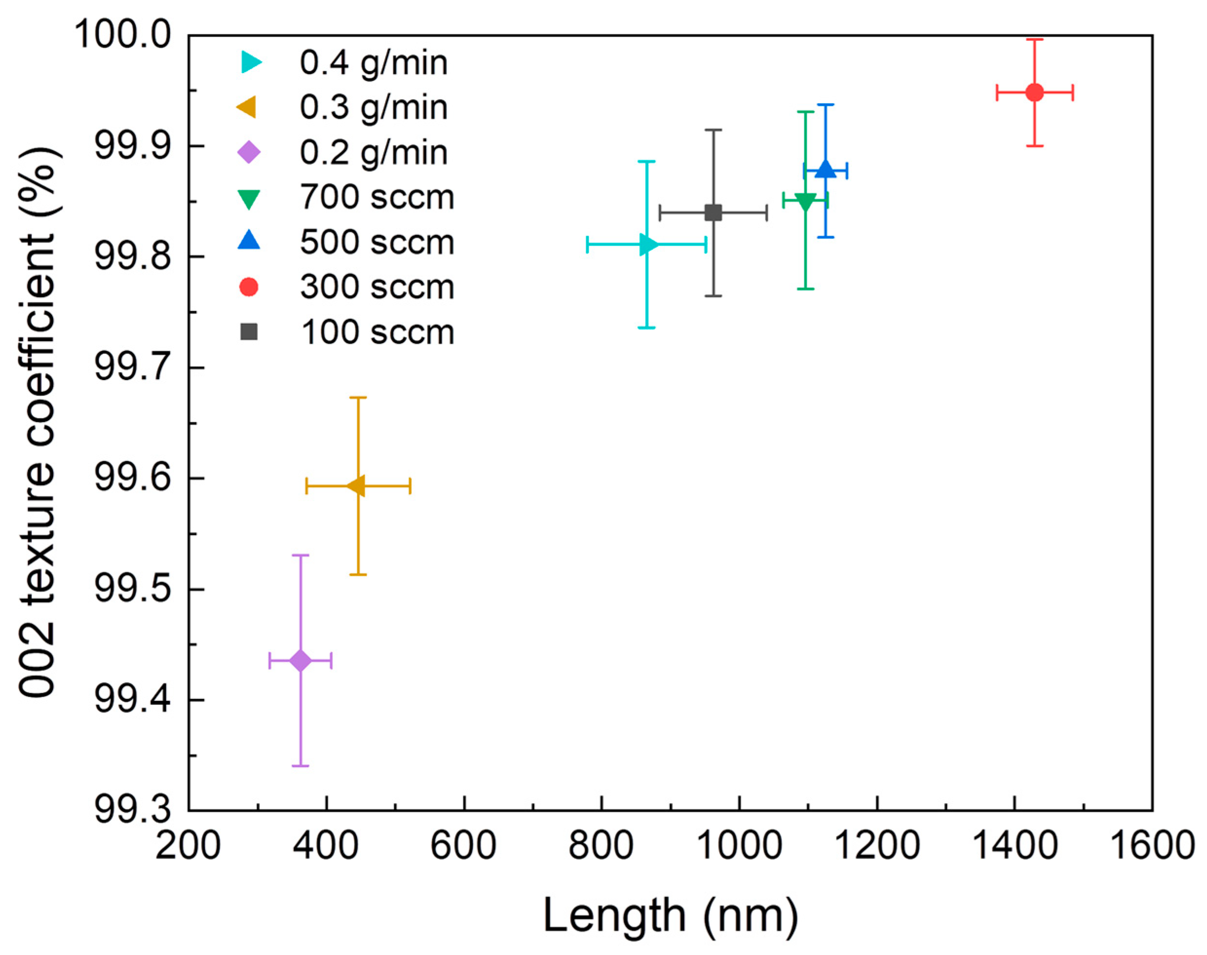
3.3. Structural Properties of ZnO NW Arrays

The structural properties of NW arrays were analyzed by XRD and Raman spectroscopy. The XRD patterns of ZnO NWs in Figure 4a show the 100, 002, 101, 102, 103, and 004 diffraction peaks of the ZnO wurtzite structure located at 31.8, 34.4, 36.3, 47.5, 62.9, and 72.6°, respectively, according to the ICDD file labeled 00-036-1451. Correlatively, their Raman spectra in Figure 4b also show the E2low and E2high lines of the ZnO wurtzite structure positioned at 99 and 438 cm−1, respectively [30,31]. The signals detected at around 1360 and 1580 cm−1 in their Raman spectra are assigned to the C-C bonds. This indicates that organic compounds as by-products from the general chemical reaction during the PLI-MOCVD process are formed and, hence, that carbon impurities may be incorporated into ZnO NWs [32], which is similar to our investigation dedicated to ZnO thin films grown by the same system, as shown in ref. [26]. Interestingly, the XRD patterns of ZnO NW arrays, however, display a significantly sharper 002 diffraction peak than those of ZnO thin films. The E2low and E2high lines of ZnO NWs are also more intense as compared to those of ZnO thin films in the Raman spectra. This reveals the superior crystallinity of ZnO NWs grown at 700 °C as compared to the ZnO thin films grown at 500 °C using the same PLI-MOCVD system and flow-rate conditions.
The intensity and position of diffraction peaks in the XRD patterns of ZnO NW arrays were exploited to evaluate the structural orientation and residual homogeneous strain. The structural orientation was assessed by the texture coefficients Chkl (in percentage units) of (hkl) planes, which were calculated using the following equation [33]:
C h k l % = I h k l I 0 ,   h k l × 100 Ʃ i = 1 N I h i k i l i I 0 ,   h i k i l i
where Ihkl is the hkl peak intensity, I0,hkl is the reference hkl peak intensity from the 00-036-1451 ICDD file, and N (i.e., 5) is the number of diffraction peaks considered. The residual homogeneous strain is an estimate of the mean residual strain inside the ZnO structure at the end of the PLI-MOCVD process and was calculated as follows:
ε h s = c c o c o × 100
where co = 5.2066 Å is the theoretical c-lattice parameter of the wurtzite structure of ZnO extracted from the 00-036-1451 ICDD file. The actual c-lattice parameter value was deduced from the 002 diffraction-peak position by using Bragg’s law equation:
λ = 2 d sin θ
where λ is the wavelength of the Cu Kα1 source equal to 0.15406 nm, θ is the Bragg angle of the 002 diffraction peak, and d is the spacing between two consecutive (002) planes and equal to half the c-lattice parameter in the wurtzite structure.
Overall, the 002 texture coefficients of ZnO NW arrays are above 99.4%, expressing their very high orientation along the polar c-axis (see Figure S2a). The increase in the 002 texture coefficient of ZnO NWs with their length is observed in Figure 5 and is due to the fact that the signal of the 002 diffraction peak is larger when coming from the longer ZnO NWs. This again implies that ZnO NWs get more oriented along the polar c-axis during their elongation. Also, the contribution coming from the ZnO nucleation layer beneath ZnO NWs is less when they are longer. The residual homogeneous strains of ZnO NW arrays lie in the range of 0.02 to 0.07% and, thus, are low, implying the efficient strain relaxation because of their geometry (see Figure S2b). In comparison, the residual homogeneous strains of ZnO thin films grown by PLI-MOCVD using the same system as reported in ref. [26] are varied from −0.01 to −0.4%. In agreement with the XRD analysis, the position of the E2high line in the Raman spectra of ZnO NW arrays is very close to the bulk value pointing at 438 cm−1, indicating again that they are fully relaxed.

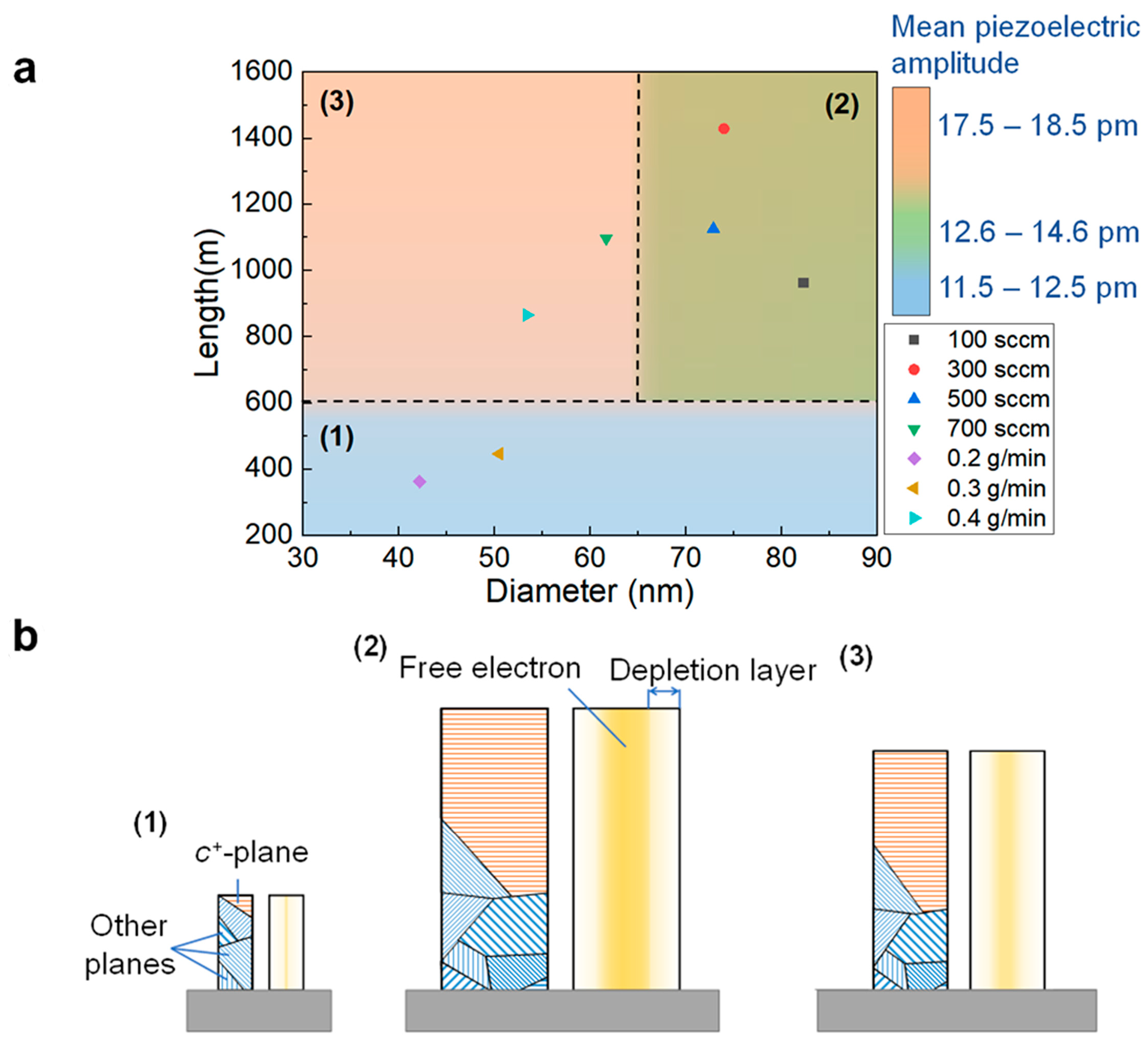
3.4. Crystal Polarity and Piezoelectric Response

3.4.1. Crystal Polarity

Figure 6 illustrates the PFM maps of the NW array, presenting the piezoelectric responses of every NW within the 1 × 1 µm² area. The piezoelectric response amplitude is proportional to the piezoelectric coefficient and applied voltage amplitude, while the piezoelectric response phase with respect to the applied voltage indicates the polarity. The positive phase value at around 70° (bright area) corresponds to the Zn polarity, and the negative phase value at around −90° (dark area) corresponds to the O polarity [22]. The amplitude images of NW arrays grown with different flow-rate conditions exhibit different brightnesses, expressing a variation of the amplitude, as well as the piezoelectric coefficient, among NW samples.
In their phase images, the predominance of the positive phase (bright area) indicates that ZnO NWs have Zn polarity. Some small dark areas in those phase images do not represent the O-polar ZnO NWs, but they are artifacts resulting from the contact failure when the AFM approached the void between NWs. This is due to the fact that we did not fill the void in the NW arrays before performing the PFM measurement. In our earlier work shown in ref. [22], the void in the NW array was filled by poly(methyl methacrylate) resist (PMMA), on top of which the PFM measurement gave nonpolar responses, since the PMMA is a nonpiezoelectric material. The PFM results of ZnO NW arrays show that all NWs grown by the PLI-MOCVD process at 700 °C are Zn polar, regardless of the flow-rate conditions. This is different from the thin films grown by the same process but at 500 °C, where there are predominant Zn-polar, predominant O-polar, and coexisted two-polar thin films formed at different O2/DEZn flow-rate ratios, as shown in ref. [26]. To verify if the O-polar ZnO NWs can be grown by our PLI-MOCVD process, we performed another NW growth on ZnO substrates (from Crystec) with identified Zn and O polarities. The DEZn solution and O2 gas flow rates were set to 0.5 g/min and 500 sccm, respectively. Other parameters were kept the same as those of the NW growths on Si substrates shown in this study. The piezoelectric-phase-response images obtained from PFM again show that all ZnO NWs have Zn polarity regardless of the polarity of the ZnO substrates (Figure S3), confirming that only Zn-polar ZnO NWs were grown by the PLI-MOCVD process.
This finding is consistent with the results of G. Perillat-Merceroz et al. shown in ref. [34], in which the ZnO NWs were grown on O-polar ZnO substrate by MOCVD using DEZn as the Zn precursor and N2O as the O precursor. Their convergent beam electron diffraction measurement also demonstrated that ZnO NWs are Zn polar and sit on top of O-polar pyramids. In the work of V. Sallet et al., they also showed that the catalyst-free ZnO NW growth by MOCVD resulted in Zn-polar ZnO NWs, while the O-polar ZnO NWs were only formed using the catalyst-assisted approach with a gold droplet [35]. Similarly, Z.L. Wang et al. showed that the Zn clusters, as well as the local Zn enrichment at the growth front, only occurred on the Zn-terminated ZnO (001) polar surface, leading to the self-catalyzed growth of the ZnO NW during the vapor–liquid–solid (VLS) growth process, while the O-terminated (00 1 - ) polar surface was chemically inert and did not initiate any growth [36]. In another study, P. X. Gao and Z. L. Wang demonstrated that both O- and Zn-polar ZnO surfaces were chemically active by adding the tin (Sn) element as a catalyst for VLS growth [37]. Different from the catalyst-free growth of the MOCVD process, the ZnO NWs grown by chemical bath deposition can be controlled to be along either the Zn- or O-polarity direction. This is achieved by performing the ZnO growth on the ZnO substrate with either the Zn or O polarity, respectively [38]. Although the ZnO NWs grown by our PLI-MOCVD are limited to the Zn polarity, the uniformity of the polarity of the NW array is essential for highly efficient piezoelectric devices.

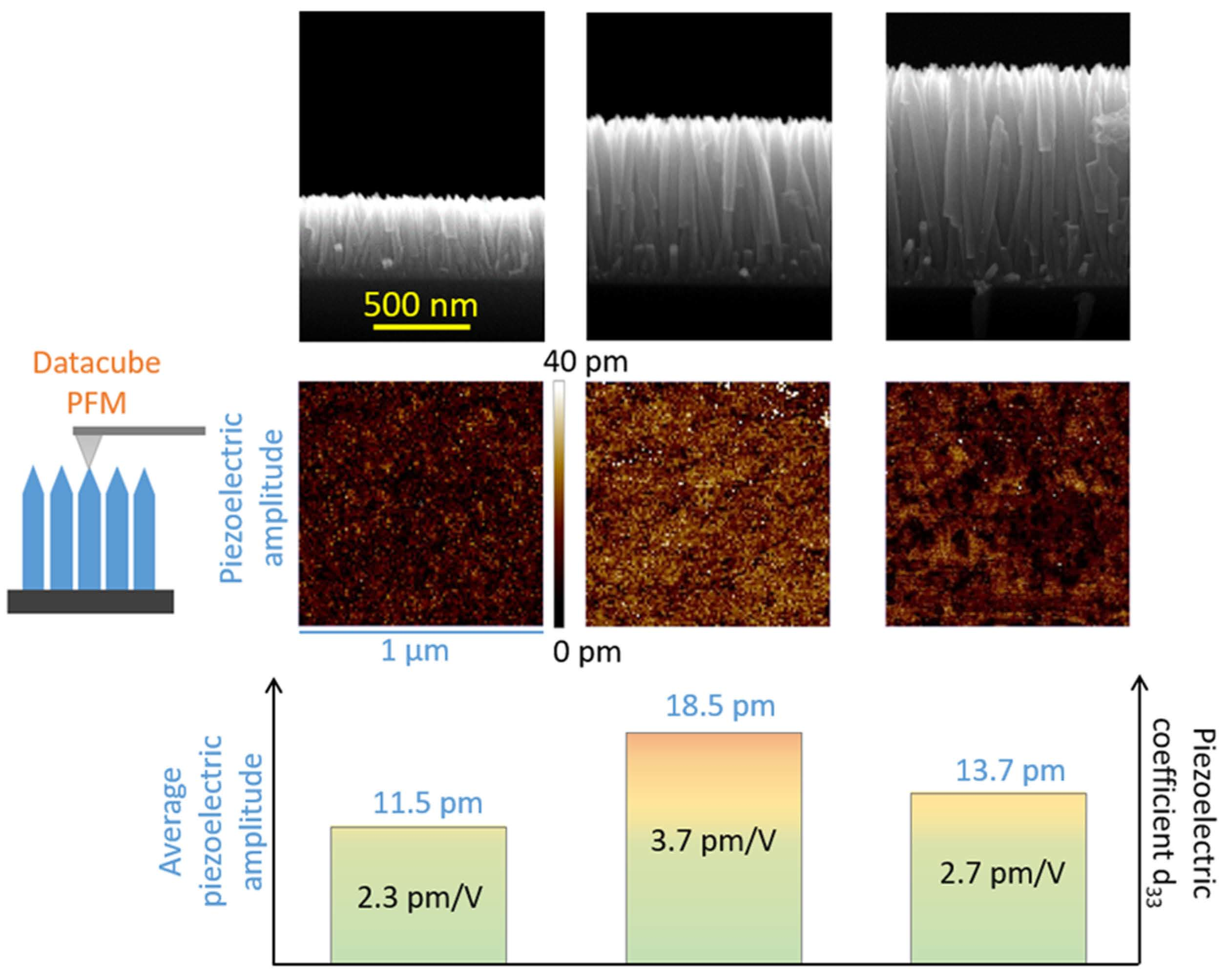
3.4.2. Piezoelectric Amplitude and Coefficient

In order to study the influence of flow-rate conditions on the piezoelectric amplitude of ZnO NWs, the mean piezoelectric amplitude on the Zn-polar NWs was extracted from their piezoelectric amplitude images. The mean amplitude calculation only took into account data points with a piezoelectric phase higher than 50° assigned to the Zn-polar signals from NWs. Other data points were assigned to artifacts from the void in the NW array and were removed.
Figure 7 presents the evolution of the mean piezoelectric amplitude of ZnO NWs as a function of the length, diameter, aspect ratio, and density of the NW arrays, corresponding to their flow-rate growth conditions. In Figure 7a, the graph shows that the amplitude seems to be higher on the longer NWs, except on two NW arrays grown with the 0.4 g/min DEZn solution and 700 sccm O2 gas flow rates, which exhibited the highest performance despite having a medium length. On the other hand, there is a clearer tendency of decrease in amplitude when the NW diameter is increased, as presented in Figure 7b. However, two NW arrays grown with the 0.2 and 0.3 g/min DEZn solution flow rate exhibit the lowest amplitude despite their smaller diameters, which could be due to their shortest length as observed in Figure 7a. Similarly, the amplitude also exhibits a strong dependence on the NW aspect ratio in Figure 7c, in which it increases when the aspect ratio increases. The NW array grown with the 300 sccm O2 gas flow rate has the highest aspect ratio, but it has the lower amplitude compared to two NW arrays grown with the 0.4 g/min DEZn solution and 700 sccm O2 gas flow rates, for which the NW diameters are smaller (Figure 7b). In Figure 7d, except for the two NW arrays grown with the 0.2 and 0.3 g/min DEZn solution flow rate, the piezoelectric amplitude likely increases as the NW density is increased. The change of the piezoelectric amplitude with the NW density can be explained by the influence of the growth process: as the NWs grow, smaller NWs tend to merge and coalesce to form larger NWs. Consequently, the NW diameter increases as the NW density decreases. Since the area coverage among NW arrays is similar, the density of ZnO NWs is approximately inversely proportional to the diameter square (see Figure S1a and Equation (S2) in supplementary information). Thus, the evolution of the piezoelectric amplitude with the NW density observed in Figure 7d is due to its correlation with the diameter.

4. Discussion

The variation of the piezoelectric amplitude, as well as its correlation with the dimension of ZnO NW arrays grown by PLI-MOCVD for different flow-rate conditions, can be attributed to several physical phenomena.
First, it is shown by XRD that the orientation of ZnO NWs along the polar c-axis is improved when their lengths are increased (Figure 5), which is favorable for enhancing the piezoelectric amplitude. This could be a reason for the lowest piezoelectric amplitude in the shortest ZnO NWs grown with the 0.2 and 0.3 g/min DEZn solution flow rate. These findings are consistent with the FEM simulations reported in ref. [24], in which the increase in the length of ZnO NWs is expected to lead to the improvement of their piezoelectric performance.
Second, ZnO NWs with a small diameter or a high aspect ratio can provide a large sidewall surface area, on which the surface Fermi level pinning occurs in turn, depleting the free charge carriers in their bulk [23,24]. The free charge carriers are depleted more effectively in ZnO NWs with a smaller diameter, leading to reducing the screening effect and increasing the piezoelectric potential [23,24]. Thus, the piezoelectric amplitude of ZnO NWs tends to increase as their diameter is decreased or their aspect ratio is increased, as shown in Figure 7b,c. The degree of influence of those physical phenomena on the piezoelectric amplitude also depends on the length and diameter of ZnO NWs, which can be illustrated by three regimes, as shown in Figure 8. In regime (1), the ZnO NWs grown with the 0.2 and 0.3 g/min DEZn solution flow rate have very short lengths (362 and 446 nm, respectively), on which the piezoelectric amplitude is the lowest despite their smallest diameter. This implies that the piezoelectric amplitude is more limited by the short lengths of ZnO NWs rather than by their diameters. The reason for this can be explained as follows: during the early stage of the growth of ZnO NWs, a polycrystalline thin-film structure is formed (Figure 8b). This leads to the presence of diverse domains with different piezoelectric polar directions in short-length NWs, which is not favorable for the piezoelectric response in these structures. As the NWs grow longer, a large-sized monocrystal containing ZnO NWs with orientations along the polar c-axis is eventually formed, resulting in enhancing the piezoelectric response when the NW length reaches a sufficient value.
However, in regime (2), the ZnO NWs grown with the 300 sccm O2 gas flow rate have the longest length and the highest aspect ratio, but they exhibit a larger diameter and, hence, a lower piezoelectric amplitude as compared to the ZnO NW arrays grown with the 700 sccm O2 gas flow rate and the other one grown with the 0.4 g/min DEZn solution flow rate. This indicates that the NW diameter now plays a significant role in the piezoelectric response.
The highest piezoelectric amplitude is observed in ZnO NWs grown with the 0.4 g/min DEZn solution flow rate, which has the third-smallest diameter but has a length above 800 nm. This NW array is situated in regime (3), where the ZnO NWs have a better c-axis-oriented structure because of its longer length and fewer residual free electrons because of the more efficient depletion phenomenon on the thinner NW. These results express that the piezoelectric amplitude is stronger for the NWs with lengths above 800 nm and diameters smaller than 65 nm. The experimental diameter is larger than the predicted 44 nm diameter for ZnO NWs grown by MOCVD with a doping level at 1 × 1018 cm−3 and surface trap density at 1 × 10¹² eV−1 cm−2, as shown in the report of A.J.L. Garcia et al. [24]. This could be due to the difference in the doping concentration or the surface trap density, which also have a significant impact on the piezoelectric properties of ZnO NWs.
Third, the variation of the flow-rate conditions can influence the incorporation of defects and impurities into ZnO NWs during their growth [39], which in turn affects the screening effect, as well as the piezoelectric response [23]. Investigations into the doping concentration and surface trap density on ZnO NWs could be conducted to further understand their effects on the piezoelectric properties. Nevertheless, the findings from this study show that the evolution of the piezoelectric amplitude is, overall, governed by the dimensions of ZnO NWs, while the variations of the doping concentration and surface trap density may have a minor effect. In addition, the mean piezoelectric amplitude of ZnO NWs is varied from 11 to 19 pm. In comparison, the ZnO thin films grown with the same PLI-MOCVD system but at a lower growth temperature have their mean piezoelectric amplitudes on the Zn-polar domain in the range of 8 to 11 pm, as shown in ref. [26]. Since the applied voltage amplitude in PFM measurements was kept at 5 V, the deduced piezoelectric coefficient d33 lies in the range of 2.2 to 3.7 pm/V for ZnO NWs and 1.6 to 2.2 pm/V for ZnO thin films. This emphasizes that the ZnO NWs have superior piezoelectric efficiency compared to ZnO thin films.

5. Conclusions

In summary, we have demonstrated the growth of ZnO NWs by PLI-MOCVD with different combination of O2 gas and DEZn solution flow rates. Our results show that ZnO NWs were formed under all flow-rate conditions. The lengths and diameters of ZnO NWs were varied by adjusting the flow-rate conditions, indicating their impacts on the axial and radial growth rates and revealing different growth regimes limited either by the O2 gas or DEZn reactants. The XRD and PFM analyses have revealed that the ZnO NWs were grown along the c+- direction (Zn polarity) of the wurtzite structure, which is in agreement with other research on the spontaneous growth of ZnO NWs using MOCVD. While the ZnO NW grown by our PLI-MOCVD process was limited to Zn polarity, the formation of a ZnO NW array with uniform polarity is essential for piezoelectric applications. Moreover, the PFM measurements have indicated a strong correlation between the piezoelectric coefficient of NWs and their dimensions. The piezoelectric coefficient has been found to be the lowest (2.2–2.5 pm/V) on NW arrays with the length less than 800 nm, regardless of the diameter, because of the lower c-axis-oriented structure. Among NW arrays with lengths longer than 800 nm, the piezoelectric amplitude tends to be higher in thinner NWs because of the more efficient depletion of free electrons at the NW periphery. The highest piezoelectric coefficient (3.5–3.7 pm/V) has been measured on the NW arrays with diameters less than 65 nm. Overall, the results show the importance of controlling the flow-rate conditions to modify the NW dimensions, which in turn can enhance the piezoelectric performances. Notably, all NWs grown at 700 °C have higher piezoelectric coefficients (2.2–3.7 pm/V) compared to those of ZnO thin films grown at 500 °C (1.6–2.2 pm/V) using the same PLI-MOCVD system and flow-rate conditions, as shown in our previous study [26]. This again indicates the superior piezoelectric efficiency of ZnO NWs compared to ZnO thin films.

Supplementary Materials

The following supporting information can be downloaded at https://www.mdpi.com/article/10.3390/nanoenergyadv3030011/s1: Figure S1: Evolution of (a) the coverage area and (b) the growth rate (volume per cm2/s) of NW arrays as a function of the O2/DEZn flow-rate ratio; Figure S2: Evolution of (a) the 002 texture coefficients and (b) the residual homogeneous strains of NW arrays as a function of the O2/DEZn flow-rate ratio; Figure S3: Top-view (left) and cross-sectional-view (right) FESEM images of ZnO NW arrays grown on (a) Zn-, and (e) O-polar ZnO substrates. PFM scanning images of ZnO NW arrays grown on (b–d) Zn-, and (f–h) O-polar ZnO substrates.

Author Contributions

Conceptualization, V.C., B.S. and G.A.; methodology, Q.C.B., V.C., B.S. and G.A.; validation, V.C., B.S. and G.A.; investigation, Q.C.B., C.J., H.R. and X.M.; resources, V.C., B.S. and G.A.; writing—original draft preparation, Q.C.B.; writing—review and editing, V.C., B.S. and G.A.; visualization, Q.C.B.; supervision, V.C., B.S. and G.A.; project administration, V.C., B.S. and G.A.; funding acquisition, V.C., B.S. and G.A. All authors have read and agreed to the published version of the manuscript.

Funding

This work was supported by the French National Research Agency in the framework of the “Investissements d’avenir” program (ANR-15-IDEX-02) through the project CDP NEED. Q.C.B. held a doctoral fellowship from the project CDP NEED. The authors further acknowledge the support from the French National Research Agency through the SCENIC project (ANR-20-CE009-0005). This work was partly supported by the French RENATECH network through the PTA technological platforms in Grenoble. This research has also benefited from some of the characterization equipment of the Grenoble INP-CMTC platform and from the facilities and expertise of the OPE)N(RA characterization platform of FMNT (FR 2542, fmnt.fr) supported by CNRS, Grenoble INP, and UGA.

Data Availability Statement

Data are contained within the article and Supplementary Materials.

Acknowledgments

The authors are further grateful to Matthieu Weber, Isabelle Gelard, and Odette Chaix-Pluchery, LMGP, Grenoble, France, for their assistance in the PLI-MOCVD system, FESEM, and Raman spectroscopy, respectively.

Conflicts of Interest

The authors declare no conflict of interest.

References

  1. Wang, Z.L. Zinc Oxide Nanostructures: Growth, Properties and Applications Applications. J. Phys. Condens. Matter 2004, 16, R829. [Google Scholar] [CrossRef]
  2. Özgür, Ü.; Alivov, Y.I.; Liu, C.; Teke, A.; Reshchikov, M.A.; Doǧan, S.; Avrutin, V.; Cho, S.J.; Morkoç, H. A Comprehensive Review of ZnO Materials and Devices. J. Appl. Phys. 2005, 98, 041301. [Google Scholar] [CrossRef] [Green Version]
  3. Schmidt-Mende, L.; MacManus-Driscoll, J.L. ZnO—Nanostructures, Defects, and Devices. Mater. Today 2007, 10, 40–48. [Google Scholar] [CrossRef]
  4. Kołodziejczak-radzimska, A.; Jesionowski, T. Zinc Oxide—From Synthesis to Application: A Review. Materials 2014, 7, 2833–2881. [Google Scholar] [CrossRef] [PubMed] [Green Version]
  5. Wang, Z.L. Towards Self-Powered Nanosystems: From Nanogenerators to Nanopiezotronics. Adv. Funct. Mater. 2008, 18, 3553–3567. [Google Scholar] [CrossRef]
  6. Yang, Y.C.; Song, C.; Wang, X.H.; Zeng, F.; Pan, F. Giant Piezoelectric D33 Coefficient in Ferroelectric Vanadium Doped ZnO Films. Appl. Phys. Lett. 2008, 92, 012907. [Google Scholar] [CrossRef]
  7. Briscoe, J.; Dunn, S. Piezoelectric Nanogenerators—A Review of Nanostructured Piezoelectric Energy Harvesters. Nano Energy 2015, 14, 15–29. [Google Scholar] [CrossRef]
  8. Pan, L.; Sun, S.; Chen, Y.; Wang, P.; Wang, J.; Zhang, X.; Zou, J.J.; Wang, Z.L. Advances in Piezo-Phototronic Effect Enhanced Photocatalysis and Photoelectrocatalysis. Adv. Energy Mater. 2020, 10, 2000214. [Google Scholar] [CrossRef]
  9. Le, A.T.; Ahmadipour, M.; Pung, S. A Review on ZnO-Based Piezoelectric Nanogenerators: Synthesis, Characterization Techniques, Performance Enhancement and Applications. J. Alloys Compd. 2020, 844, 156172. [Google Scholar] [CrossRef]
  10. Goel, S.; Kumar, B. A Review on Piezo-/Ferro-Electric Properties of Morphologically Diverse ZnO Nanostructures. J. Alloys Compd. 2020, 816, 152491. [Google Scholar] [CrossRef]
  11. Wang, Z.L.; Song, J. Piezoelectric Nanogenerators Based on Zinc Oxide Nanowire Arrays. Science 2006, 312, 242–246. [Google Scholar] [CrossRef] [PubMed]
  12. Wang, X.; Song, J.; Liu, J.; Wang, Z.L. Direct-Current Nanogenerator Driven by Ultrasonic Waves. Science 2007, 316, 102–105. [Google Scholar] [CrossRef] [PubMed] [Green Version]
  13. Li, X.; Chen, M.; Yu, R.; Zhang, T.; Song, D.; Liang, R.; Zhang, Q.; Cheng, S.; Dong, L.; Pan, A.; et al. Enhancing Light Emission of ZnO-Nanofilm/Si-Micropillar Heterostructure Arrays by Piezo-Phototronic Effect. Adv. Mater. 2015, 27, 4447–4453. [Google Scholar] [CrossRef] [PubMed]
  14. Li, X.; Liang, R.; Tao, J.; Peng, Z.; Xu, Q.; Han, X.; Wang, X.; Wang, C.; Zhu, J.; Pan, C.; et al. Flexible Light Emission Diode Arrays Made of Transferred Si Microwires-ZnO Nanofilm with Piezo-Phototronic Effect Enhanced Lighting. ACS Nano 2017, 11, 3883–3889. [Google Scholar] [CrossRef] [PubMed]
  15. Zhang, B.P.; Wakatsuki, K.; Binh, N.T.; Usami, N.; Segawa, Y. Effects of Growth Temperature on the Characteristics of ZnO Epitaxial Films Deposited by Metalorganic Chemical Vapor Deposition. Thin Solid Film. 2004, 449, 12–19. [Google Scholar] [CrossRef]
  16. Park, J.Y.; Lee, D.J.; Yun, Y.S.; Moon, J.H.; Lee, B.; Kim, S.S. Temperature-Induced Morphological Changes of ZnO Grown by Metalorganic Chemical Vapor Deposition. J. Cryst. Growth 2005, 276, 158–164. [Google Scholar] [CrossRef]
  17. Malandrino, G.; Blandino, M.; Fragala, M.E.; Losurdo, M.; Bruno, G. Relationship between Nanostructure and Optical Properties of ZnO Thin Films. J. Phys. Chem. C 2008, 112, 9595–9599. [Google Scholar] [CrossRef]
  18. Pagni, O.; Leitch, A.W.R. Influence of VI:II Ratio on the Properties of MOCVD-Grown ZnO Thin Films. Phys. Status Solidi C Conf. 2004, 1, 2213–2218. [Google Scholar] [CrossRef]
  19. Kong, B.H.; Kim, D.C.; Mohanta, S.K.; Cho, H.K. Influence of VI/II Ratios on the Growth of ZnO Thin Films on Sapphire Substrates by Low Temperature MOCVD. Thin Solid Film. 2010, 518, 2975–2979. [Google Scholar] [CrossRef]
  20. Montenegro, D.N.; Souissi, A.; Martínez-Tomás, C.; Muñoz-Sanjosé, V.; Sallet, V. Morphology Transitions in ZnO Nanorods Grown by MOCVD. J. Cryst. Growth 2012, 359, 122–128. [Google Scholar] [CrossRef]
  21. Fanni, L.; Aebersold, A.B.; Morales-masis, M.; Alexander, D.T.L.; Hessler-wyser, A.; Nicolay, S. Increasing Polycrystalline Zinc Oxide Grain Size by Control of Film Preferential Orientation. Cryst. Growth Des. 2015, 15, 5886–5891. [Google Scholar] [CrossRef]
  22. Bui, Q.C.; Ardila, G.; Sarigiannidou, E.; Roussel, H.; Jiménez, C.; Chaix-Pluchery, O.; Guerfi, Y.; Bassani, F.; Donatini, F.; Mescot, X.; et al. Morphology Transition of ZnO from Thin Film to Nanowires on Silicon and Its Correlated Enhanced Zinc Polarity Uniformity and Piezoelectric Responses. ACS Appl. Mater. Interfaces 2020, 12, 29583–29593. [Google Scholar] [CrossRef] [PubMed]
  23. Tao, R.; Mouis, M.; Ardila, G. Unveiling the Influence of Surface Fermi Level Pinning on the Piezoelectric Response of Semiconducting Nanowires. Adv. Electron. Mater. 2017, 4, 1700299. [Google Scholar] [CrossRef]
  24. Garcia, A.J.L.; Mouis, M.; Consonni, V.; Ardila, G. Dimensional Roadmap for Maximizing the Piezoelectrical Response of ZnO Nanowire-Based Transducers: Impact of Growth Method. Nanomaterials 2021, 11, 941. [Google Scholar] [CrossRef]
  25. Jalabert, T.; Pusty, M.; Mouis, M.; Ardila, G. Investigation of the Diameter-Dependent Piezoelectric Response of Semiconducting ZnO Nanowires by Piezoresponse Force Microscopy and FEM Simulations. Nanotechnology 2023, 34, 115402. [Google Scholar] [CrossRef]
  26. Bui, Q.C.; Ardila, G.; Roussel, H.; Jiménez, C.; Gélard, I.; Chaix-Pluchery, O.; Mescot, X.; Boubenia, S.; Salem, B.; Consonni, V. Tuneable Polarity and Enhanced Piezoelectric Response of ZnO Thin Films Grown by Metal-Organic Chemical Vapour Deposition through the Flow Rate Adjustment. Mater. Adv. 2022, 3, 498–513. [Google Scholar] [CrossRef]
  27. Janotti, A.; Van De Walle, C.G. Native Point Defects in ZnO. Phys. Rev. B 2007, 76, 165202. [Google Scholar] [CrossRef]
  28. Chiu, H.-M.; Tsai, H.-J.; Hsu, W.-K.; Wu, J.-M. Experimental and Computational Insights in the Growth of Gallium-Doped Zinc Oxide Nanostructures with Superior Field Emission Properties. CrystEngComm 2013, 15, 5764–5775. [Google Scholar] [CrossRef]
  29. Lim, T.; Mirabedini, P.S.; Jung, K.; Greaney, P.A. High-Index Crystal Plane of ZnO Nanopyramidal Structures: Stabilization, Growth, and Improved Photocatalytic Performance. Appl. Surf. Sci. 2021, 536, 147326. [Google Scholar] [CrossRef]
  30. Cuscó, R.; Alarcón-lladó, E.; Ibáñez, J.; Artús, L.; Jiménez, J.; Wang, B.; Callahan, M.J. Temperature Dependence of Raman Scattering in ZnO. Phys. Rev. B 2007, 75, 165202. [Google Scholar] [CrossRef]
  31. Scepanovic, M.; Grujic-Brojcin, M.; Vojisavljevic, K.; Bernik, S.; Sreckovi, T. Raman Study of Structural Disorder in ZnO Nanopowders. J. Raman Spectrosc. 2010, 41, 914–921. [Google Scholar] [CrossRef]
  32. Ferrari, A.C.; Robertson, J. Interpretation of Raman Spectra of Disordered and Amorphous Carbon. Phys. Rev. B 2000, 61, 14095. [Google Scholar] [CrossRef] [Green Version]
  33. Znaidi, L.; Touam, T.; Vrel, D.; Souded, N.; Ben Yahia, S.; Brinza, O.; Fischer, A.; Boudrioua, A. AZO Thin Films by Sol-Gel Process for Integrated Optics. Coatings 2013, 3, 126–139. [Google Scholar] [CrossRef] [Green Version]
  34. Perillat-Merceroz, G.; Thierry, R.; Jouneau, P.-H.; Ferret, P.; Feuillet, G. Compared Growth Mechanisms of Zn-Polar ZnO Nanowires on O-Polar ZnO and on Sapphire. Nanotechnology 2012, 23, 125702. [Google Scholar] [CrossRef]
  35. Sallet, V.; Sartel, C.; Vilar, C.; Lusson, A.; Galtier, P. Opposite Crystal Polarities Observed in Spontaneous and Vapour-Liquid-Solid Grown ZnO Nanowires. Appl. Phys. Lett. 2013, 102, 182103. [Google Scholar] [CrossRef]
  36. Wang, Z.L.; Kong, X.Y.; Zuo, J.M. Induced Growth of Asymmetric Nanocantilever Arrays on Polar Surfaces. Phys. Rev. Lett. 2003, 91, 185502. [Google Scholar] [CrossRef]
  37. Gao, P.X.; Wang, Z.L. Substrate Atomic-Termination-Induced Anisotropic Growth of ZnO Nanowires/Nanorods by the VLS Process. J. Phys. Chem. B 2004, 108, 7534–7537. [Google Scholar] [CrossRef] [Green Version]
  38. Consonni, V.; Sarigiannidou, E.; Appert, E.; Bocheux, A.; Guillemin, S.; Donatini, F.; Robin, I.-C.; Kioseoglou, J.; Robaut, F. Selective Area Growth of Well-Ordered ZnO Nanowire Arrays with Controllable Polarity. ACS Nano 2014, 8, 4761–4770. [Google Scholar] [CrossRef] [PubMed]
  39. Frodason, Y.K.; Johansen, K.M.; Bjørheim, T.S.; Svensson, B.G. Zn Vacancy-Donor Impurity Complexes in ZnO. Phys. Rev. B 2018, 97, 104109. [Google Scholar] [CrossRef] [Green Version]
Figure 1. Top-view (left) and cross-sectional-view (right) FESEM images of ZnO NWs grown by PLI-MOCVD with the (a) 100, (b) 300, (c) 500, and (d) 700 sccm O2 gas flow rate for a given DEZn solution flow rate of 0.5 g/min and with the (e) 0.2, (f) 0.3, and (g) 0.4 g/min DEZn solution flow rate for a given O2 gas flow rate of 500 sccm. The corresponding O2/DEZn molar flow-rate ratios are indicated in blue.
Nanoenergyadv 03 00011 g001
Figure 2. Evolutions of the (a) length, (b) diameter, (c) aspect ratio, and (d) density of ZnO NW arrays grown by PLI-MOCVD as a function of O2/DEZn molar flow-rate ratio.
Nanoenergyadv 03 00011 g002
Figure 3. Evolutions of the mean axial growth rate of ZnO NW arrays grown by PLI-MOCVD as a function of (a) DEZn solution flow rate for a given O2 gas flow rate of 500 sccm, (b) O2 gas flow rate for a given DEZn solution flow rate of 0.5 g/min, and (c) O2/DEZn molar flow-rate ratio.
Nanoenergyadv 03 00011 g003
Figure 4. (a) XRD patterns and (b) Raman spectra of ZnO NW arrays grown by PLI-MOCVD for different O2 gas and DEZn solution flow-rate conditions. The intensity was plotted in logarithmic scale.
Nanoenergyadv 03 00011 g004
Figure 5. Evolution of the 002 texture coefficient of ZnO NWs grown by PLI-MOCVD as a function of their length.
Nanoenergyadv 03 00011 g005
Figure 6. Topography, piezoelectric amplitude, and piezoelectric phase of ZnO NW arrays grown by PLI-MOCVD with the (ac) 100, (df) 300, (gi) 500, and (jl) 700 sccm O2 gas flow rate for a given DEZn solution flow rate of 0.5 g/min, or with the (mo) 0.2, (pr) 0.3, and (su) 0.4 g/min DEZn solution flow rate for a given O2 gas flow rate of 500 sccm.
Nanoenergyadv 03 00011 g006
Figure 7. Evolution of mean piezoelectric amplitude as a function of the (a) length, (b) diameter, (c) aspect ratio, or (d) density of NW arrays.
Nanoenergyadv 03 00011 g007
Figure 8. (a) Graph representing the lengths, diameters, and mean piezoelectric amplitudes of ZnO NW arrays grown with different flow-rate conditions. The mean piezoelectric amplitudes of ZnO NW arrays are 11.5–12.5 pm in regime (1) (blue), 12.6–14.6 pm in regime (2) (green), and 17.5–18.5 in regime (3) (orange); (b) schematic illustrating the influence of NW dimension on its structural (left) and electrical (right) properties.
Nanoenergyadv 03 00011 g008
Table 1. O2 gas and DEZn solution flow rates, corresponding O2/DEZn molar flow-rate ratios, growth temperature, and chamber pressure used for the MOCVD process of ZnO NWs. The sample series with the O2 gas flow rate variation is in green, and the sample series with the DEZn solution flow rate variation is in gray.
O2 Flow Rate
(sccm)
DEZn Flow Rate
(g/min)
O2/DEZn RatioTemperature
(°C)
Pressure
(mbar)
Sample 11000.5167003
Sample 23000.5487003
Sample 3 *5000.5797003
Sample 47000.51117003
Sample 55000.4997003
Sample 65000.31327003
Sample 75000.21987003
* The ZnO NW sample grown with 500 sccm O2 gas and 0.5 g/min DEZn solution is the common sample for both series.
Table 2. Length, diameter, aspect ratio, and density of ZnO NW arrays grown by PLI-MOCVD for different O2 gas and DEZn solution flow-rate conditions. The sample series with the O2 gas flow rate variation is in green, and the sample series with the DEZn solution flow rate variation is in gray.
Flow RatesLength
(nm)
Diameter
(nm)
Aspect RatioDensity
(109 NWs/cm2)
100 sccm O2
0.5 g/min DEZn
962 ± 7882.3 ± 9.811.7 ± 2.39 ± 1
300 sccm O2
0.5 g/min DEZn
1429 ± 5574 ± 11.219.3 ± 3.713 ± 1
500 sccm O2
0.5 g/min DEZn
1125 ± 3172.9 ± 12.215.4 ± 3.013 ± 1
700 sccm O2
0.5 g/min DEZn
1096 ± 3261.7 ± 5.0517.8 ± 2.014 ± 1
500 sccm O2
0.2 g/min DEZn
362 ± 4542.2 ± 3.88.6 ± 1.836 ± 1
500 sccm O2
0.3 g/min DEZn
446 ± 7550.5 ± 6.28.8 ± 2.630 ± 1
500 sccm O2
0.4 g/min DEZn
865 ± 8653.4 ± 7.316.2 ± 3.816 ± 1
Disclaimer/Publisher’s Note: The statements, opinions and data contained in all publications are solely those of the individual author(s) and contributor(s) and not of MDPI and/or the editor(s). MDPI and/or the editor(s) disclaim responsibility for any injury to people or property resulting from any ideas, methods, instructions or products referred to in the content.

