1. Introduction
Relying on fossil fuel energy resources can lead to several complicated economic and environmental issues. Thus, utilizing non-conventional energy resources has become a focus of many researchers. One main contributing player among renewable energy generators is solar energy. The photovoltaic (PV) solar panels are sensitive to environmental conditions, including irradiation and temperature. Other non-environmental concerns like shading, degradation factors, and PV panel orientation can negatively affect the generated power from the PV system. As a result, the problem of different PV generators with different behaviors is connected. This can lead to the PV system following the PV component with the lowest power generation [
1,
2,
3,
4].
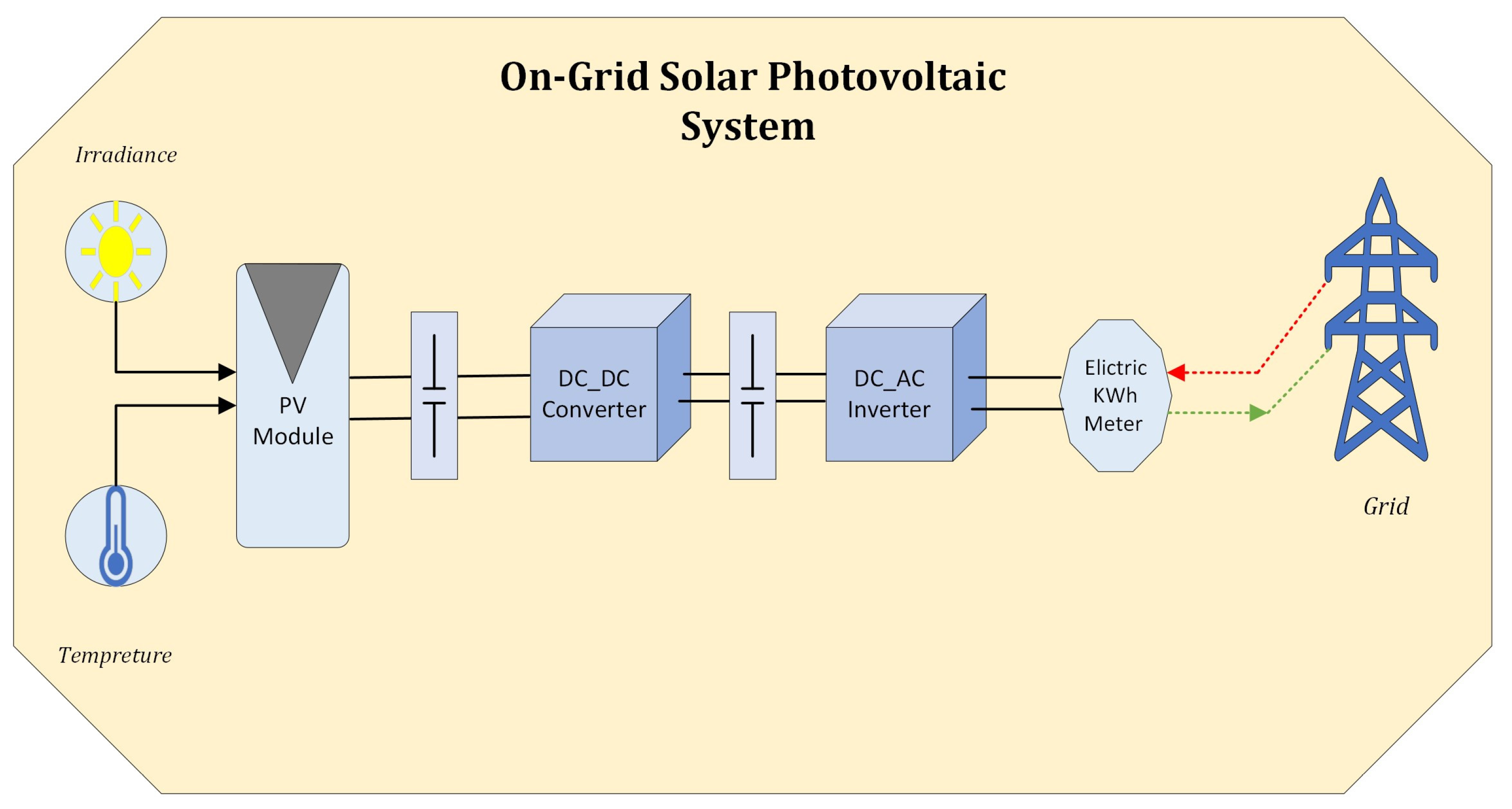
In the last decade, the advancement in power electronic technologies has led the world to redirect the orientation of energy generation to rely on renewable energy sources. A typical residential grid-tied PV system usually consists of Solar PV modules, power electronic DC_DC converters, Battery Energy Storage System (BESS), and grid-interfaced DC-AC inverters.
Figure 1 illustrates an example of a grid-tied residential PV system. Filter circuits are commonly used on the grid side to eliminate the harmonics after the conversion process [
5,
6]. The generated PV power from PV modules flows through DC_DC power converters where maximum power is generated. The main objective of the MPPT controllers is to obtain the maximum power from the PV module and then charge the BESS or pump up the extra power to the grid [
7]. The PV module regularly consists of different groups of PV cells, and a PV module with three submodules (SMs) might be the most common type of PV module. Low-voltage (LV) PV systems can suffer from various faults that negatively affect the performance of the PV system and reduce power generation [
8]. The mismatch issue between the PV modules is one of the most common faults in the PV system, and Partial Shading (PS) can be the most contributing cause to this concern [
9].
The mismatch issues in the PV systems can be categorized into two main groups according to the type of mismatch faults [
10]. Temporary mismatch faults include faults whose effect does not continue with time, and shading can be the main contributing factor to these faults. Although the shading effect can be the most common type of temporary mismatch fault, dust accumulation on PV modules is another serious issue that can adversely affect the amount of generated power from PV systems [
11]. The second type of mismatch issue is permanent faults where the PV system might continue suffering from these types of mismatch faults. Commonly, the permanent mismatch faults can be related to the manufacturing process soldering stage and impurities inside the used materials. However, the PV module’s degradation factor can also be considered a reason for permanent mismatch. The permanent faults can reduce the PV system’s efficiency and reduce the PV system’s output power by 10% [
12].
Increased temperature of the PV module can decrease the performance of the PV system, causing a noticeable reduction in the PV power generation [
13]. The temperature variation can lead to variable current voltage and power voltage curves of the PV modules [
14]. It has been reported in [
10] that changing the PV module temperature results in a noticeable variation in the open circuit voltage of the PV module. Increasing the PV module temperature can cause a clear reduction in the open circuit voltage, minimizing the PV module’s output power. Thus, the behavior of the PV modules will vary according to the operating temperature of each module [
15]. The Maximum Power Point (MPP) of the modules will be different, causing a mismatch issue between the PV modules. In the Standard Test Condition (STC), the temperature of the PV modules is 25 °C; however, in practice, the operating temperatures of the PV modules are different [
16]. The PV modules might suffer from mismatch issues even if they have the same internal specifications and operate under the same conditions except for different operating temperatures.
The PV module performance can be directly proportional to solar irradiance intensity, which determines the power generation from the PV module. The PS results in irregular solar irradiance profiles, which negatively affects the PV system’s output power [
17]. The PS might be uniform shading or non-uniform shading. In uniform PS, the shading can cover the whole PV module, while in the non-uniform PS type, only a part of the PV module becomes shaded. Both types can result in reducing the power production of the PV module [
18]. The shaded part of the PV module behaves differently from the unshaded part. The maximum power of the PV module is determined by the percentage of solar irradiance; thus, a shaded PV module produces lower power compared to an unshaded one. The nature series connection of PV modules leads to the power of the PV system being limited by the PV module, with the lowest power generation causing a mismatch fault between PV modules [
19]. PS occurs due to several reasons, including moving clouds, birds, bird droppings, high buildings, and shading from the trees [
18].
A part of the PV module can experience a higher temperature, creating a hot spot (HS) issue [
20]. The HS effect can be a permanent or short-term effect. The PS might cover part of the PV model for a short time, leading to an increase in the temperature of the shaded part. Once the PS vanishes, the PV module performs normally. However, in some scenarios, the HS might continue to affect the PV module’s performance [
21]. The defects in the PV module during the manufacturing process result in permanent HS, causing mismatch faults between PV cells inside the PV module. This issue can be avoided by a proper monitoring system that can lead to obtaining high-quality PV modules [
22]. The generated power from faulty PV cells can be fewer than normal operating PV cells, which can produce power dissipation in the form of heat. Normal operating PV cells can generate more power compared to faulty PV cells, which produce sink power instead of generating energy. Then, the power will be dissipated in the form of a head. The associated losses due to this fault in the PV module can be more than 5% [
23].
The mismatch problem between the PV modules is one of the main contributing factors to the losses in PV systems [
24]. The series connection of the PV modules is essential for most PV applications to obtain the high voltage output requirement at the grid side. However, it can lead to some issues in terms of performance and power quality of the PV systems. The unequal irradiance profiles are common in most PV system projects, which can result in a significant reduction in PV power production. The behavior of the PV module is usually based on the solar irradiation profiles. Thus, a PV module with a low irradiance level can generate less power compared to a PV module with a high irradiance profile. The nature series connection of the PV modules can lead the PV system to follow the PV module with the lowest power generation, causing a significant power loss to the PV system [
25].
The mismatch problems between PV modules can cause severe issues to the PV system, including HS and reduced power generation; however, bypassing methods are effectively mitigating these concerns. Under the mismatch scenarios, the faulty PV module can generate some power, but it becomes useless using the bypassing approaches since bypassing strategies aim to isolate the faulty PV module from the PV system during a mismatch [
26]. Thus, distributed power electronic methods are proposed to enable the utilization of the maximum available power from PV systems when systems suffer from PS [
27]. Its main objective is to distribute the MPPT technique to a finer level, enabling individual harvesting of the maximum available power from each PV module [
28]. Employing Distributed MPPT (DMPPT) not only mitigates the associated problems of mismatch issues but can lead to utilizing the power from the shaded PV module.
Several strategies have been proposed to overcome the mismatch issue between PV SMs and enhance both the performance and reliability of the PV systems [
29]. The conventional approach to mitigate the mismatch issues between PV SM is bypassing the current and isolating the faulty PV SM from the PV system [
30]. Therefore, the affected PV SM does not pose any concerns to the PV system. The mismatch issue can be mitigated by applying a bypass approach; however, the generated power from the faulty PV SM can be lost. This study aims to individually harvest the power generation from each PV SM, which can be a practical solution to overcome the mismatch issue and obtain the power generation from the affected PV SM.
Shading, temperature variation, and manufacturing tolerance can lead to changing the behavior of the PV components, resulting in different PV components with different power generations being integrated into one system. The PV system can be limited by the PV component with the lowest power generation, resulting in significant power losses. The conventional strategy is applied to overcome mismatch power generation between PV components by integrating a bypass diode and isolating faulty PV components from the PV system. The shaded PV components can generate power, and utilizing the shaded component power can maximize the power generation of the PV system. Distributing the MPPT and employing the power electronic converters can lead to mitigating the mismatch concern and enhance the power generation of the PV system [
31].
The P&O MPPT algorithm is used to obtain the maximum available power from each PV SM inside a PV module. The PV SM voltage is perturbed, and the corresponding power is observed accordingly. This tracking strategy is commonly used in commercial inverters due to its ability to harvest the maximum power from PV components under different environmental conditions. This study employs the P&O strategy to obtain the MPPT from each PV SM [
20].
This paper proposes a three-input single-output micro inverter to mitigate the mismatch issue inside a single PV module. The power generated from a PV cell is relatively low; thus, it cannot be practical to obtain the maximum power from each PV cell. Therefore, obtaining the maximum power from a group of PV cells might be more effective. The PV module is usually divided into groups of cells forming SM, and capturing the maximum power from each group can increase the power generation from the PV system. A cascaded-boost power electronic converter can be a viable solution to overcome the mismatch problem between the PV SMs. Though the cascaded-boost converters might need more passive components, they can improve the power system performance and significantly maximize PV module energy harvesting. The suggested topology aims to harvest the maximum available power from a group of PV cells inside a single PV module. Most PV modules are divided into three SMs; thus, the proposed topology aims to effectively harvest the maximum available power from the three PV cell groups of the PV module.
The control strategy of the proposed topology is based on employing the DMPPT method to harvest the maximum power from each PV SM individually. The local MPPT of the PV SM is applied to perform the MPPT process. Obtaining the maximum power of PV SM is achieved by controlling the output voltage of each single PV SM. In conventional topology, the PS leads to loss of the PV SM power and isolates shaded PV SM from the PV system.
The rest of this paper is structured as follows: The proposed three-input single-output micro inverter topology is presented in
Section 2. The State Space modeling, passive components selection, and controller design are provided in
Section 3. The experimental validation and final discussion are demonstrated in
Section 4 and
Section 5, respectively. The final section summarizes the conclusion of this study.
2. Proposed Distributed Three-Input Single-Output Structure
The PV module commonly has three SMs, which are integrated with a bypass diode to protect the PV module from HS. The shaded SM will be isolated, resulting in the loss of the generated power from the shaded SM. Therefore, replacing the conventional bypass diode with the proper power electronic converter can lead to utilizing the power from the defective SM. The PV module commonly has three PV cell groups; obtaining the maximum available power from each PV cell group can mitigate the mismatch concerns between PV cell groups inside an individual PV module. This paper proposed a new topology to reduce the problem of mismatch between PV SMs inside a single PV module.
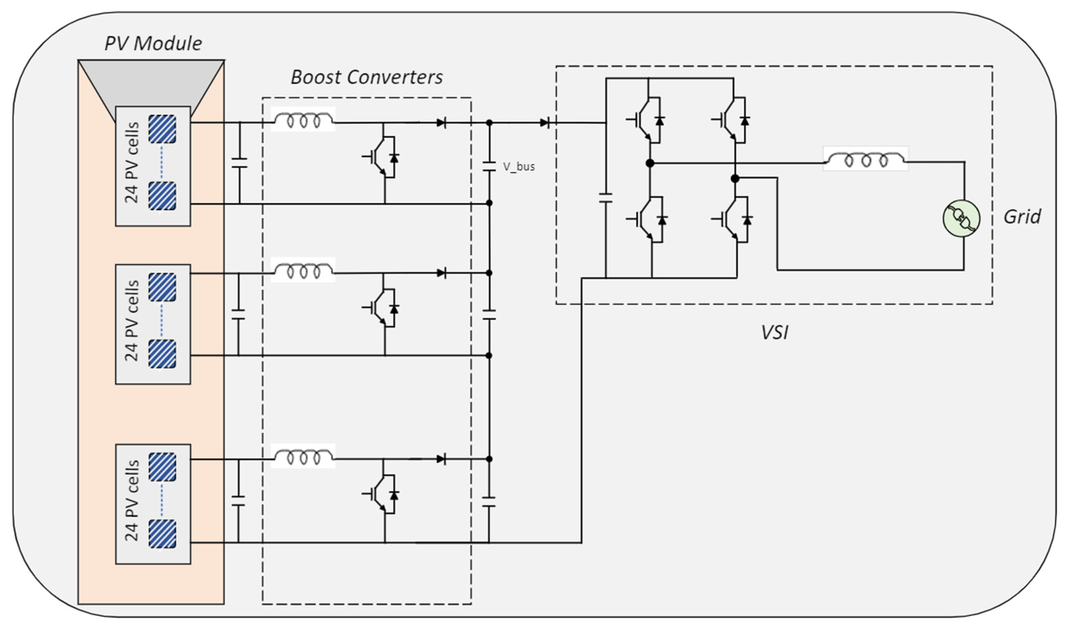
Figure 2 shows the proposed cascaded boost converters used for employing the DMPPT at the PV SM level. The output voltage of the PV SM can be relatively low, and the boost converter has a limited boosting range for voltage output; therefore, the output of the three boost converters cascaded to enhance the boosting-up capability of the proposed topology. A Voltage Source Inverter (VSI) is used on the grid side to convert the PV DC power to AC power at the utility. The cascaded topology is linked to the utility grid via a forwarding diode to protect the PV side from reverse currents during a faulty system. A DC link capacitor is employed between the PV side and grid side to provide a decoupling function and mitigate the Total Harmonic Distortion (THD) effect grid [
32].
The nature of PV power is changeable due to different climate conditions, which can change the PV subsystem’s power generation. The PS is a continuous challenge in PV systems because it results in a massive reduction in power production and can lead to unavoidable drops in the output voltage. One of the most proper methods to reduce the negative impact of unbalanced power generation caused by different irradiation levels on the PV system is based on dividing the entire PV system into subsystems. It would be ideal if each PV cell could be handled individually; however, that can result in a significant increase in the installation cost, and it will require a complicated controlling system. Therefore, extracting the maximum power from a group of PV cells can be more practical. The PV cells are commonly grouped into three or four groups inside a single PV module, and each group of PV cells is integrated with a bypass diode to reduce the impact of partial shading. The bypass diode will allow the current to flow through it, resulting in the loss of the power generated from a shaded group of PV cells. The main objective of the suggested topology is to utilize the power from the affected group by individually harvesting the maximum power from the PV SM.
Several PV modules are usually integrated, forming the residential PV systems according to the local load of the end users. The proposed structure aims to mitigate the mismatch concern at PV SM inside a single PV module, which can lead to mitigating the root of the mismatch concerns. Increasing the size of the PV system will not pose an issue since the mismatch problem is targeted at the PV SM level.
Protecting the PV module is considered during the design stage of the proposed topology. The integrating diode between the PV module side and the grid side aims to block the reverse current flows into the PV module. This can maintain the stability of the suggested system and maintain normal operation of the PV system.
3. State Space Analysis of Proposed Converter to Design System Controllers
Modeling by averaging [
33] is a common, effective method to model the switched power converters in power electronics. It aims to average the model over one switching cycle to overcome the nature of switching power converters. Power electronic systems are commonly nonlinear, and modeling nonlinear systems can be a complicated process; thus, linearizing these types of systems around one operating point can solve the nonlinearity issue. After obtaining the linearized model, the system state variables are perturbed by small values to obtain the small signal model. This model is usually effective and can mimic the actual model’s dynamic behavior. The derived small signal model of the boost converter using this strategy is used in this study.
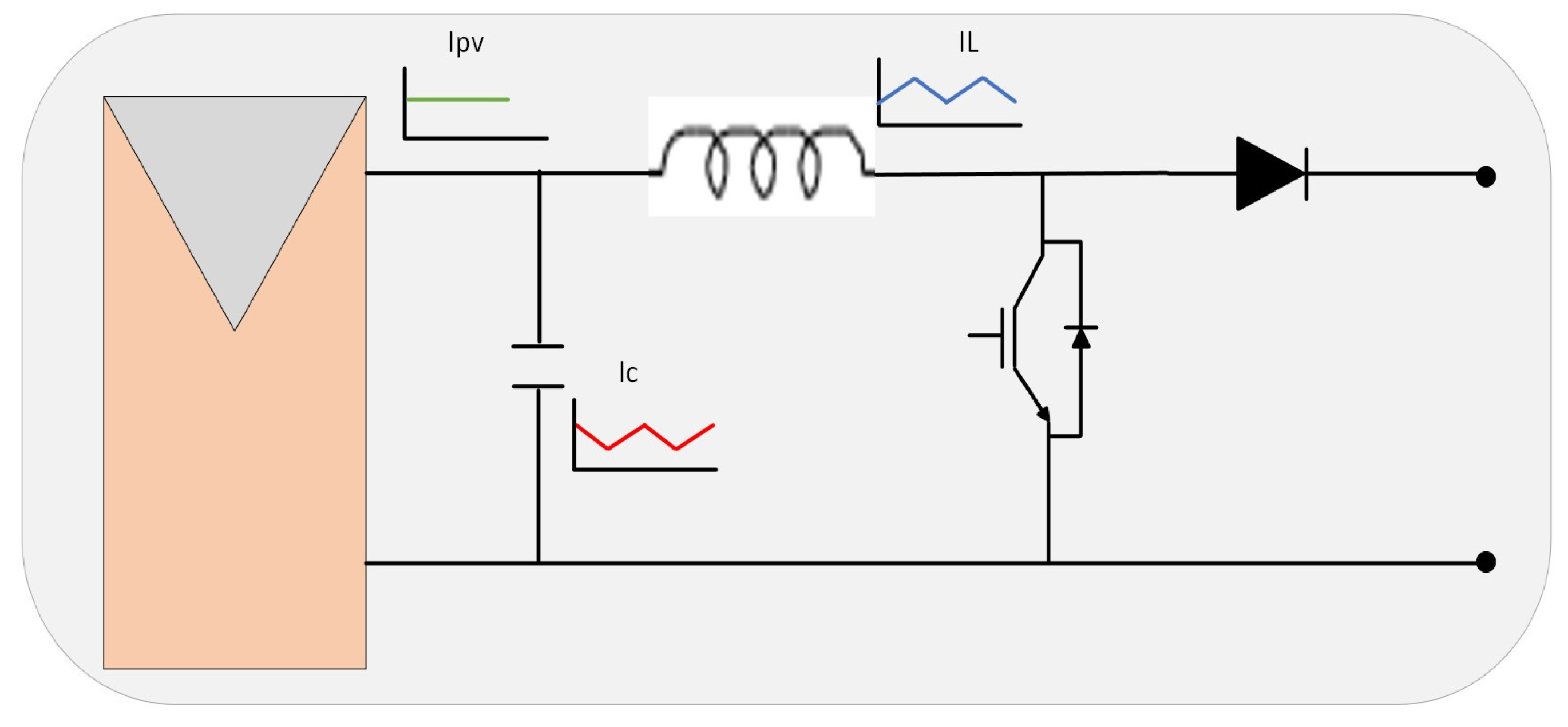
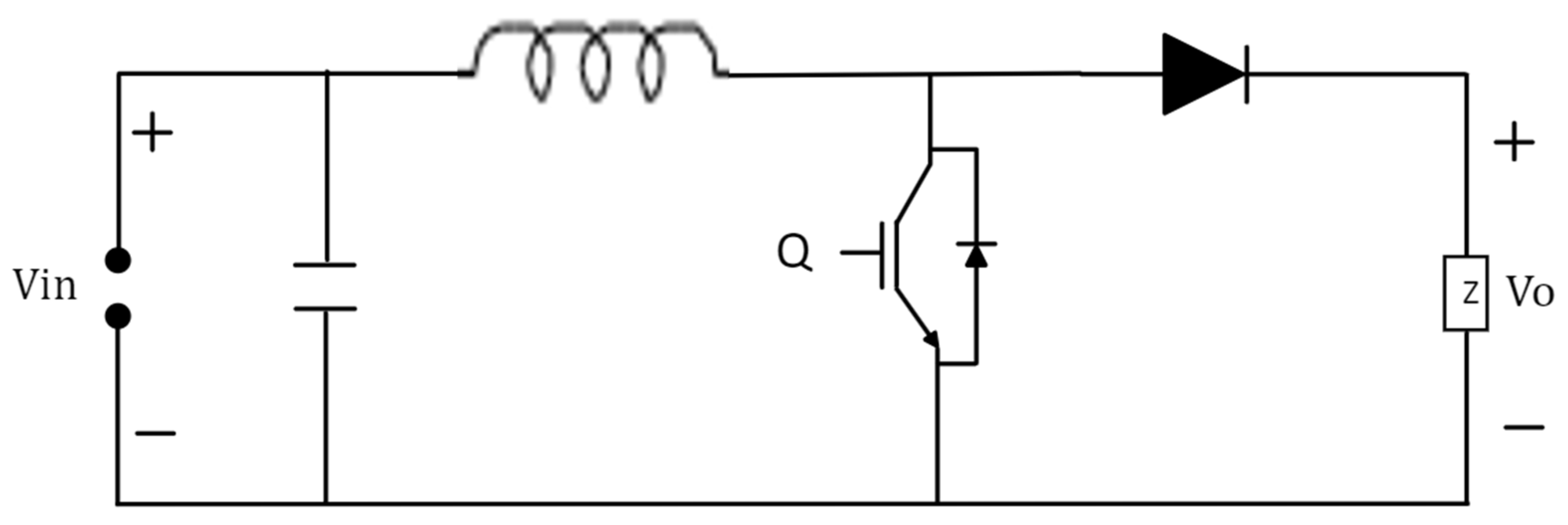
The boost converter module is based on the circuit shown in
Figure 3. The converter component is assumed to be ideal, and the component’s internal losses are neglected. The system equations are obtained using the general averaging method as follows:
When the switch Q is turned on, the state equation becomes
When the switch Q is turned off, the state equation becomes
After obtaining the state space equations of the boost converter, the ON and OFF state matrices become as follows:
The following equations are used to obtain the averaged model:
To calculate the steady state values
and
, the equation below can be used:
A small perturbance is applied to the state variable to obtain the small signal module where ~ represents the small perturbation to the variables:
After calculating the new
and
matrices, the transfer function can be obtained using the following equation:
3.1. Passive Component Selection
The proposed topology employs the boost converter since the output voltage of the PV SM is relatively low. In such a converter, the output voltage will be higher than the voltage at the MPP. The input voltage from the PV SM might be obtained under the maximum irradiation level condition. Each PV SM is assumed to operate at the maximum available power; thus, the PV SM voltage will be represented by
. According to the steady-state analysis, the duty ratio at the output voltage of each submodule might be expressed as follows:
where
δ is the duty cycle;
is the output voltage of each boost converter, and
is the corresponding voltage at MPP.
The input inductor value of the boost converter can determine the input current ripples. Obtaining the right value for the inductor of the boost converter can be calculated during the rising state when the boost converter’s switch is turned on. Under the assumption of constant input current from the PV SM, the capacitor current will be expressed by subtracting the PV SM input current from the boost converter inductor current. The waveform of the inductor current of the boost converter is assumed to be triangular; thus, the capacitor current will have the antiphase triangular waveform. Integrating the triangular area can equal the amount of charge stored in the capacitor.
Figure 4 illustrates both the circuit and current waveforms of the PV SM boost converter. In a grid-tied inverter, the
DCBUS capacitor value is selected according to the input and output power to buffer the second-order harmonic distortion of the proposed structure, and current-based derivation can be used to obtain the most proper value for the
DCBUS capacitor. Proper selection of capacitor value can maintain pure DC power from the PV input and sinusoidal waveform current at the grid side. In the same concept, the
DCBUS capacitor value can be selected with the assumption that a pure DC flows from cascaded boost converters. The grid current waveform shape is sinusoidal, which means the current flowing through the capacitor will be the same as the grid current; however, the capacitor current sign will be reversed in direction.
The parameter of the proposed boost converters will be selected according to Continuous Conduction Mood (CCM) as follows:
The design of the proposed three-input single-output power electronic converter can be expressed by calculating the output voltage of the common DC bus. The three-output voltages of the cascaded boost converters are added to express the output voltage at the DC bus, where n is the number of PV SM.
3.2. Open-Loop Analysis and System Dynamic Investigation
After obtaining the transfer function of the boost converter, the values of
L,
, and
are calculated according to the CCM and with the assumption that the system has balanced energy operation; the values of the system are illustrated in
Table 1. The obtained small signal averaged module of the boost converter shows two poles and a nonnegative zero. In order for the system to achieve internal absolute stability, the two poles have to be on the left-hand side of the s-plan. The non-negative zero can result in a reduction in the phase margin and cause undershoot during transient time; however, zero cancelation can negatively affect the overall stability of the system.
The voltage and current values at the MPP of the PV SM boost converter are selected according to a typical PV module. In terms of the design of the passive component of the boost converter, during the ON state of the boost converter, the inductance can be calculated according to the peak-to-peak ripples of the inductor current, and the selected inductor value of the PV SM boost converter is calculated considering small peak-to-peak ripple value. The output capacitor of the PV SM boost converter is selected after a compromise between the capacitor value and peak-to-peak ripples at the voltage output.
Thus, the most proper method to minimize the effect of the non-negative zero is trying to make it faster by locating it far from the origin (0,0) since faster zeros are less harmful than slower ones.
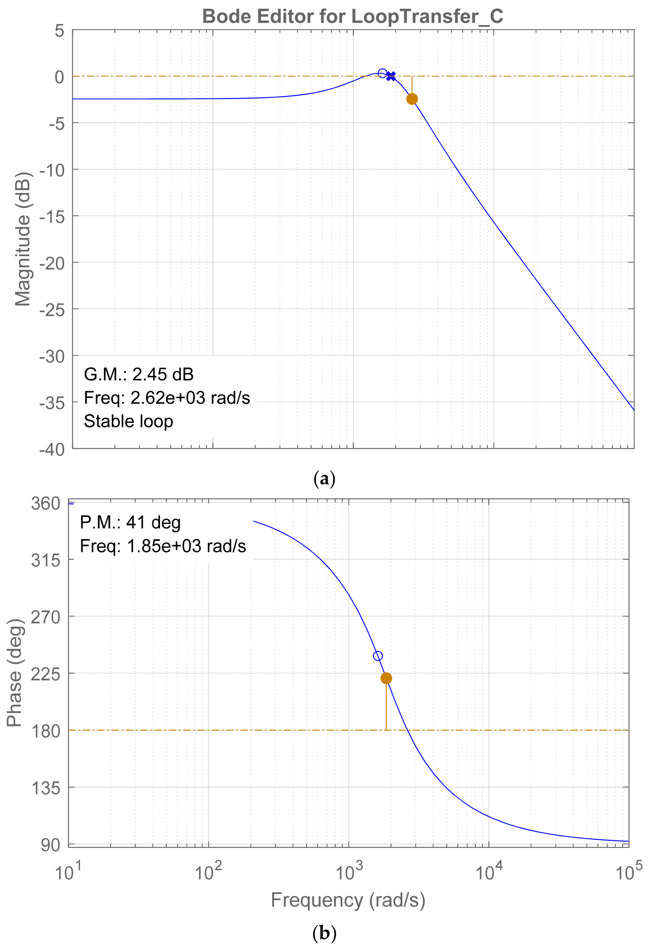
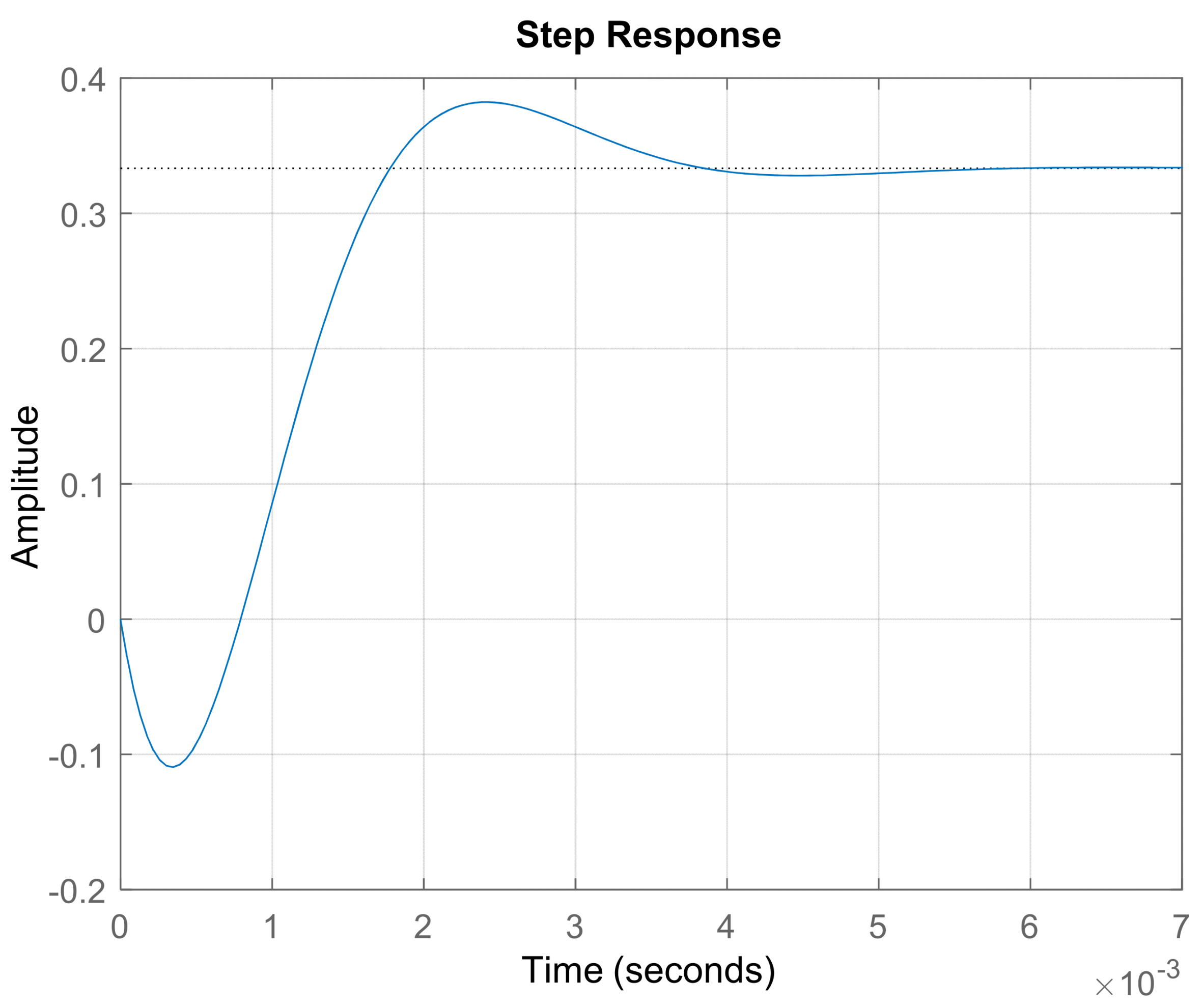
Figure 5 shows the Bode plot of the boost converter without controllers, and the frequency response illustrates that the system is stable, and both the gain margin and phase margin are positive numbers. However, the systems seem critically stable since the gain margin is close to the negative region. The step response of the boost converter is illustrated in
Figure 6, which shows a noticeable undershoot during transient time, which results from the non-negative zero of the boost converter transfer function. A proper controller should be selected to overcome this issue and shift the system to a stable region.
3.3. Closed Loop Analysis and Design of the Controller for Proposed Structure
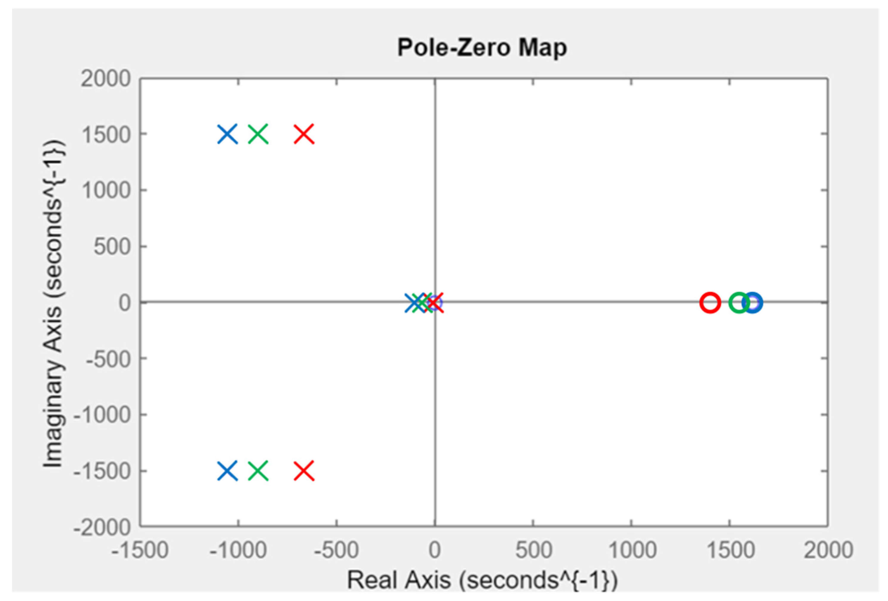
The obtained open-loop system has two complex poles at −261 rad/s and one positive zero at 1610 rad/s. From control theory, the system stability is directly related to the pole position of the system. Enhancing the system stability is usually related to the capability of the controller to shift the poles to the left-hand side. The positive zeros usually do not lead to total loss of stability of the system; however, they can pose serious issues like a large undershoot and minimizing the phase margin of the system. A common strategy to minimize the negative effect of the positive zeros on the systems is trying to make the zeros fast. Fast zeros are the zeros that are located far from the origin (0,0). The fast zeros have low negative effects compared with slow ones. The SISO tool in SIMULINK/MATLAB has been used to obtain and tune the parameters of the controller of the proposed system. The compensator improves the system’s stability and gives better performance by shifting the system’s poles to the stable side LHS.
The poles and zeros for the parameters illustrated in
Table 1 are plotted in
Figure 7. The
ki gain of the controller is fixed to 0.6, while
kp varies from [0.2 to 0.5] to study the proposed system dynamics. The 0.25 gain of the
kp parameter of the PID controller can provide the most proper dynamic response to the system. The SISO tool in SIMULINK/MATLAB has been used to obtain and tune the PR controller parameters, and the result illustrates that the most proper
kp and
kr gains of the PR controller that achieve appropriate stability and appropriate bandwidth are 3 and 5, respectively.
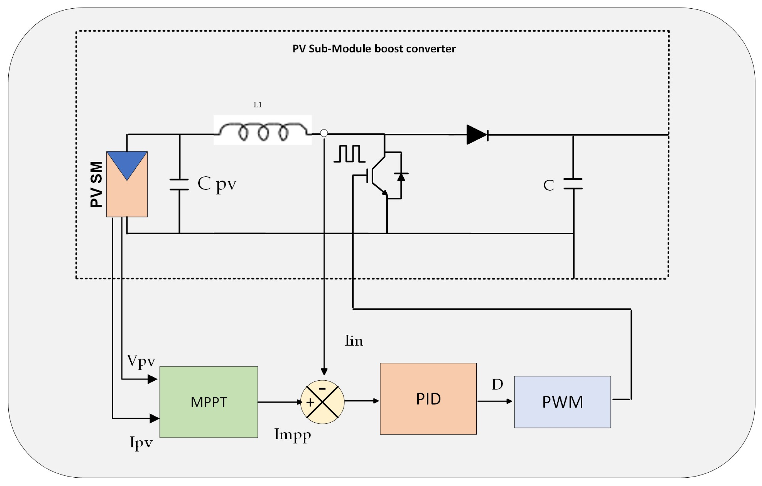
The Proportional Integral Derivative (PID) controller is one of the most commonly used controllers for power electronic converters, and it has been used for the input side of the proposed structure. The proposed controller will determine the current at the maximum power point at a specific temperature and irradiation level. This current is obtained as a reference current for the controller, which will be compared to the actual inductor current of the boost converter. The error between the two current values of each boost converter will be controlled by a PID controller. The purpose of the controlling process is to keep the input current from the PV submodule flat DC with minimal ripples, which can lead to a more accurate tracking process.
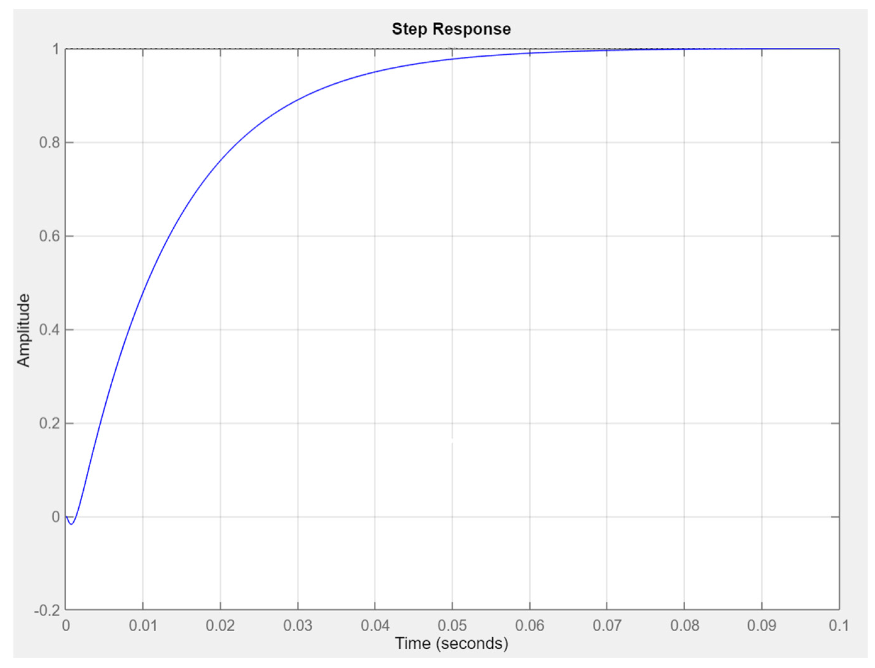
Figure 8 illustrates the improvement in the dynamic system response and the step response characteristic when applying the proper controller to the system.
The proposed closed-loop input current controller at the PV submodule is shown in
Figure 9. I
MPP drives the subsystem input controller at the submodule level. The compensator aims to regulate the DC from the input current and mitigate the negative effect of the second harmonics of grid frequency. Eliminating or reducing the second harmonics distortion from the PV side can improve the performance of the maximum power point tracking algorithm and improve the PV system efficiency. The MPP tracking system calculates the I
MPP of the submodule according to the irradiation level and temperature; if this current is used as a reference input of the compensator, then it will be compared to the actual input current of the boost converter to perform the controlling process.
The total output voltage from the inverter side of the proposed system can be expressed as follows:
where
V is the voltage amplitude of the vs., the
Vg is defined as the magnitude of the grid voltage and * represent the reference value of grid current. If the proposed system injects an active power
P to the grid at the power factor cos(
α), the single-phase output current can be expressed as follows:
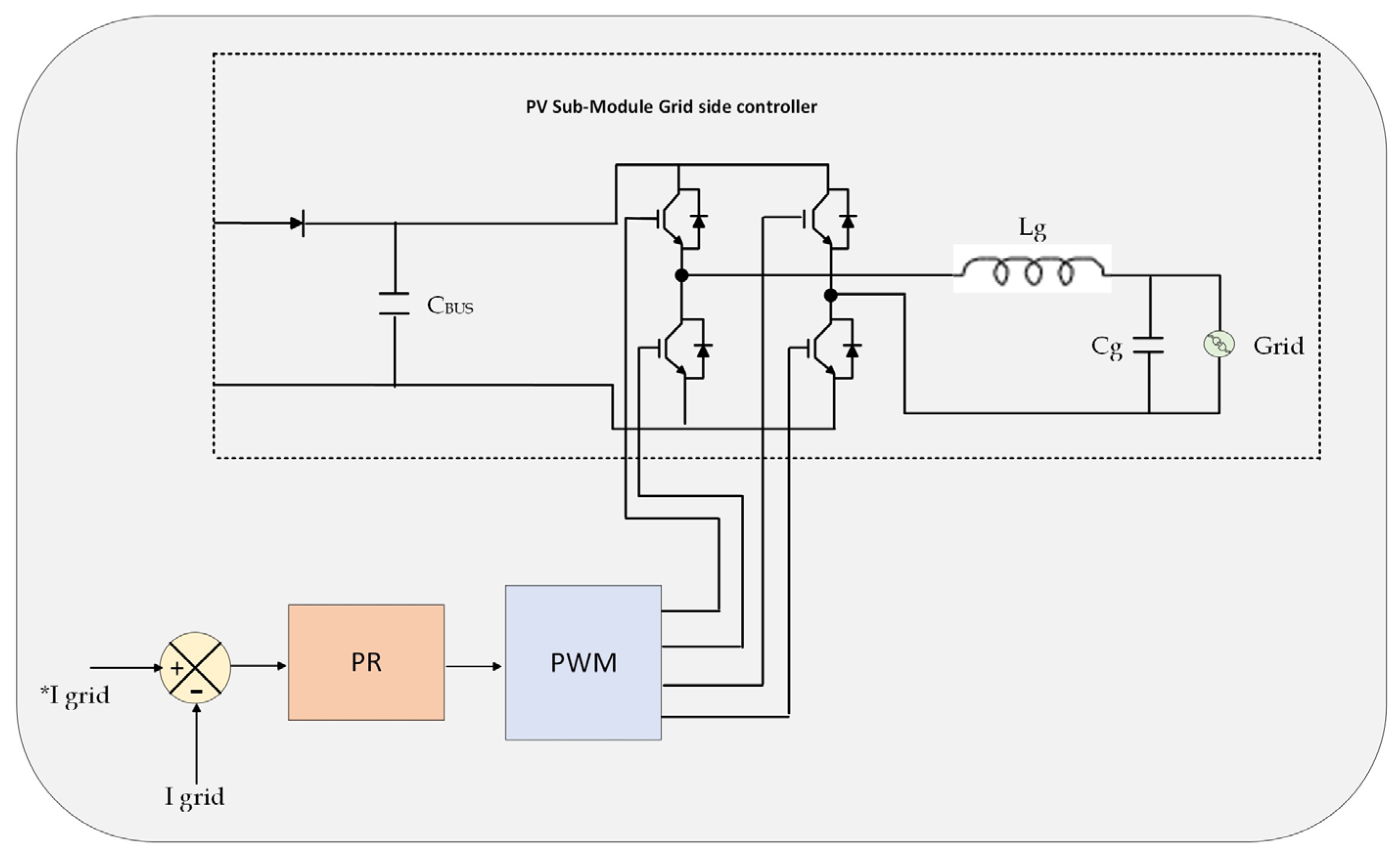
Usually, controlling the alternating current is based on converting the alternating current to constant values and then performing a controlling process by a conventional PID controller and converting it back to controlled alternating signals. This strategy has been used for years, and it can be appropriate for several applications; however, it requires several design stages, which might affect the performance of the controlling process. The Proportional Resonant (PR) controller has been used in several applications to control alternating signals, and its validity has been proven. The PR controller is used in this study to control the grid current to maintain a sinusoidal current waveform at the grid side. The controlling strategy used in this study is based on sensing the grid current and comparing it with the desired value to calculate the error between the two signals. This will pass through the PR controller, which performs the control process and tracks the sinusoidal referenced grid signal. The block diagram of the controller for the proposed topology is illustrated in
Figure 10.
The PR controller Laplace transformation is
where
is the proportional gai;
and
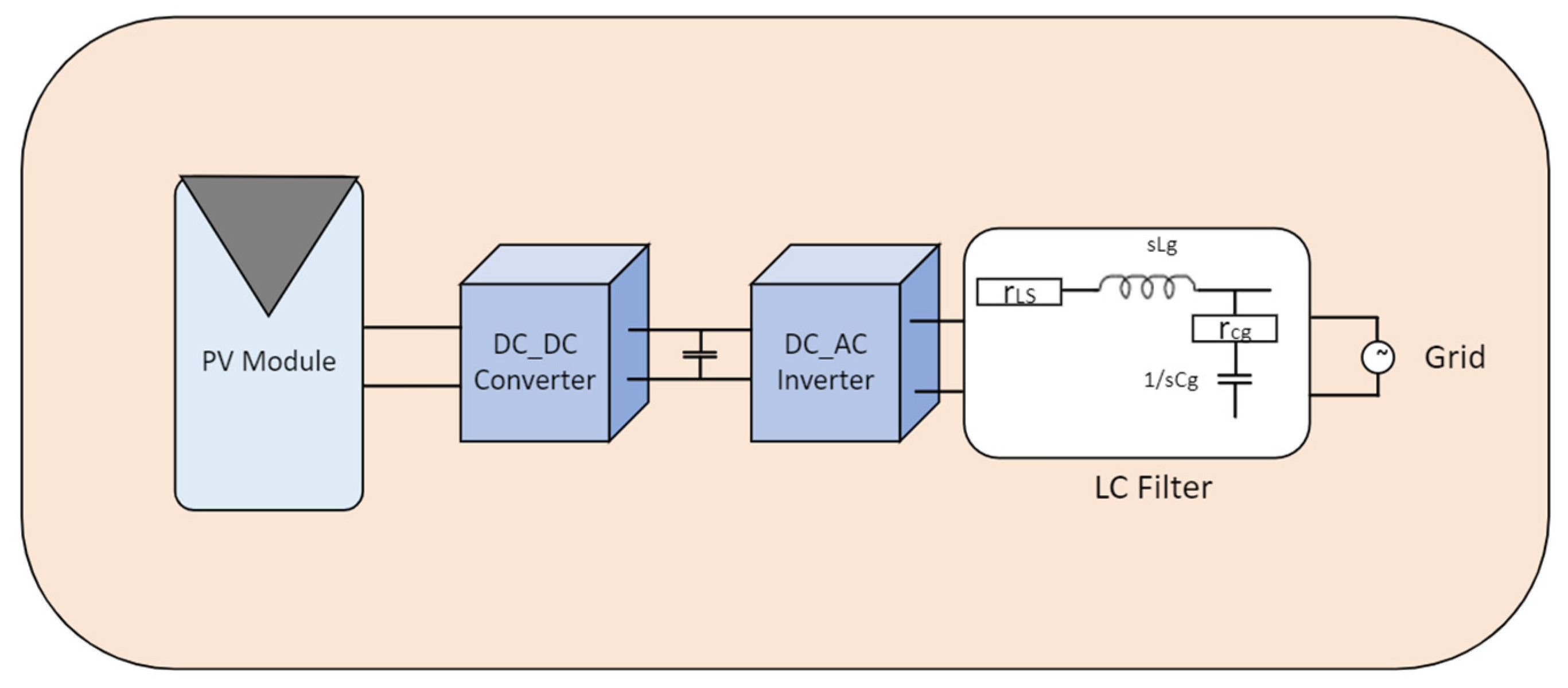
are resonant gain and frequency, respectively. The conventional PID controller is suitable for systems with constant values, such as DC-DC converters, and it can eliminate steady-state errors and provide fast response. However, the PID controller cannot track sinusoidal waveforms. The PR controller can provide an infinite gain at a selected frequency; thus, it is commonly used in grid-connected inverters. The grid side of the proposed system can be represented by an LC filter, as illustrated in
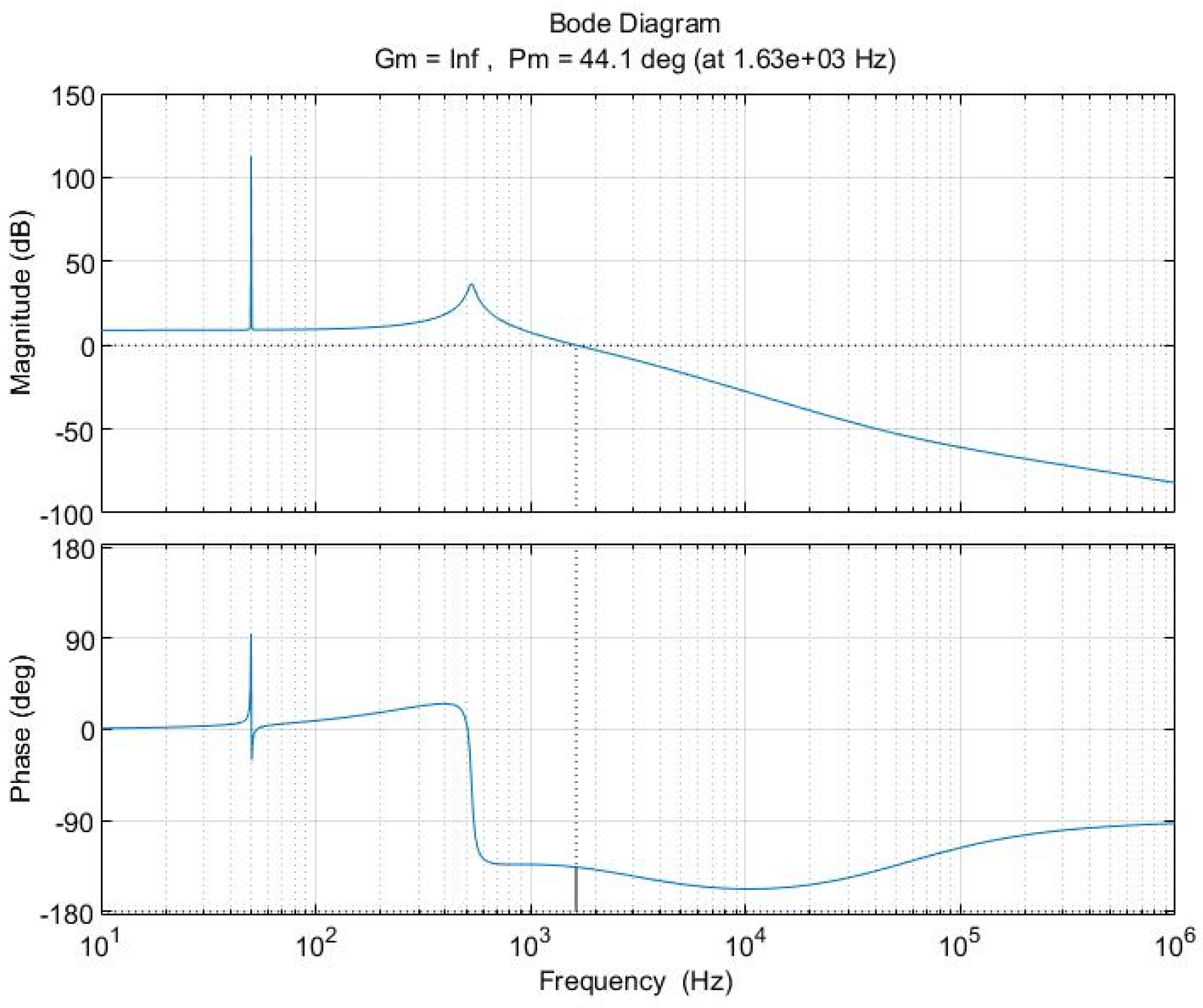
Figure 11. The bode plot of the PR controller used in this study is shown in
Figure 12.
The Laplace transfer function of the LC filter is given by the following equations:
4. Experimental Results
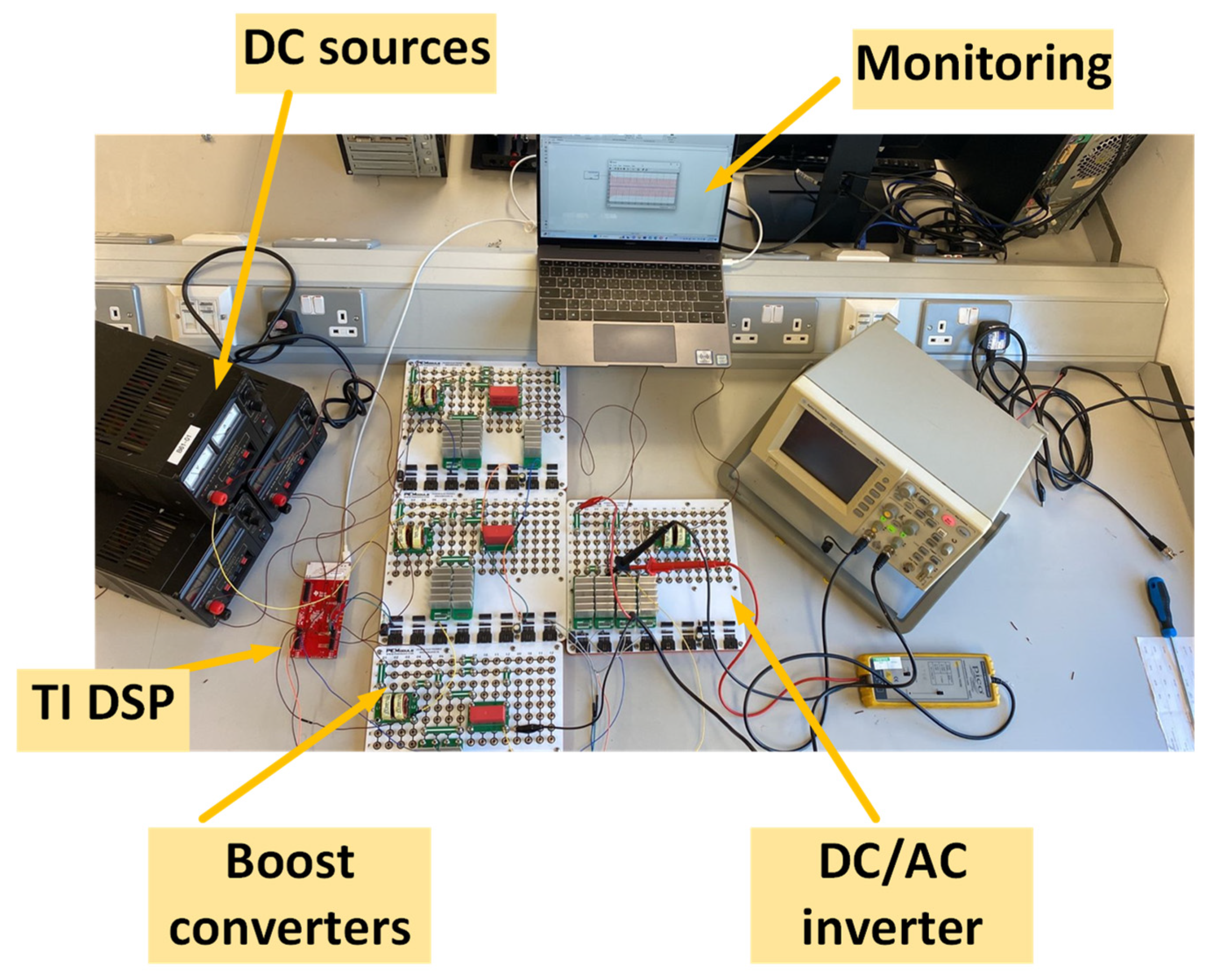
The experimental setup for obtaining the maximum available power from the three SMs inside an individual PV module is shown in
Figure 13. Each PVSM is rated at 250 W; thus, the maximum available power from a PV module is rated at 750 W. The system is controlled by the Texas Instrument Digital Signal Processor (TMS320F28335), which is used to control the gate signals for the three boost converters at the input side. DC power supplies are used to mimic the PVSM. The PV module output is linked to the utility grid through an autotransformer, which steps down the grid voltage from 240 V to 100 V. The three PV SMs are connected to three separate DC power sources, mimicking the PV module. The output DC power from the PV module is inverted to a Low Voltage AC grid (LV AC) to examine the validity of the proposed topology.
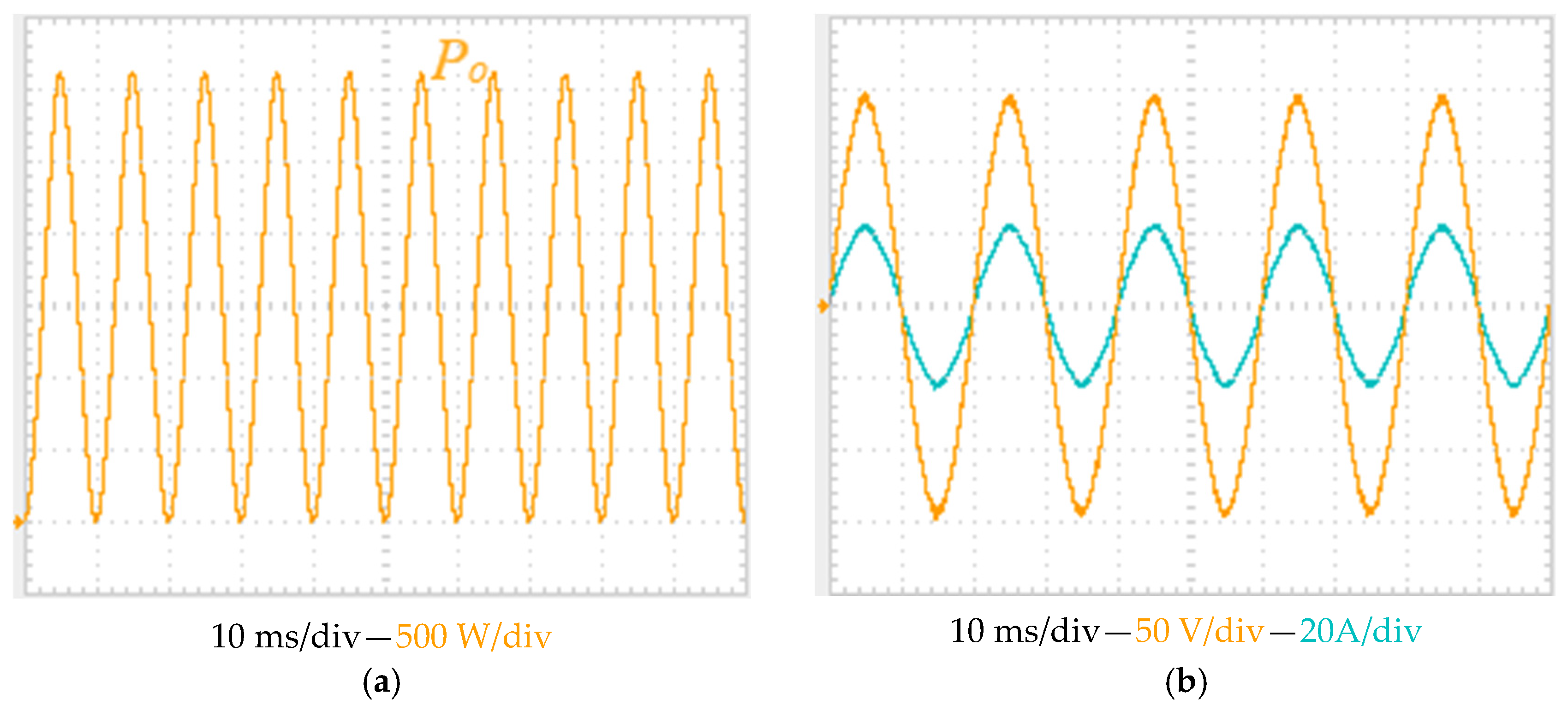
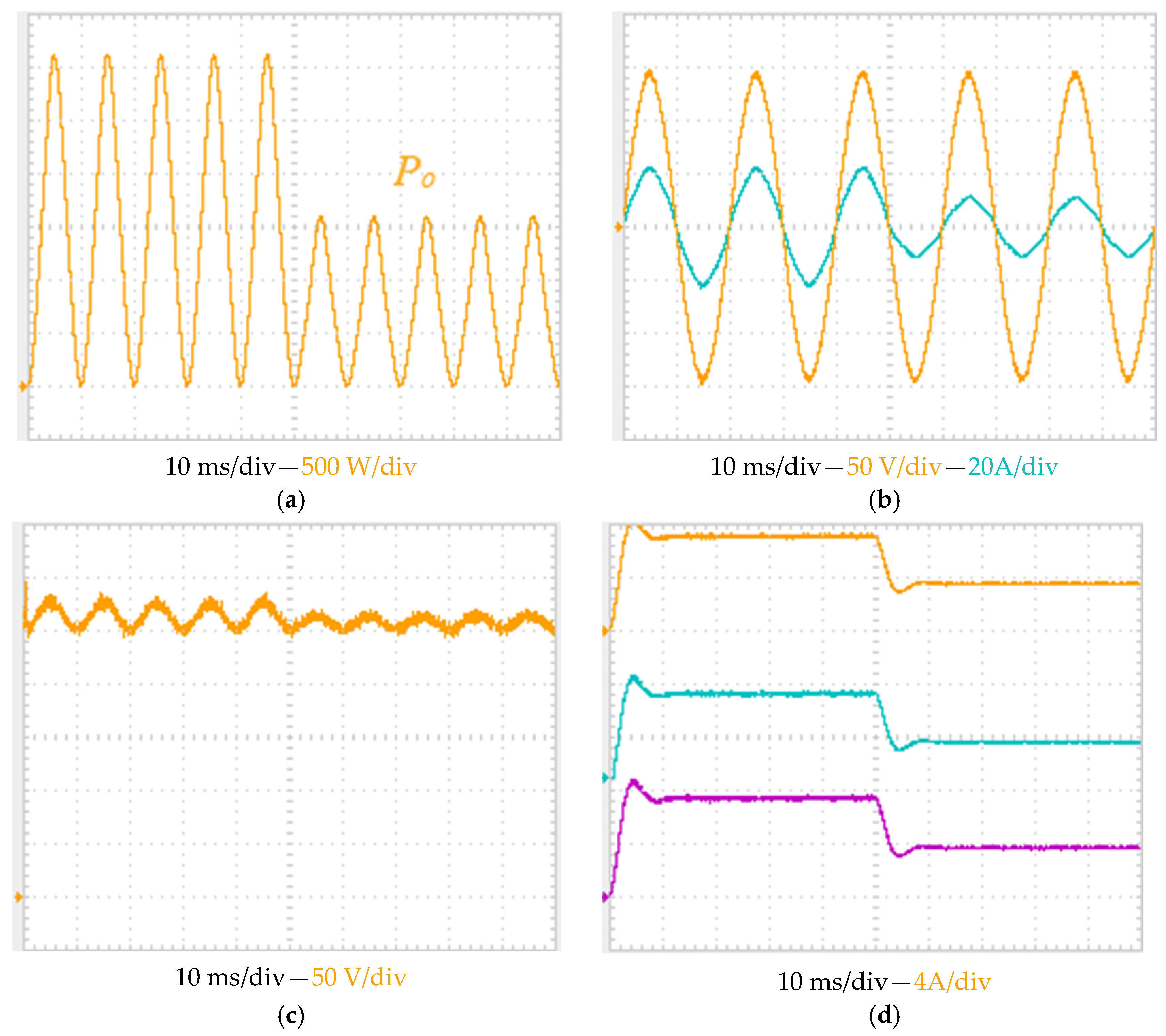
The experimental results of the suggested topology for employing the DMPPT at the PVSM level are shown in
Figure 14.
Figure 14a shows the total input power of the system.
Figure 14b shows the output voltage and current when the power is injected into the grid through the autotransformer at unity power factor.
Figure 14c shows the DC-link voltage between the PV SMs and the DC/AC inverter. Finally,
Figure 14d shows the input currents of the PV SMs.
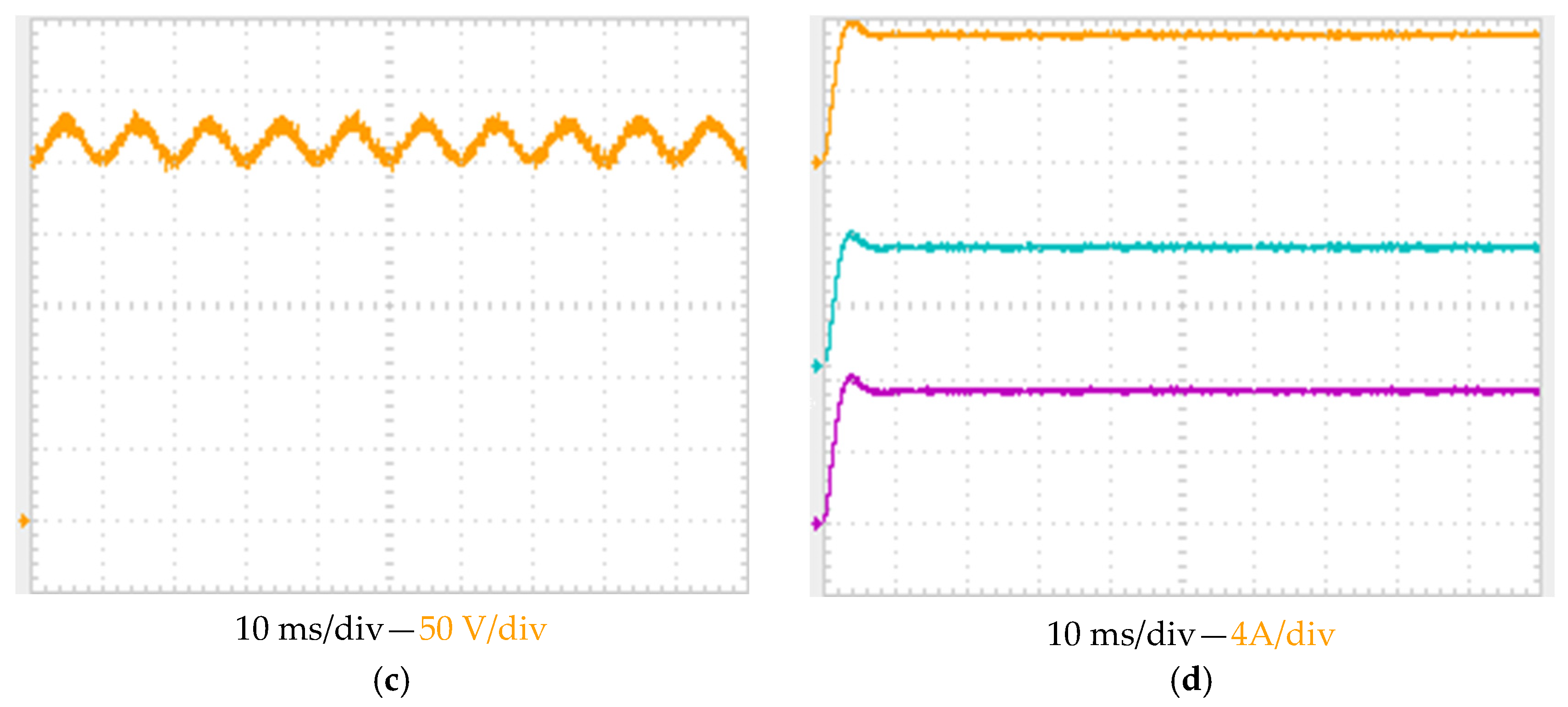
The stability of the proposed system is examined by suddenly dropping the output power of the system by 50%.
Figure 15 shows the response of the grid current to variation in the output power, resulting in a decrease in its maximum value. Also, the input current of the three SMs is dropped as a result of decreasing the output power of the system.
The results illustrate that applying the MPPT at PV SM can lead to harvesting the available power from each group of PV cells individually. Thus, the amount of power generation from each PV SM is directly related to the irradiation level. Unlike the conventional strategy where shaded PV SM is isolated from the PV system, the suggested topology aims to obtain the available power from PV SM, regardless of the amount of power of the other two PV SMs.
5. Discussion
The PS and mismatching concerns can result in a great reduction in the power generation of an individual PV module. These issues are unavoidable in most scenarios and can affect the performance of the PV system. It has been proven that distributing the MPPT system can achieve higher power generation and mitigate the problem of mismatch. The output voltage of a single PV cell is relatively small, and cascading several PV cells is required to obtain a higher output voltage. This strategy can solve the low voltage problem of a PV cell; however, under the PS effect, the power generation of the PV system is reduced.
The series connection of PV cells results in different power generation under the existence of the PS problem. Obtaining the power generation from each PV cell needs a complex control system and maximizes the system cost. Three or four strings of PV cells are commonly connected, forming a PV module. The conventional method to tackle the mismatch issue between the solar cell strings is to integrate a bypass diode with each PV cell string. The result is isolating the shaded PV cell string from the system and allowing the PV module current to pass through the bypass diode. Isolating a part from a PV module means that the generated power from an isolated solar cell string is lost.
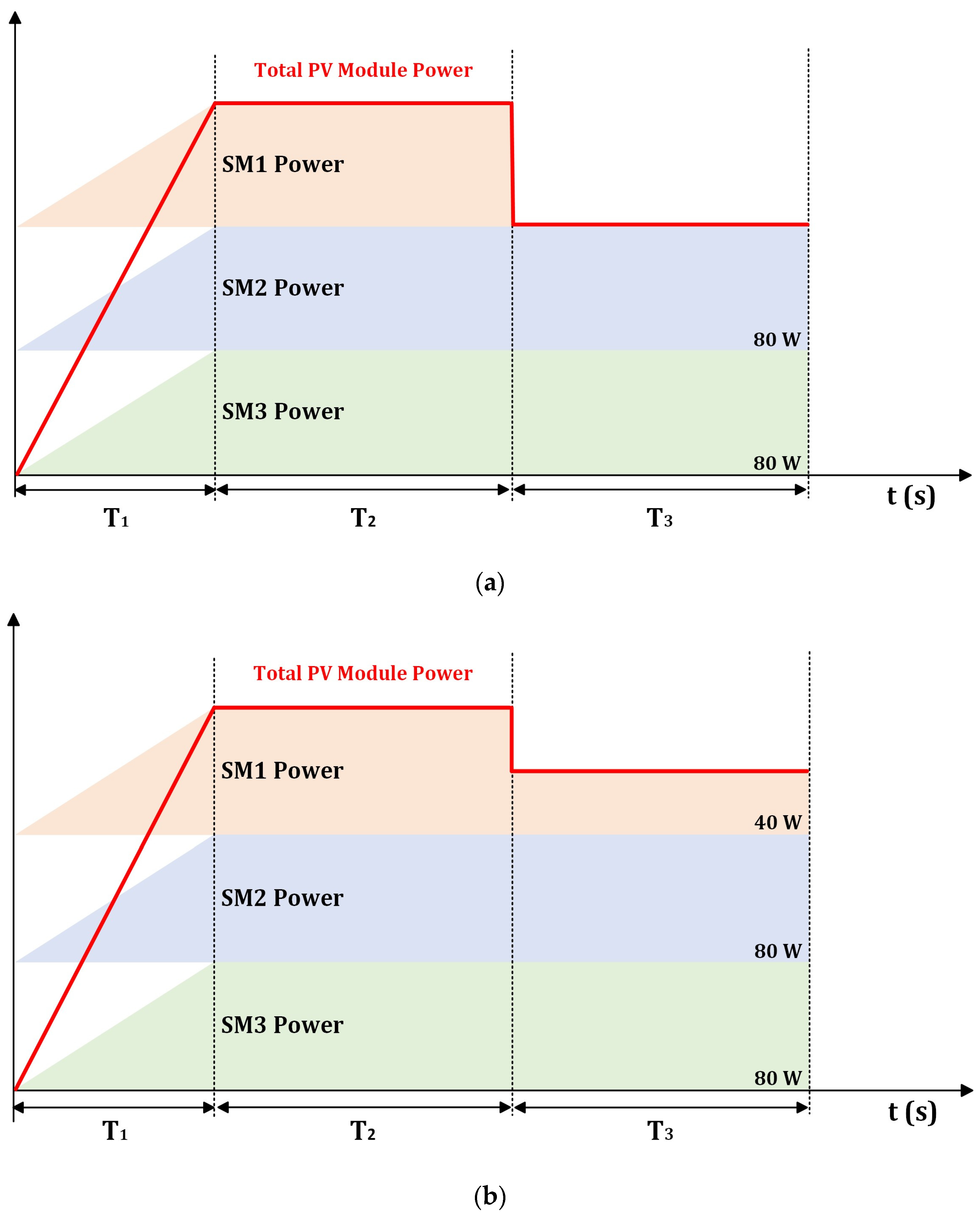
Figure 12 illustrates how the proposed distributed power converter can contribute to maximizing the PV module power generation.
The power generation for the proposed topology is illustrated in
Figure 16 and demonstrated in the following manner. In the initial stage, at T1, the power generation of the three-PV SM is equally likely, starting from zero and gradually increasing to reach maximum power At T2. The power of a single-PV SM is 80 W; thus, the total power of a PV module is 240 W. In the subsequent period, the PS covers one PV SM. In the conventional method, the power generation from shaded PV SM is lost. However, in the suggested topology, power generation will be harvested individually, resulting in utilizing the power from shaded PV SM.
The presented structure aims to harvest the power from the shaded part of the PV module instead of isolating it from the PV module by employing a power electronic boost converter with each SM. The purpose of the boost converter is to obtain the maximum available power from each PV cell group. Boost converter has been chosen due to its capability to step up the low voltage at the PV SM side. Although the boost converter is designed to boost the input side voltage to a higher voltage at the output side, its boosting capability is limited to a specific output range. The output voltage of boost converters is connected in series to meet voltage requirements at the utility grid. Also, the proposed topology is designed to harvest the maximum power from the PV side with DC to AC inverting capability.
The proposed topology targets the future residential PV system since the existing Grid-connected system uses conventional PV modules where PV SMs are integrated with bypass diodes. Prototypes for PV cell optimizers have not yet been produced; however, related companies have started applying the Distributed MPPT on the PV SM.


