Article

High-Q Terahertz Perfect Absorber Based on a Dual-Tunable InSb Cylindrical Pillar Metasurface

by
Rafael Charca-Benavente
1,
Jinmi Lezama-Calvo
2 and
Mark Clemente-Arenas
2,*
1
School of Electronic Engineering, Universidad Nacional de San Agustin de Arequipa, Arequipa 04000, Peru
2
Electronics Circuits and Systems Research Group gECS-HF, Universidad Nacional Tecnológica de Lima Sur UNTELS, Villa El Salvador, Lima 15834, Peru
*
Author to whom correspondence should be addressed.
Telecom 2025, 6(3), 70; https://doi.org/10.3390/telecom6030070
Submission received: 27 July 2025 / Revised: 1 September 2025 / Accepted: 8 September 2025 / Published: 22 September 2025

Abstract

Perfect absorbers operating in the terahertz (THz) band are key enablers for next-generation wireless systems. However, conventional metal–dielectric designs suffer from Ohmic losses and limited reconfigurability. Here, we propose an all-dielectric indium antimonide (InSb) cylindrical pillar metasurface that achieves near-unity absorption at f 0 = 1.83 THz with a high quality factor of Q = 72.3 . Critical coupling between coexisting electric and magnetic dipoles enables perfect impedance matching, while InSb’s low damping minimizes energy loss. The resonance is tunable via temperature and magnetic bias at sensitivities of S T 2.8 GHz · K 1 , S B TE 132.7 GHz · T 1 , and S B TM 34.7 GHz · T 1 , respectively, without compromising absorption strength. At zero magnetic bias ( B = 0 ), the metasurface is polarization-independent under normal incidence; under magnetic bias ( B 0 ), it maintains near-unity absorbance for both TE and TM, while the resonance frequency becomes polarization-dependent. Additionally, the 90% absorptance bandwidth ( Δ f A 0.9 ) can be modulated from 8.3 GHz to 3.3 GHz with temperature, or broadened from 8.5 GHz to 14.8 GHz under magnetic bias. This allows gapless suppression of up to 14 consecutive 1 GHz-spaced channels. This standards-agnostic bandwidth metric illustrates dynamic spectral filtering for future THz links and beyond-5G/6G research. Owing to its sharp selectivity, dual-mode tunability, and metal-free construction, the proposed absorber offers a compact and reconfigurable platform for advanced THz filtering applications.

Graphical Abstract

1. Introduction

Millimeter-wave (mmWave) operation in 3GPP Release 17 extends 5G NR beyond the original 52.6 GHz limit [1]. Looking ahead, the wireless-research community foresees sub-terahertz (100–300GHz) and terahertz (0.3–10 THz) carrier frequencies as a cornerstone of sixth-generation (6G) systems, promising fiber-like data rates, centimeter-level localization accuracy and joint sensing–communication capabilities [2,3,4]. Delivering those benefits demands passive components like filters, absorbers, and detectors that can manipulate THz waves with sub-gigahertz resolution while remaining compact, low-loss, and tunable.
Perfect absorbers (PAs) convert incident radiation into heat with nearly 100% efficiency, eliminating reflections and transmissions at a designated resonance. The PA by [5] combined electric and magnetic split rings on a metal ground plane, achieving unity absorbance in the microwave regime. When scaled to THz, however, such metallic architectures suffer excessive Ohmic loss, limiting their loaded quality factors to Q 10 [6]. Replacing metals with high-index dielectrics unleashes much sharper lineshapes. All-dielectric metasurfaces supporting quasi-bound states in the continuum (quasi-BICs) have recently reached Q > 1000 together with near-unity absorbance in the range of 0.4–0.9 THz [7]. Yet most high-Q dielectric absorbers remain static; active tuning is typically added by overlaying graphene sheets or phase-change films, which re-introduce loss and fabrication complexity [8,9].
Narrow-gap indium antimonide (InSb) offers a compelling monolithic route to tunability. Its bulk plasma frequency naturally falls in the THz band, and its free-carrier density, and therefore, permittivity, can be modulated thermally or with a modest static magnetic field through the magneto-Drude effect [10,11]. Thermally tunable InSb metasurface absorbers have demonstrated frequency shifts of 2 4 GHz · K 1 at 1–2 THz but with only moderate quality factors ( Q < 30 ) [12]. Magnetically controlled counterparts have reported sensitivities of about 16 GHz · T 1 and high Q-factors around 200, although they often rely on multiple tunable materials to achieve such performance [13]. Moreover, most existing devices rely on multilayer patterning or exhibit polarization sensitivity, which are undesirable for large-scale, wafer-level fabrication.
Beyond intrinsic InSb, structurally similar THz absorbers have been realized with other active media. Phase-change V O 2 metasurfaces offer large on/off contrast and thermal switching near 68 °C, but they exhibit first-order transition hysteresis and added loss, which can limit continuous tuning and stability [14,15]. Graphene-based absorbers provide rapid, reversible electrical control via Fermi-level gating, yet near-unity absorption typically relies on multilayer/metal-backed designs and bias networks, and sheet losses can broaden resonances [16,17]. In contrast, InSb combines very high mobility and an exceptionally small effective mass, enabling strong, continuous permittivity tuning with modest temperature or magnetic bias.
Recent demonstrations of THz metasurface and waveguide devices highlight compact, actively tunable platforms and advanced fabrication routes. For example, hybrid plasmonic waveguides have shown strong field confinement and electrical/thermal tunability at THz frequencies [18,19], while two-photon 3D printing enables freeform, high-precision prototyping of metasurface devices [20]. In contrast, this article introduces an all-dielectric, single-layer InSb metasurface. By tailoring the pillar geometry, we achieve critical coupling between electric and magnetic dipoles, enabling narrowband THz absorption with high Q 72.3 and near-unity absorbance. The structure supports dual-mode tunability, thermally and magnetically, while remaining polarization-independent under normal incidence at B = 0 ; when a static magnetic bias is applied, the absorbance remains high for both TE and TM, but the resonance frequency becomes polarization-dependent due to gyrotropic anisotropy. This compact platform offers a promising route for reconfigurable THz devices.
The remainder of this article is organized as follows. Section 2 outlines the metasurface structure, including meta-atom geometry, material properties, and numerical implementation. Section 3 analyzes the electromagnetic response, covering absorption mechanisms, field distributions, polarization behavior, and the impact of geometrical parameters. Section 4 investigates the device’s thermal and magnetic tunability. Section 5 discusses the implications of our results and compares them with state-of-the-art solutions. Finally, Section 6 summarizes the key findings and contributions of this work.

2. Structure Design

2.1. Meta-Atom Description

The metasurface under study is formed by a two-dimensional periodic array of identical unit cells arranged on a square lattice with lattice constants P x = P y = 150 μ m . Each unit cell consists of an InSb cylindrical pillar resonator of intrinsic InSb (indium antimonide) of radius R = 25 μ m and height t = 100 μ m , centrally embedded within a bulk InSb substrate of thickness h = 70 μ m (see Figure 1). The cylinder axis is aligned along the z-direction, with the pillar standing on the substrate surface.
A static magnetic bias B     x ^ is applied during operation, imparting magneto-optical anisotropy to the semiconductor and modifying its permittivity tensor via the Drude model. This bias-induced anisotropy underpins the tunable response of the metasurface under normally incident illumination.

2.2. Material Description

2.2.1. Isotropic Response ( B = 0 )

At room temperature, indium antimonide behaves as a narrow-gap semiconductor whose terahertz dispersion can be approximated by the classical Drude model [12,21]:
ε I n S b ( ω ) = ε ω p 2 ω 2 + i γ ω ,
where ε = 15.68 is the high-frequency permittivity, ω p is the bulk plasma frequency, and γ = π × 10 11 rad s 1 is the damping rate. Although γ 1 / μ , with μ being the electron mobility, experiments report a nearly temperature-independent mobility for InSb in the 1–3 THz window [22,23]; hence γ is taken as constant here. The plasma frequency accounts for the intrinsic carrier population and reads
ω p = N e 2 0.015 ε 0 m e ,
where e denotes the elementary charge, m e the electron mass, and ε 0 the vacuum permittivity. The equilibrium carrier density N is as follows [24]:
N ( T ) = 5.76 × 10 20 T 3 / 2 exp E g / 2 K B T ,
where E g = 0.26 eV and K B are Boltzmann’s constant. Substituting T = 295 K into (3) yields the baseline N adopted in all simulations.

2.2.2. Magnetically Biased Response ( B     x ^ )

Applying a static magnetic field B along + x breaks the cubic symmetry of InSb and endows it with magneto-optical anisotropy. Within the magneto-Drude formalism [25,26], the relative permittivity becomes a tensor:
ε I n S b ( ω ) = ε x x 0 0 0 ε y y ε y z 0 ε z y ε z z ,
whose non-zero elements are
ε x x = ε ω p 2 ω 2 + i γ ω ,
ε y y = ε z z = ε ω p 2 ω 2 + i γ ω ω 2 + i γ ω 2 ω c 2 ω 2 ,
ε y z = ε z y = i ω ω c ω p 2 ω 2 + i γ ω 2 ω c 2 ω 2 ,
with the cyclotron frequency
ω c = e B m * ,
where m * = 0.015 m e is the effective electron mass. Equations (5)–(7) reduce to the isotropic Drude expression (1) when B = 0 , confirming the consistency of the model. Varying B, thus, provides a convenient handle to tune the permittivity spectrum of InSb across the THz band.

2.3. Numerical Implementation

All full-wave calculations were performed in CST Studio Suite (2025) using the frequency-domain finite-integration solver. A hexahedral mesh was employed together with periodic boundaries in the xy plane and perfectly matched layers (PML) along z. The material tensor of (4)–(7) was encoded via a user-defined dispersion model, enabling accurate assessment of magneto-optic effects under both TE and TM illumination. The frequency-dependent absorbance of the proposed PA was obtained from [27,28].
A ( ω ) = 1 R ( ω ) T ( ω ) = 1 | S 11 ( ω ) | 2 | S 21 ( ω ) | 2 ,
where S 11 ( ω ) and S 21 ( ω ) denote the reflection and transmission coefficients, respectively.

3. Electromagnetic Response Analysis

3.1. Absorption Mechanism and Impedance Matching

Figure 2a presents the simulated reflectance R ( ω ) , transmittance T ( ω ) , and absorbance A ( ω ) of the proposed single-band perfect absorber (PA) at T = 295 K. An isolated and sharp absorption peak with nearly 100% absorption is observed at the design frequency f 0 = 1.8317 THz. Throughout the 1.7–1.95 THz interval, T ( ω ) is practically zero, indicating complete suppression of transmitted power, while R ( ω ) approaches zero at f 0 , so that A ( ω ) nearly reaches unity and confirms the near-ideal absorbing behavior.
The interaction can be interpreted with coupled-mode theory (CMT) [29,30], where an incident plane wave is critically coupled to a single lossy eigenmode supported by the InSb resonator. Under this framework the absorbance is
A ( ω ) = 4 δ γ e ( ω ω 0 ) 2 + ( δ + γ e ) 2 ,
where ω 0 = 2 π f 0 denotes the angular resonance frequency, δ the intrinsic (Ohmic) loss rate, and γ e the external (radiative) coupling rate. When the critical-coupling condition δ = γ e is satisfied, R ( ω 0 ) = 0 and perfect absorption is achieved.
Non-linear least-squares fitting of the simulated A ( ω ) to Equation (10) gives identical decay constants for the intrinsic and radiative channels, δ = γ e = 3.9741 × 10 10 rad s 1 . The corresponding quality factors are, therefore,
Q δ = ω 0 2 δ , Q γ = ω 0 2 γ e = Q δ .
Employing the coupled-mode relation Q CMT = Q δ Q γ / ( Q δ + Q γ ) yields
Q CMT = Q δ 2 = 72.40 ,
which agrees closely with the numerical value Q sim = ω 0 / FWHM = 72.32 obtained from the full-width-at-half-maximum (FWHM) of 0.0253 THz. The near-equality of Q δ and Q γ confirms that the absorber operates in the critical-coupling regime, leading to reflection-free, single-band perfect absorption.
Figure 2b displays the retrieved normalized effective impedance Z eff . At f 0 , the real part is nearly unity, Re { Z eff } 1 , while the imaginary part vanishes, Im { Z eff } 0 , signifying exact free-space matching and confirming that the incident THz energy is fully dissipated inside the resonator with minimal reflection.
The impedance retrieval follows the conventional expression [31]:
Z eff = ( 1 + S 11 ) 2 S 21 2 ( 1 S 11 ) 2 S 21 2 ,
where S 11 and S 21 are the complex reflection and transmission coefficients obtained from full-wave simulations.

3.2. Field Distribution and Resonance Characterization

To elucidate the operating principle of the absorber, the spatial distributions of the electromagnetic (EM) fields were analyzed at room temperature ( T = 295 K). Figure 3 illustrates the simulated (a) electric and (b) magnetic fields on the mid-planes of a unit cell at the resonance frequency f 0 = 1.8317 THz.
  • Electric field, yz plane—Figure 3a: The electric vector circulates around the InSb cylinder, forming a closed loop that signifies the excitation of a magnetic-dipole mode. The loop axis is oriented along x ^ , i.e., parallel to the incident magnetic field.
  • Magnetic field, xz plane—Figure 3b: A vortex-like pattern appears, characteristic of an electric-dipole resonance that is driven by the oscillating surface charges on the cylinder.
Perfect absorption occurs when these electric- and magnetic-dipole resonances are simultaneously excited, creating impedance matching to free space and ensuring that the incoming THz energy is fully confined and dissipated inside the structure. The strong near-field coupling between the InSb cylinder and the surrounding air enables the wavevector of the fundamental dipolar mode to match that of the incident wave, thereby producing the measured unity absorbance.

3.3. Power Flow and Loss Distribution

To shed further light on the absorption mechanism, we calculated the power flow (Poynting vector, S) and the power-loss density P loss within a single unit cell at T = 295 K. Figure 4a shows that, far from the structure, the incident THz energy propagates as nearly parallel power streams. Approaching the absorber, the power-flow streamlines curve toward the surface of the InSb cylinder, spiral around it, and concentrate within its central core. Hence, the incoming power is efficiently funneled into the vicinity of the resonator where it gradually decays.
Figure 4b confirms that the highest P loss occurs along the sidewalls of the cylindrical pillar, indicating that the simultaneous excitation of electric- and magnetic-dipole resonances traps the electromagnetic energy and converts it to heat through Ohmic dissipation. As a result, virtually no power is reflected. It is worth noting that the bulk InSb substrate also adds to the overall damping because of its intrinsic semiconductor losses, further boosting the absorber’s efficiency.

3.4. Polarization Robustness

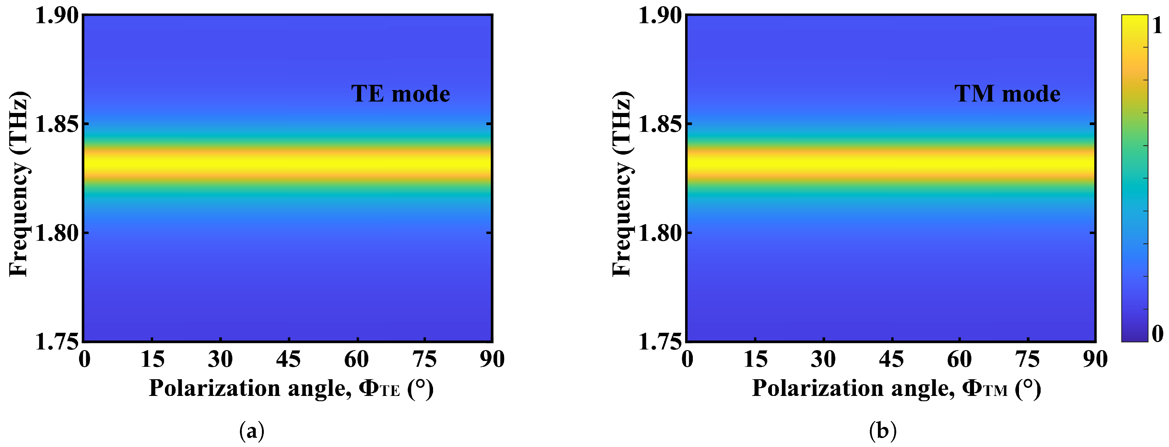
No magnetic bias is applied ( B = 0 ) in this section. Under these conditions the absorber is insensitive to the in-plane polarization angle for both TE and TM at normal incidence. To verify that the absorber retains its performance for any in-plane orientation of the incident field, we fixed the incidence at θ i = 0 and rotated the polarization angles Φ TE and Φ TM from 0 to 90 for TE and TM illumination, respectively. Figure 5a,b display the resulting absorbance spectra. Throughout the entire sweep, both the resonance frequency and the absorbance magnitude remain essentially unchanged—evidence that the device is insensitive to the orientation of the incident electric field. This behavior stems from the high rotational symmetry of the unit cell, which renders its electromagnetic response identical for any polarization direction in the xy plane. Accordingly, the absorber can be regarded as polarization-insensitive for both TE and TM modes under normal incidence.

3.5. Influence of Geometrical Parameters

To assess fabrication tolerances and provide design guidelines, we numerically varied one geometrical parameter at a time while keeping all others fixed and monitored both the absorbance lineshape and the peak resonance frequency f 0 (Figure 6). All simulations were carried out at T = 295 K under TE-polarized normal incidence.
(i)
Substrate thickness h
Figure 6a shows that when the InSb substrate is thinner than the skin depth in the 1.7–1.9 THz band ( δ skin 20 μ m ), a small fraction of the THz power leaks through and the peak absorbance drops to 85 % (case h = 10 μ m ). Once h exceeds the skin depth, both the peak absorbance and the resonance frequency saturate [Figure 6d]. Beyond h 20 μ m , the substrate behaves as an optically thick backing, so further increases in thickness do not influence the EM response.
(ii)
Pillar height t
Varying the pillar height between 95 and 110 µm [Figure 6b] reveals an optimal value near t opt = 100 μ m where the impedance is most closely matched to free space and the absorbance reaches unity. For t < t opt , the pillar is under-coupled and the peak absorbance falls sharply; for t > t opt , the absorbance also decreases and the resonance linewidth broadens, while the center frequency continues to red-shift [Figure 6e]. This behavior can be interpreted with a lumped LC model [32] in which the pillar height primarily tunes the equivalent inductance L, so that f 0 1 / L C decreases as t increases.
(iii)
Pillar radius R
Finally, sweeping the radius from 20 to 35 µm produces the strongest geometrical tuning [Figure 6c,f]. A larger R increases the capacitive overlap between the displacement currents and the surrounding field, thereby increasing the equivalent capacitance C and driving a pronounced red-shift. The peak absorbance remains above 90 % across the entire radius range, even though the center frequency moves by more than 140 GHz. Thus, moderate lithographic deviations in R affect the spectral position of the resonance rather than its strength and can later be compensated by magnetic or thermal tuning if precise frequency registration is required.
  • Design insight. Once the substrate is thicker than the THz skin depth, the absorber’s response is governed primarily by the aspect ratio of the InSb pillar. Varying the height t changes the inductive path length and provides a fine tuning knob: a ± 5 μ m deviation shifts the resonance by only a few GHz. However, moving away from the optimal height ( t opt 100 μ m ) also degrades the impedance match, causing the peak absorbance to drop from 100% to 70 % and broadening the linewidth.
Adjusting the radius R produces a coarse tuning effect. Because a larger R increases the effective capacitance of the pillar, it red-shifts the resonance by tens of GHz. Conversely, reducing R blue-shifts the response. Although the peak absorbance stays above 90 % across the tested radius range, the center frequency moves by more than 160 GHz, so R must be controlled carefully when a specific design frequency is required.

4. Tunability and Sensitivity

4.1. Thermal Tunability

The InSb resonator’s carrier density—and hence its plasma frequency—varies appreciably with temperature. To quantify the resulting spectral shift, we simulated the absorber at five ambient temperatures between 295 and 315 K under normal-incidence TE illumination. The absorbance curves in Figure 7a reveal a clear blue-shift of the resonance as T rises, while the peak magnitude remains above 95%.
The resonance frequency f res was extracted from each spectrum and plotted against temperature in Figure 7b. A least-squares fit yields a linear relation:
f res ( T ) = f 0 + S T ( T 295 K ) ,
where f 0 = 1.8317 THz and the thermal sensitivity is [33]
S T = Δ f res Δ T 2.8 GHz · K 1 .
The high coefficient of determination ( R 2 = 0.993 ) indicates that the frequency shift scales almost perfectly linearly with temperature within the investigated range.
Such a sensitivity, combined with the absorber’s narrow linewidth ( FWHM = 25.3 GHz at 295 K), translates to a figure of merit [34] FOM = S / FWHM 0.111 K 1 , demonstrating the device’s potential for compact THz thermometry or active thermal tuning in reconfigurable metasurfaces.
Concurrently, the 90% absorptance window ( Δ f A 0.9 ) reported in Figure 7a and Table 1 contracts smoothly from 8.3 GHz at 295 K to 3.3 GHz at 315 K. For comparison, we express selectivity using an illustrative standards-agnostic sub-channel grid (1.0 GHz center-to-center) to count how many contiguous channels fall within the 90% absorptance window. Even under the more conservative 1 GHz spacing, the metasurface, therefore, suppresses the following:
Δ f A 0.9 1 GHz = { 8.3 , 7.0 , 5.0 , 4.0 , 3.3 } 8 3 consecutive channels ( 295 315 K ) .
At room temperature (295 K), the metasurface can, thus, absorb eight consecutive 1 GHz-spaced channels without leaving spectral gaps; even at the highest investigated temperature (315 K), it still removes three full channels. This adaptability makes the metasurface a promising passive front-end for reconfigurable THz links, where contiguous sub-GHz selectivity is required.

4.2. Magnetic Tunability

Besides thermal control, the proposed absorber can be dynamically reconfigured by a static magnetic bias, thanks to the gyrotropic response of InSb. To quantify this effect, we simulated the structure at T = 295 K under normal-incidence TE illumination while sweeping the bias field B     x ^ from 0.1 to 0.4 T in 0.1 T steps. The corresponding absorbance spectra are displayed in Figure 8a. A clear red-shift of the resonance is observed as the field strength increases, whereas the peak absorbance remains close to unity.
The resonance frequency f res extracted from each curve is plotted against B in Figure 8b. A linear least-squares fit yields
f res ( B ) = f 0 + S B T E ( B 0.1 T ) ,
where f 0 = 1.83 THz and the magnetic sensitivity [13] is
S B T E = Δ f res Δ B 132.7 GHz · T 1 .
The negative slope confirms that the resonance frequency decreases monotonically with increasing bias, consistent with the increase in the transverse permittivity components of magnetized InSb, which reduces the phase velocity of the mode and consequently shifts the resonance to lower frequencies. The fit exhibits a high coefficient of determination ( R 2 = 0.980 ), confirming the nearly perfect linear dependence of the resonant frequency on the applied bias field.
Combining the magnetic sensitivity with the resonance linewidth ( FWHM = 26.3 GHz at B = 0.1 T) yields a figure of merit FOM = | S B T E | / FWHM 5.046 T 1 , indicating that the absorber can serve as an active component in magnetically tunable metasurfaces.
Under magnetic tuning, the 90% absorptance bandwidth ( Δ f A 0.9 ) reported in Figure 8a and Table 2 widens from 8.5 GHz at B = 0.1 T to 14.8 GHz at B = 0.4 T. With a conservative 1.0 GHz center-to-center grid (standards-agnostic), the metasurface thus eliminates the following:
Δ f A 0.9 1 GHz = { 8.5 , 10.0 , 11.8 , 14.8 } 8 14 consecutive channels ( 0.1 0.4   T ) .
A modest adjustment of the magnetic field allows the metasurface to broaden its stop-band from eight to fourteen consecutive channels, without introducing spectral gaps. This tunability highlights its use as a reconfigurable, channel-selective THz filter.
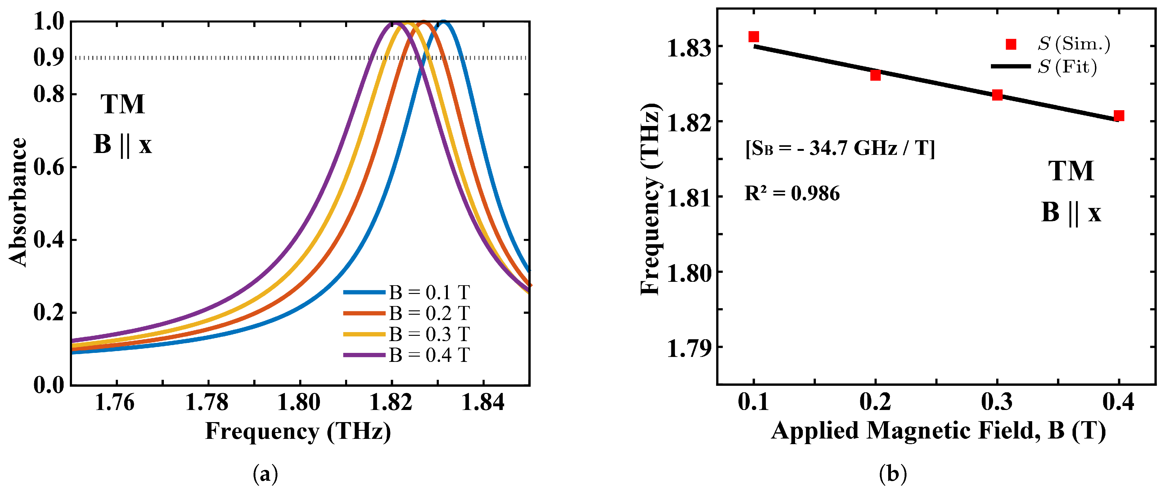
For TM illumination with E     x ^     B , the tuning is weaker because ε x x is magnetically invariant in Equation (5). The extracted slope is S B TM 34.7 GHz · T 1 with R 2 0.986 , while the peak absorbance remains 0.99 across B = [ 0.1 0.4 ] T as shown in Figure 9a,b. The contrast between S B T E and S B T M confirms that magnetic bias introduces polarization-dependent frequency shifts, in agreement with the magneto-Drude tensor in Equations (5)–(7).

5. Discussion

The preceding sections detail the electromagnetic response of an all-dielectric InSb cylindrical pillar metasurface that operates as a single-band, high-Q terahertz (THz) absorber with two independent tuning mechanisms. Here, we interpret these findings in light of earlier InSb absorbers, discuss the broader technological implications, and outline promising research avenues.
Table 3 benchmarks our InSb cylindrical pillar against representative single-band InSb absorbers in the literature. Two salient advantages stand out.

5.1. Spectral Selectivity

Our design attains a loaded quality factor of Q = 72.3 , surpassing the best purely dielectric metasurface reported by [35] ( Q = 53.2 ) and more than doubling the Q of the thermally tunable star-shaped absorber proposed by [12] ( Q = 26.9 ). The marked improvement stems from critical coupling between electric- and magnetic-dipole resonances co-supported by the solid InSb pillar. In contrast to split-ring or hybrid metal–dielectric structures, the low-loss semiconductor host suppresses Ohmic damping, while the cylindrical symmetry minimizes radiative leakage for both TE and TM polarizations. Together, these factors concentrate the electromagnetic energy and sharpen the absorption line, a prerequisite for narrowband THz filtering.

5.2. Dual Linear Tunability

Most prior InSb absorbers exploit either temperature control [12,35,37] or static magnetic bias [36]. By integrating both stimuli into a single, metal-free platform, our metasurface enables bidirectional control of its spectral position. The resonance blue-shifts at S T = 2.8 GHz · K 1 under heating and red-shifts at S B T E = 132.7 GHz · T 1 and S B T M = 34.7 GHz · T 1 under magnetic bias. Although these coefficients are lower than the record sensitivities reported for strictly monostimulus devices (9.6 GHz K−1 [12] and 300 GHz T−1 [36]), they are achieved with a simpler all-dielectric geometry that avoids metal layers and parasitics, while providing a linear tuning range across accessible temperature and magnetic field spans for THz spectral allocation.

6. Conclusions

We have designed and numerically validated an all-dielectric InSb metasurface that functions as a high-Q ( Q = 72.3 ), single-band perfect absorber at 1.83 THz. Critical coupling between orthogonal dipolar resonances yields near-unity absorbance. Leveraging the temperature-dependent carrier density and the magneto-optic response of InSb, the resonance can be tuned linearly at S T = 2.8 GHz · K 1 , S B T E = 132.7 GHz · T 1 and S B T M = 34.7 GHz · T 1 without compromising absorption strength under normal incidence.
Beyond frequency tuning, the metasurface demonstrates channel-level control in the 90% absorptance bandwidth ( Δ f A 0.9 ). Under temperature modulation from 295 K to 315 K, Δ f A 0.9 contracts from 8.3 GHz to 3.3 GHz, enabling suppression of 3–8 adjacent 1 GHz-spaced channels. Under magnetic-field bias from 0.1 T to 0.4 T, the bandwidth expands from 8.5 GHz to 14.8 GHz, corresponding to 8–14 consecutive channels. In both cases, the metasurface maintains gapless coverage, underscoring its potential as a reconfigurable, channel-selective filter.
The combination of sharp spectral selectivity, dual-mode tunability, and a simple, metal-free geometry positions the proposed metasurface as a promising component for reconfigurable THz devices, particularly in dense beyond-5G/6G terahertz scenarios and other THz links that demand contiguous sub-GHz spectral selectivity.

Author Contributions

Conceptualization, R.C.-B. and M.C.-A.; methodology, R.C.-B. and M.C.-A.; software, R.C.-B.; validation, J.L.-C. and M.C.-A.; formal analysis, R.C.-B., J.L.-C. and M.C.-A.; investigation, R.C.-B.; resources, M.C.-A.; data curation, R.C.-B.; writing—original draft preparation, R.C.-B.; writing—review and editing, M.C.-A. and J.L.-C.; visualization, R.C.-B.; supervision, J.L.-C. and M.C.-A.; project administration, M.C.-A. All authors have read and agreed to the published version of the manuscript.

Funding

This research received no external funding.

Data Availability Statement

The data presented in this study are openly available in Github at https://github.com/RafaelCharca/highQ-thz-insb-metasurface.git, accessed on 7 September 2025.

Acknowledgments

We would like to express our gratitude to the Electronics Circuits and Systems Research Group gECS-HF at the Universidad Nacional Tecnológica de Lima Sur for providing access to high-performance computing facilities and licensed simulation software that made this work possible.

Conflicts of Interest

The author declares no conflicts of interest.

References

  1. 3rd Generation Partnership Project. 5G NR; Physical Channels and Modulation (Release 17). 3GPP TS 38.211. 2022. Available online: https://www.etsi.org/deliver/etsi_ts/138200_138299/138211/17.01.00_60/ts_138211v170100p.pdf (accessed on 5 July 2025).
  2. Rappaport, T.S.; Xing, Y.; Kanhere, O.; Ju, S.; Madanayake, A.; Mandal, S.; Alkhateeb, A.; Trichopoulos, G.C. Wireless communications and applications above 100 GHz: Opportunities and challenges for 6G and beyond. IEEE Access 2019, 7, 78729–78757. [Google Scholar] [CrossRef]
  3. You, X.; Wang, C.-X.; Huang, J.; Gao, X.; Zhang, Z.; Wang, M.; Huang, Y.; Zhang, C.; Jiang, Y.; Wang, J.; et al. Towards 6G wireless communication networks: Vision, enabling technologies, and new paradigm shifts. Sci. China Inf. Sci. 2021, 64, 110301. [Google Scholar] [CrossRef]
  4. Tataria, H.; Shafi, M.; Molisch, A.F.; Dohler, M.; Sjöland, H.; Tufvesson, F. 6G wireless systems: Vision, requirements, challenges, insights, and opportunities. Proc. IEEE 2021, 109, 1166–1199. [Google Scholar] [CrossRef]
  5. Landy, N.I.; Sajuyigbe, S.; Mock, J.J.; Smith, D.R.; Padilla, W.J. Perfect metamaterial absorber. Phys. Rev. Lett. 2008, 100, 207402. [Google Scholar] [CrossRef]
  6. Liu, X.; Starr, T.; Starr, A.F.; Padilla, W.J. Infrared spatial and frequency selective metamaterial with near-unity absorbance. Phys. Rev. Lett. 2010, 104, 207403. [Google Scholar] [CrossRef]
  7. Wang, P.; He, F.; Liu, J.; Shu, F.; Fang, B.; Lang, T.; Jing, X.; Hong, Z. Ultra-high-Q resonances in terahertz all-silicon metasurfaces based on bound states in the continuum. Photonics Res. 2022, 10, 2743–2750. [Google Scholar] [CrossRef]
  8. Ye, L.; Chen, X.; Cai, G.; Zhu, J.; Liu, N.; Liu, Q.H. Electrically tunable broadband terahertz absorption with hybrid-patterned graphene metasurfaces. Nanomaterials 2018, 8, 562. [Google Scholar] [CrossRef]
  9. Charca-Benavente, R.; Kumar, R.; Rubio-Noriega, R.; Clemente-Arenas, M. Thermally tunable bi-functional metasurface based on InSb for terahertz applications. Materials 2025, 18, 2847. [Google Scholar] [CrossRef] [PubMed]
  10. Carvalho, W.O.F.; Moncada-Villa, E.; Mejía-Salazar, J.R.; Spadoti, D.H. Dynamic terahertz beamforming based on magnetically switchable hyperbolic materials. J. Phys. D Appl. Phys. 2024, 57, 175001. [Google Scholar] [CrossRef]
  11. Chen, F.; Cheng, Y.; Luo, H. Temperature tunable narrow-band terahertz metasurface absorber based on InSb micro-cylinder arrays for enhanced sensing application. IEEE Access 2020, 8, 82981–82988. [Google Scholar] [CrossRef]
  12. Luo, H.; Cheng, Y. Thermally tunable terahertz metasurface absorber based on all dielectric indium antimonide resonator structure. Opt. Mater. 2020, 102, 109801. [Google Scholar] [CrossRef]
  13. Clemente-Arenas, M.; Rubio-Noriega, R.E.; Urbina, J.V.; Lakhtakia, A. Non-metallic magnetostatically tunable metasurface absorber for terahertz waves. J. Opt. Soc. Am. B 2024, 41, 691–697. [Google Scholar] [CrossRef]
  14. Liu, M.; Wei, R.; Taplin, J.; Zhang, W. Terahertz metasurfaces exploiting the phase transition of vanadium dioxide. Materials 2023, 16, 7106. [Google Scholar] [CrossRef]
  15. Wen, C.; Feng, L.; Li, Z.; Bai, J.; Wang, S.; Gao, X.; Wang, J.; Yao, W. A review of the preparation, properties and applications of VO2 thin films with the reversible phase transition. Front. Mater. 2024, 11, 1341518. [Google Scholar] [CrossRef]
  16. Squires, A.D.; Gao, X.; Du, J.; Han, Z.; Seo, D.H.; Cooper, J.S.; Murdock, A.T.; Lam, S.K.H.; Zhang, T.; van der Laan, T. Electrically tuneable terahertz metasurface enabled by a graphene/gold bilayer structure. Commun. Mater. 2022, 3, 56. [Google Scholar] [CrossRef]
  17. Yang, J.; Zhu, Z.; Zhang, J.; Guo, C.; Xu, W.; Liu, K.; Yuan, X.; Qin, S. Broadband terahertz absorber based on multi-band continuous plasmon resonances in geometrically gradient dielectric-loaded graphene plasmon structure. Sci. Rep. 2018, 8, 3239. [Google Scholar] [CrossRef]
  18. Cheng, Y.; Cao, W.; He, X. Hybrid plasmonic waveguides with tunable ENZ phenomenon supported by 3D Dirac semimetals. Laser Photonics Rev. 2024, 18, 2400167. [Google Scholar] [CrossRef]
  19. Wang, G.; Cao, W.; He, X. 3D Dirac semimetal elliptical fiber supported THz tunable hybrid plasmonic waveguides. IEEE J. Sel. Top. Quantum Electron. 2023, 29, 8400207. [Google Scholar] [CrossRef]
  20. Wu, M.; Wu, L.; Tao, J. Research progress on two-photon 3D printed metasurface optical devices. Study Opt. Commun. 2023, 49, 11–31. [Google Scholar]
  21. Li, W.; Kuang, D.; Fan, F.; Chang, S.; Lin, L. Subwavelength B-shaped metallic hole array terahertz filter with InSb bar as thermally tunable structure. Appl. Opt. 2012, 51, 7098–7102. [Google Scholar] [CrossRef]
  22. Liu, H.; Ren, G.; Gao, Y.; Lian, Y.; Qi, Y.; Jian, S. Tunable subwavelength terahertz plasmon-induced transparency in the InSb slot waveguide side-coupled with two stub resonators. Appl. Opt. 2015, 54, 3918–3924. [Google Scholar] [CrossRef]
  23. Moridsadat, M.; Golmohammadi, S.; Baghban, H. Tunable multiband plasmonic response of indium antimonide touching microrings in the terahertz range. Appl. Opt. 2018, 57, 4368–4375. [Google Scholar] [CrossRef] [PubMed]
  24. Oszwałldowski, M.; Zimpel, M. Temperature dependence of intrinsic carrier concentration and density of states effective mass of heavy holes in InSb. J. Phys. Chem. Solids 1988, 49, 1179–1185. [Google Scholar] [CrossRef]
  25. Xia, L.; Zhang, X.; Wang, D.; Zhang, W.; Han, J. Terahertz surface magnetoplasmons modulation with magnetized InSb hole array sheet. Opt. Commun. 2019, 446, 84–87. [Google Scholar] [CrossRef]
  26. Han, J.; Lakhtakia, A.; Tian, Z.; Lu, X.; Zhang, W. Magnetic and magnetothermal tunabilities of subwavelength-hole arrays in a semiconductor sheet. Opt. Lett. 2009, 34, 1465–1467. [Google Scholar] [CrossRef]
  27. Islam, M.S.; Sultana, J.; Biabanifard, M.; Vafapour, Z.; Nine, M.J.; Dinovitser, A.; Cordeiro, C.M.B.; Ng, B.W.-H.; Abbott, D. Tunable localized surface plasmon graphene metasurface for multiband superabsorption and terahertz sensing. Carbon 2020, 158, 559–567. [Google Scholar] [CrossRef]
  28. Zhou, Q.; Ma, W.; Wu, T.; Li, Y.; Qiu, Q.; Duan, J.; Li, J.; Jiang, L.; Zhou, W.; Gao, Y.; et al. Metasurface terahertz perfect absorber with strong multi-frequency selectivity. ACS Omega 2022, 7, 36712–36727. [Google Scholar] [CrossRef]
  29. Yue, L.; Wang, Y.; Cui, Z.; Zhang, X.; Zhu, Y.; Zhang, X.; Chen, S.; Wang, X.; Zhang, K. Multi-band terahertz resonant absorption based on an all-dielectric grating metasurface for chlorpyrifos sensing. Opt. Express 2021, 29, 13563–13575. [Google Scholar] [CrossRef]
  30. Zhou, M.; Liu, D.; Belling, S.W.; Cheng, H.; Kats, M.A.; Fan, S.; Povinelli, M.L.; Yu, Z. Inverse design of metasurfaces based on coupled-mode theory and adjoint optimization. ACS Photonics 2021, 8, 2265–2273. [Google Scholar] [CrossRef]
  31. Liu, Y.; Huang, R.; Ouyang, Z. Terahertz absorber with dynamically switchable dual-broadband based on a hybrid metamaterial with vanadium dioxide and graphene. Opt. Express 2021, 29, 20839–20850. [Google Scholar] [CrossRef]
  32. Pozar, D.M. Microstrip antennas. Proc. IEEE 2002, 80, 79–91. [Google Scholar] [CrossRef]
  33. Wang, Y.; Qiu, Y.; Zhang, Y.; Lang, T.; Zhu, F. High-sensitivity temperature sensor based on the perfect metamaterial absorber in the terahertz band. Photonics 2023, 10, 92. [Google Scholar] [CrossRef]
  34. Chau, Y.-F.C.; Chao, C.-T.C.; Huang, H.J.; Anwar, U.; Lim, C.M.; Voo, N.Y.; Mahadi, A.H.; Kumara, N.T.R.N.; Chiang, H.-P. Plasmonic perfect absorber based on metal nanorod arrays connected with veins. Results Phys. 2019, 15, 102567. [Google Scholar] [CrossRef]
  35. Cheng, Y.; Li, Z.; Cheng, Z. Terahertz perfect absorber based on InSb metasurface for both temperature and refractive index sensing. Opt. Mater. 2021, 117, 111129. [Google Scholar] [CrossRef]
  36. Sharma, G.; Lakhtakia, A.; Bhattacharyya, S.; Jain, P.K. Magnetically tunable metasurface comprising InAs and InSb pixels for absorbing terahertz radiation. Appl. Opt. 2020, 59, 9673–9680. [Google Scholar] [CrossRef]
  37. Binda, P.; Singh, R.K.; Mitharwal, R. A highly sensitive terahertz temperature sensor based on polarization insensitive perfect metamaterial absorber with tunable characteristics. Opt. Mater. 2024, 148, 114940. [Google Scholar] [CrossRef]
Figure 1. (a) Three-dimensional perspective of a single unit cell under normal incidence ( θ i = 0 ) with a static magnetic field B     x ^ . (b) Top-view schematic of the same unit cell. The angles Φ TE and Φ TM denote the orientation of the incident electric field for TE and TM polarizations, respectively, measured relative to the bias direction.
Telecom 06 00070 g001
Figure 2. Frequency-domain response of the single-band perfect absorber illuminated by a TE wave at normal incidence ( θ i = 0 ) and room temperature ( T = 295 K). (a) Numerically obtained reflectance R sim , transmittance T sim , and absorbance A sim , together with the absorbance predicted by coupled-mode theory A CMT . (b) Retrieved effective impedance, displaying its real and imaginary parts, Re { Z eff } and Im { Z eff } , respectively.
Telecom 06 00070 g002
Figure 3. Spatial field maps for the proposed perfect absorber excited by a TE-polarized plane wave at normal incidence ( θ i = 0 ) and T = 295 K. Results are shown at the resonance frequency f 0 = 1.8317 THz: (a) electric-field distribution on the central yz cross-section of the unit cell; (b) magnetic-field distribution on the central xz cross-section of the same unit cell.
Telecom 06 00070 g003
Figure 4. Spatial distributions at the resonance frequency f 0 = 1.8317 THz for the proposed perfect absorber excited by a TE-polarized plane wave at normal incidence ( θ i = 0 ) and T = 295 K : (a) power flow (Poynting vector) and (b) power-loss density within a single unit cell.
Telecom 06 00070 g004
Figure 5. Simulated absorbance spectra of the proposed single-band perfect absorber at T = 295 K and normal incidence ( θ i = 0 ). (a) TE polarization for Φ TE = 0 90 ; (b) TM polarization for Φ TM = 0 90 .
Telecom 06 00070 g005
Figure 6. Simulated absorbance spectra of the proposed single-band perfect absorber under TE-polarized illumination at normal incidence ( θ = 0 ) and ambient temperature ( T = 295 K), for varying geometric parameters: (a) thickness h of the InSb substrate, (b) height t, and (c) radio length R of the InSb cylindrical pillar structure. Subfigures (df) show the corresponding variation in peak absorption frequencies ( f 0 ) as functions of the respective parameters h, t, and R.
Telecom 06 00070 g006
Figure 7. Temperature tunability of the proposed single-band absorber under normal-incidence TE illumination. (a) Simulated absorbance spectra for five temperatures ( T = 295 , 300, 305, 310, and 315 K), showing a blue-shift of the resonance as T increases. (b) Extracted resonance frequency (red squares) versus temperature and the corresponding linear fit (black line), yielding a thermal sensitivity of S T 2.8 GHz · K 1 .
Telecom 06 00070 g007
Figure 8. Magnetic tuning behavior of the single-band absorber under normal-incidence TE illumination with a static bias B     x at T = 295 K. (a) Simulated absorbance spectra for four static magnetic-field strengths B = 0.1 , 0.2, 0.3, and 0.4 T, showing a progressive red-shift of the resonance as B increases. (b) Resonance frequency extracted from each spectrum (red squares) and linear fit (black line), yielding a magnetic sensitivity of S B TE 132.7 GHz · T 1 with R 2 = 0.980 .
Telecom 06 00070 g008
Figure 9. Magnetic tunability of the proposed single-band absorber under normal-incidence TM illumination with a static bias B     x at T = 295 K. (a) Simulated absorbance spectra for B = 0.1 , 0.2 , 0.3 , and 0.4 T , showing a slight red-shift of the resonance as B increases while the peak absorbance remains 0.99 . (b) Extracted resonance frequency f 0 versus B and the linear fit (black line), yielding a magnetic sensitivity of S B T M = 34.7 GHz · T 1 with R 2 = 0.986 .
Telecom 06 00070 g009
Table 1. Peak absorptance metrics of the metasurface versus temperature in the range 295–315 K.
T (K) A max f max A (GHz) Δ f A 0.9 (GHz)
2950.99918328.3
3000.99718497.0
3050.99218645.0
3100.98418754.0
3150.98318883.3
A max peak absorptance; f max A frequency of maximum absorption; Δ f A 0.9 90%-absorptance bandwidth.
Table 2. TE-polarized absorptance metrics vs. magnetic bias (0.1–0.4 T).
B (T) A max f max A (GHz) Δ f A 0.9 (GHz)
0.10.99918308.5
0.20.999182010.0
0.30.997180811.8
0.40.997179014.8
A max peak absorptance; f max A frequency of maximum absorption; Δ f A 0.9 90%-absorptance bandwidth.
Table 3. Performance comparison with representative single-band InSb-based THz absorbers from the literature.
ReferenceResonator/Tuning Method f 0 (THz)Peak A (%)Q S T (GHz/K) S B (GHz/T)Pol. Indep.
This workInSb cylindrical pillar/B and T tuning1.832≈10072.32.8132.7Yes
Luo & Cheng 2020 [12]InSb star-shaped/T tuning1.43099.926.99.6Yes
Cheng et al., 2021 [35]InSb micro-rod/T tuning1.75799.953.24.2Yes
Sharma et al., 2020 [36]Pixelated InAs/InSb/B tuning2–495–99300
Binda et al., 2024 [37]Curved InSb microstrip/T tuning1.84699.916.1Yes
B and T denote magnetic-field and temperature tuning, respectively. Q is computed as f 0 / Δ f 3 dB . Sensitivities S T and S B are defined as the absolute resonance shift per unit temperature or magnetic field. The first row corresponds to the results of this work.
Disclaimer/Publisher’s Note: The statements, opinions and data contained in all publications are solely those of the individual author(s) and contributor(s) and not of MDPI and/or the editor(s). MDPI and/or the editor(s) disclaim responsibility for any injury to people or property resulting from any ideas, methods, instructions or products referred to in the content.