Article

Development of Projection Optical Microscopy and Direct Observation of Various Nanoparticles

Health and Medical Research Institute, National Institute of Advanced Industrial Science and Technology (AIST), Central 6, Higashi, Tsukuba 305-8566, Japan
Optics 2025, 6(4), 50; https://doi.org/10.3390/opt6040050
Submission received: 25 August 2025 / Revised: 19 September 2025 / Accepted: 1 October 2025 / Published: 9 October 2025
(This article belongs to the Section Engineering Optics)

Abstract

The optical microscope is an indispensable observation instrument that has fundamentally contributed to progress in science and technology. Dark-field microscopy and scattered light imaging techniques enable high-contrast observation of nanoparticles in water. However, the scattered light is focused by the optical lenses, resulting in a blurred image of the nanoparticle structure. Here, we developed a projection optical microscope (PROM), which directly observes the scattered light from the nanoparticles without optical lenses. In this method, the sample is placed below the focus position of the microscope’s objective lens and the projected light is detected by an image sensor. This enables direct observation of the sample with a spatial resolution of approximately 20 nm. Using this method, changes in the aggregation state of nanoparticles in solution can be observed at a speed faster than the video frame rate. Moreover, the mechanism of such high-resolution observation may be related to the quantum properties of light, making it an interesting phenomenon from the perspective of optical engineering. We expect this method to be applicable to the observation and analysis of samples in materials science, biology and applied physics, and thus to contribute to a wide range of scientific, technological and industrial fields.

1. Introduction

Since its invention, the optical microscope has become one of the most important observation devices in modern science and technology [1,2,3,4]. Optical microscopes, in general, enable observation of microscopic samples by focusing light using lenses and other optical devices based on the diffraction properties of light in the form of waves [5,6,7]. The spatial resolution of such optical microscopes is limited to about half the wavelength resolution (200 nm) based on the diffraction theory formulated by Abbe [3,8]. Recently, the development of super-resolution fluorescence optical microscopy has made it possible to observe and analyse the location of fluorescently labelled proteins in cells with nano-level resolution [3,9,10,11,12]. Thus, improvements in the resolution and functionality of optical microscopy have been directly related to advances in science and technology.
However, in addition to diffraction, light is known to exhibit scattering [13]. For example, Rayleigh scattering occurs when light collides with and is absorbed and scattered by nitrogen and oxygen molecules in the atmosphere [13,14]. If Rayleigh scattering generated by such extremely small particles could be directly imaged, it should be possible to observe them with very high spatial resolution. To achieve this, a new optical system is needed that does not use lenses or other diffraction-based optical devices as used in conventional optical microscopes. Here, we report the development of a projection optical microscope (PROM) for direct observation of nanoparticles and nanostructures of 100 nm or less without the need for fluorescent labels and/or staining.
Light has particle properties in addition to wave properties. In 1905, Einstein’s light quantum hypothesis explained the photoelectric effect, in which electrons are emitted when light is shone on a metal surface, by assuming the particle nature of light as a photon [15]. Recent theoretical research has suggested that the classical interference phenomenon, a characteristic of light waves, arises from a special phenomenon known as entanglement, which occurs between the quantum bright and dark states of photons [16]. This theory suggests that the light interference phenomena can be interpreted as a quantum mechanism involving photons. Furthermore, recent theoretical research has also suggested that beam splitters may also be affected by quantum interference between the bright and dark states of photons [17]. Therefore, in the PROM observation method described here, it is possible that the interference is reduced due to the breakdown of entanglement between the bright and dark states of photons diffused through nanoscale structures, enabling high-resolution observation.

2. Materials and Methods

2.1. Raman Microscopy and PROM System

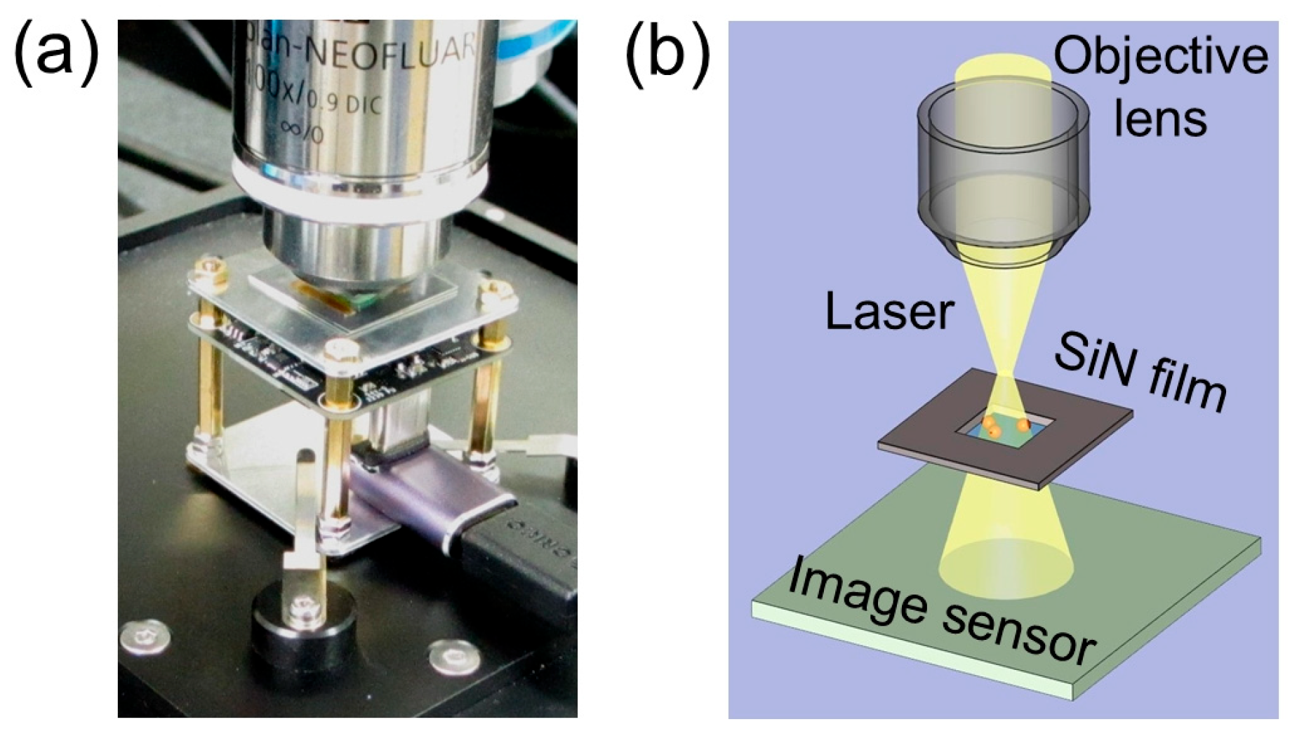
The samples on a silicon nitride (SiN) film (Silson Ltd., Southam, UK) were observed by a confocal laser Raman microscope (CLRM) (alpha300R, WITech, Ulm, Germany) using a 100× objective lens (Plan apo, Carl Zeiss, Oberkochen, Germany) and a 532 nm Nd-YAG laser. The CMOS image sensor (DFM37UX273-ML, The Imaging Source Co., Ltd., Bremen, Germany) was placed 5 mm below the focus position of the objective lens (Figure 1a,b). The video output of the CMOS image sensor was recorded by a PC (Let’s Note CF-FV4SRCCP, Panasonic Co., Tokyo, Japan) using image capture software (ICCapture ver. 2.5.1571, The Imaging Source Co., Ltd., Bremen, Germany) via a USB 3.1 cable. This image sensor is capable of imaging colour at 1440 × 1080 pixels with a pixel size of 3.45 μm (CMOS IMX273, Sony Co., Tokyo, Japan). Videos of the samples were captured at 1440 × 1080 pixels at a colour image capture rate of 60–100 fps. Video files recorded in Mpeg4 format were transferred to a desktop PC (Endeavor Pro 9200, Epson direct Co., Nagano, Japan). Image analysis was performed using MATLAB R2023a (Math Works Inc., Natick, MA, USA) and plotted using Origin 2023J (Origin-Lab Co., Northampton, MA, USA).
To obtain PROM video data, the sample was first aligned with the focal position of the CLRM and the focus position was then moved by 3 to 10 μm above the sample for observation using PROM. For the PROM observation of PS spheres, ZnO, and sunscreen, a 10 × 10 μm area was raster scanned (50 × 50 vertical and horizontal lines) for 4 min using the 2D map imaging mode of CLRM, during which video images were continuously captured by the image sensor. For the observation of milk using PROM, the sample was fixed and the same position was captured on video for 1 min.

2.2. Preparation of PS Spheres

The PS spheres of 1 μm or 500 nm diameter suspended in aqueous buffer (Micromer, micromod Partikeltechnologie GmbH, Rostock, Germany) were diluted three times with ultrapure water, vortexed for 10 s and sonicated for 1 min. A sample of the sphere suspension (5 μL) was placed on a 50 nm thick SiN film (0.5 × 0.5 mm window) supported by a Si frame (5 × 5 mm, 0.2 mm thick, Silson Ltd., Southam, UK) after hydrophilization for 15 s (PIB-10, Vacuum Device Inc., Mito, Japan). The liquid of the suspension was absorbed by a piece of filter paper from the droplet. The sample was dried for 5 min at room temperature (23 °C). The SiN film with the PS spheres was attached to an aluminium sample stage with a 3 mm hole in the centre (Figure 1a). For observation of the PS spheres by PROM, the focus position was set to 10 μm above the sphere sample, the laser light intensity was 0.1 mW, and video imaging was performed at 1440 × 1080 pixels at a speed of 60 frames per second (fps). When saving as an Mpeg4 file, the compression rate was set to 50MB/s.

2.3. ZnO Sample Preparation

ZnO particles of 20 nm diameter (260-01261, FUJIFILM Wako Pure Chemicals Co., Osaka, Japan) were suspended in pure water at a concentration of 10%/W and dispersed using an ultrasonic device for 2 min. 3 μL of this suspension was dropped onto the SiN film after hydrophilization. The excess liquid in the suspension was absorbed by filter paper and the sample was dried at room temperature (23 °C) for 5 min. The ZnO sample on the SiN film was attached to the centre of the cover glass with double-sided tape with the sample facing downwards and these were fixed to the sample stage.
For observation of the ZnO particles by PROM, the focus position was set to 3–10 μm above the sample, the laser light intensity was 0.1 mW, and the video imaging conditions were 1440 × 1080 pixels at a speed of 60 fps. When saving as an Mpeg4 file, the compression rate was set to 50 MB/s.

2.4. Sunscreen Sample Preparation

In the case of sunscreen containing TiO2 and ZnO nanoparticles (Sun play super cool, ROHTO Pharmaceutical Co., Ltd., Osaka, Japan), 2 µL of a sunscreen emulsion was dropped onto a tungsten-coated 50 nm thick SiN film (Silson Ltd., Southam, UK) that had been hydrophilized for 15 s. The SiN film with the sample was placed in a centrifuge holder and centrifuged at 2000 rpm for 1 min (MX300, Tommy Seiko Co., Tokyo, Japan) to thinly spread the sample on the SiN film.
For observation of the sunscreen sample by PROM, the focus position was set to 5 μm above the sample, the laser light intensity was 0.2 mW, and the video imaging conditions were 1440 × 1080 pixels at a speed of 60 fps. When saving as an Mpeg4 file, the compression rate was set to 50 MB/s.

2.5. Whole Milk Sample Preparation

The Si frame of a 50 nm thick SiN film was fixed to the cover glass with two strips of double-sided tape on both sides. Since the double-sided tape was 10 μm thick, there was a 10 μm gap between the SiN film and the cover glass. 2 μL of whole milk was dropped into the gap using an Eppendorf pipette (Eppendorf Co., Hamburg, Germany). The milk enters the gap between the cover glass and the SiN film due to surface tension. After that, the periphery of the SiN film chip was sealed with adhesive (RT30 ARALDITE, Huntsman Japan, Kobe, Japan) and kept at room temperature (23 °C) for 10 min. The milk suspension in its holder was fixed onto an aluminium sample stage with a 3 mm hole in the centre and was then observed using optical microscopy and PROM.
For observation of the milk sample by PROM, the focus position was set to 5 μm above the sample, the laser light intensity was 0.1 mW, and the video imaging conditions were 1440 × 1080 pixels at a speed of 100 fps. When saving as an Mpeg4 file, the compression rate was set to 50 MB/s.

2.6. Learning of Growing Neural Gas Network (GNG)

As the learning data for Growing Neural Gas Network (GNG) [18,19], we used an image obtained by extracting the high-frequency components of the PROM images and cutting out the central area of 400 × 400 pixels. The number of learning images for each sample was 14,350 for the PS spheres and the ZnO sample, 14,400 for the sunscreen sample, and 6000 for the milk sample. The number of GNG units was 100 units inside the PS sphere image and 50 units outside for the sphere samples, 20 units for the ZnO particles, 20 units for the sunscreen sample, and 10 units for the milk sample. The number of learning sessions was set to 200,000 iterations.

2.7. SEM and SE-ADM Observation of Samples

The ZnO sample on the SiN film with the Si frame was fixed on an aluminium stage with a conductive carbon tape and observed using a secondary electron image of the scanning electron microscope (SEM) (JSM7000F, JEOL, Tokyo, Japan). The ZnO sample was observed at an acceleration voltage of 4 kV and a current of 5–10 pA with a magnification of 20,000–40,000× and 1280 × 1024 pixel images were captured in 40 s.
For the scanning electron assisted dielectric microscopy (SE-ADM) observation [20,21] of the sunscreen sample, images of 1280 × 1020 pixels were captured over a period of 40 s at a magnification of 10,000–20,000× with an acceleration voltage of 10 kV and a current of 10 pA.

3. Results

3.1. Observation of Microspheres by Projection Optical Microscopy

In the PROM, a CLRM was used with an image sensor placed 5 mm below the focus position of the objective lens (Figure 1a,b). A sample was placed at the focus position of the CLRM for observation by light microscopy. Then, the focus position is moved 3 to 10 μm above the sample, which was irradiated using a 532 nm laser beam. The projected image of the sample was acquired by an image sensor at the bottom (Figure 1a,b). This projected image is magnified according to the distances of the sample from the focus position and the image sensor. In our system, the sample was 5 µm away from the focus position and 5 mm from the image sensor. Thus, the sample image was magnified approximately 1000 times and projected onto the image sensor. In this case, the size of one pixel of the sample image on the image sensor is 1/1000 of the actual pixel size.
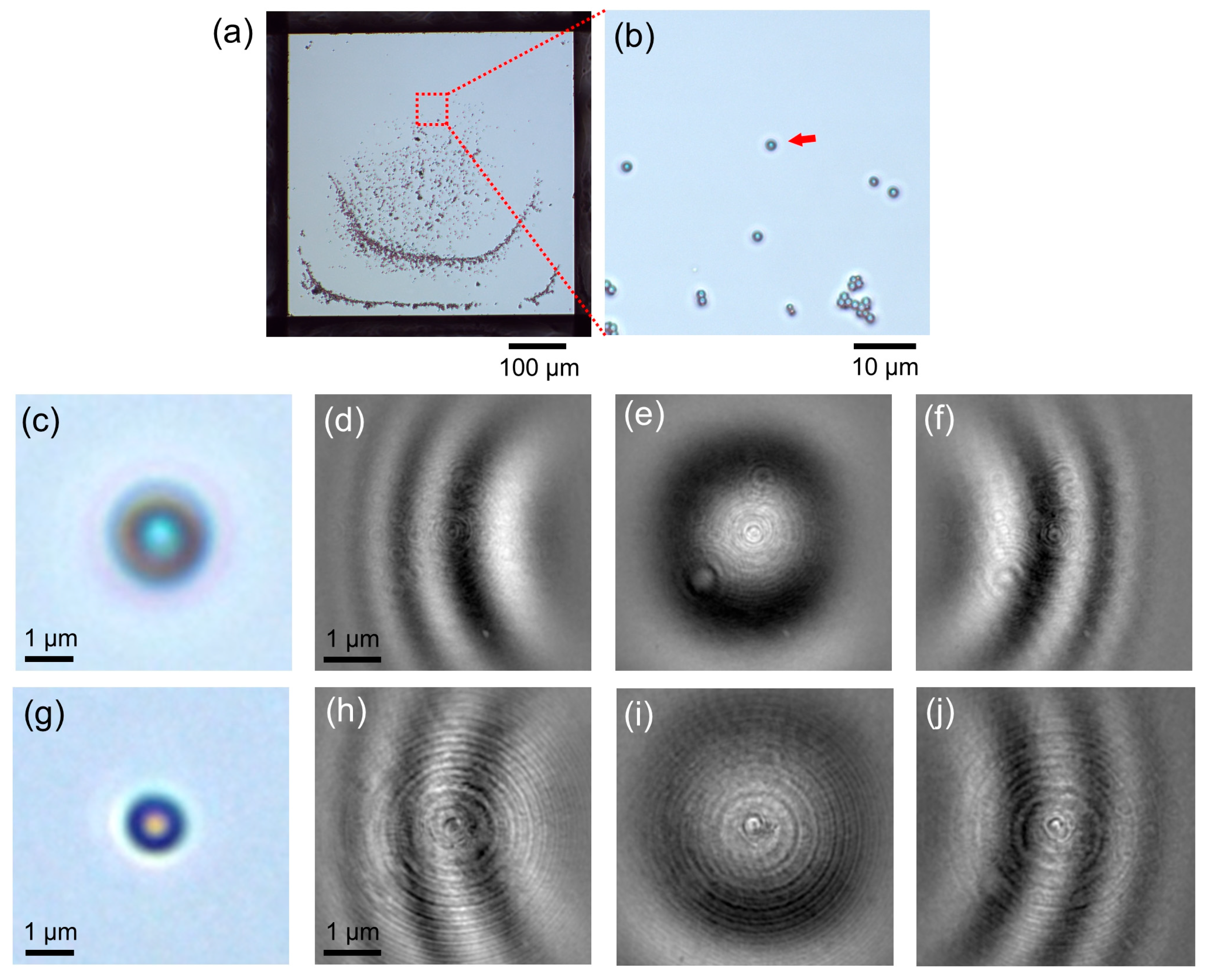
We first studied 1 µm polystyrene (PS) spheres dispersed on a 50 nm thick silicon nitride (SiN) film (Figure 2a–f). Initial observation by optical microscopy using CLRM showed the spheres to be well dispersed (Figure 2a–c). The focus position was then shifted to a position 10 μm above the sample and a 10 × 10 µm area centred on the spheres indicated by the arrow in Figure 2b was scanned in laser scanning mode. Images were continuously captured by the lower image sensor (Figure 2d–f, Supplementary Video S1). In the PROM image of the 1 µm diameter sphere, which is projected at a large magnification, arc-shaped stripes due to diffraction and interference were observed around the sphere (Figure 2d–f, Supplementary Video S1). In addition, interference fringes due to the cover glass directly above the image sensor and diffraction fringes were also observed due to small dust particles (Supplementary Video S1). This noise was observed in almost all areas in the image and was not affected by shifting the sample. Therefore, we removed the background noise components at the test location by subtracting the class-averaged image using GNG [18,19].
Similar patterns of diffraction and interference stripes were also observed around 0.5 μm polystyrene spheres (Figure 2g–j). These results indicate that both light diffraction and interference occurred in micrometre-sized samples. Thus, micrometre samples behave as expected in optical microscopy, whereby diffracted light from a sample is focused by a lens to magnify the image for observation and the spatial resolution is limited by the diffraction of light [4,8].

3.2. Background Subtraction of PROM Images

The PROM image acquired as video data was converted to a grey image by adding the RGB intensity values from the colour image. The high-frequency component image is calculated by subtracting each of these images and its Gaussian filter image with a σ value of 5 pixels. The 400 × 400 pixel area in the centre of the image was then cropped and used as training data. All the frames in the video were used for training. The number of frames used was 14,350 for the PS sphere and the ZnO sample, 14,400 for the sunscreen sample and 6000 for the milk sample.
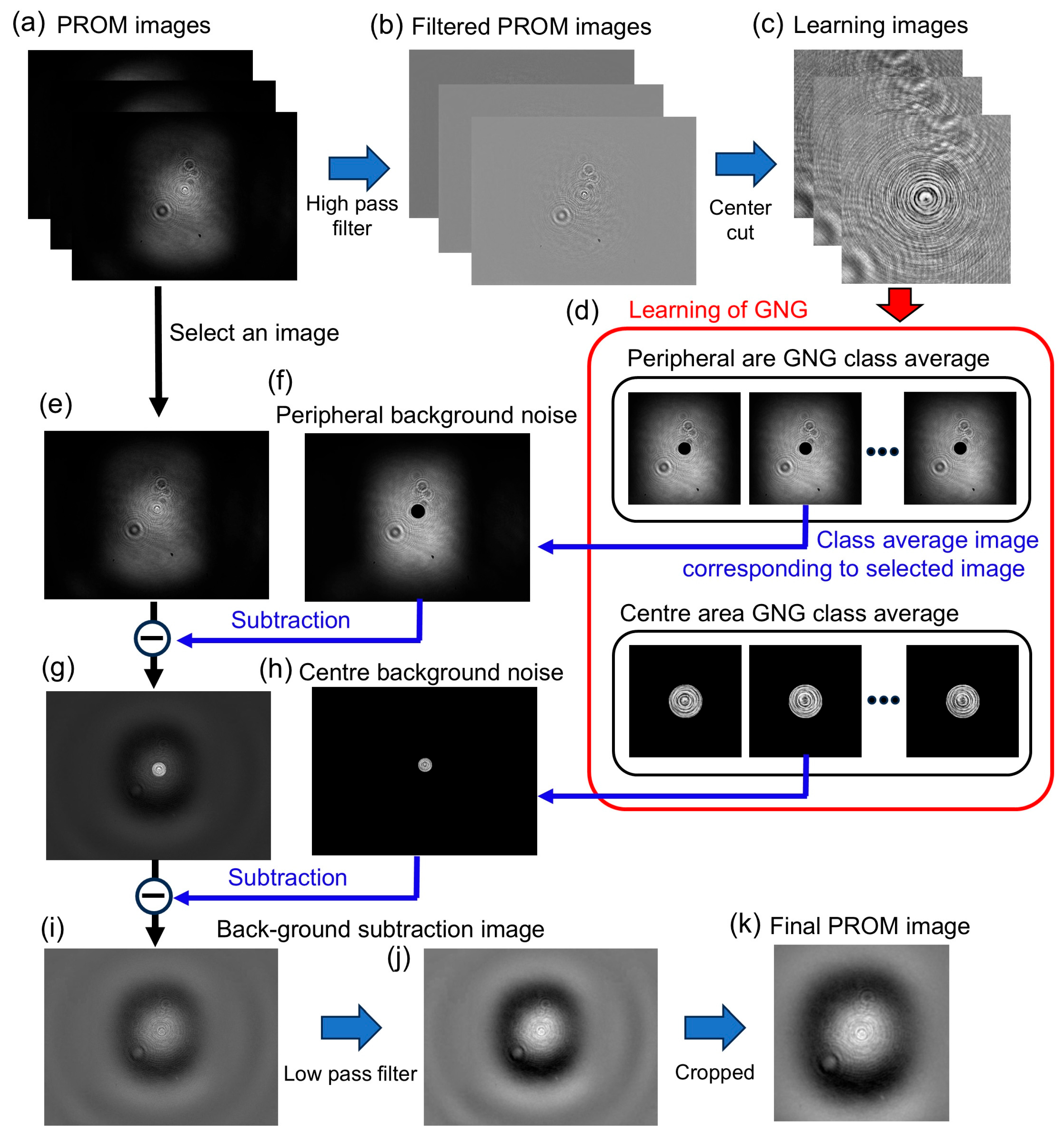
The PS sphere showed a strong diffraction pattern noise due to the image sensor cover. To remove this, the GNG [18,19] was trained on two separate sets of data, one in the middle of the image and the other at the periphery (Figure 3 and Figure 4). The images of the training data were divided into a central area of 150 pixels in diameter and an outer area of 150 pixels in diameter, each of which was trained by GNG (Figure 3). Background was subtracted twice from each PROM image using the corresponding GNG class-averaged image, once at the periphery and once at the centre. This was performed for all the PROM observation images (Figure 3).
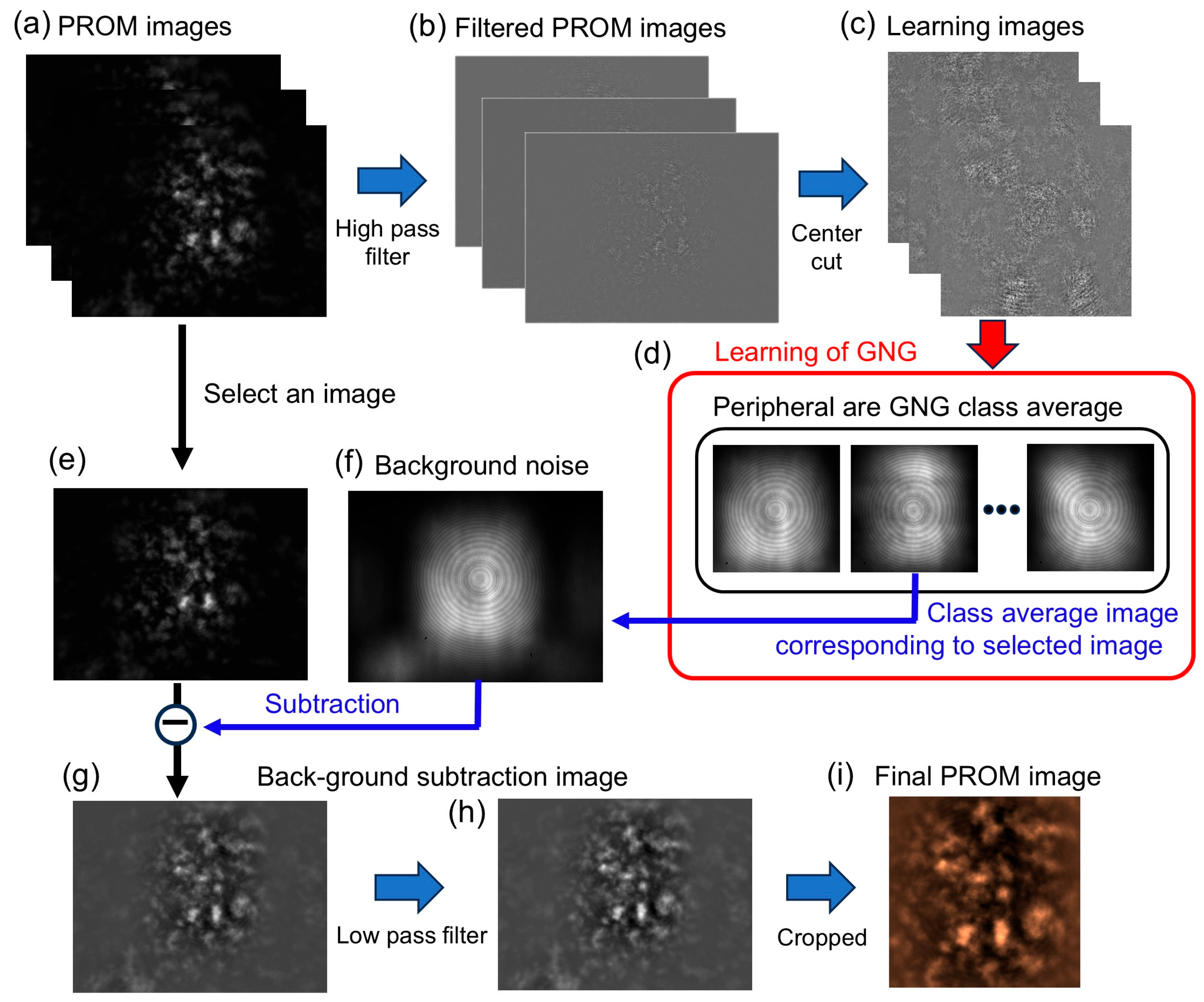
For the ZnO, sunscreen and milk samples, GNGs were trained using the entire 400 × 400 pixel image cropped from the centre due to the low background noise (Figure 4). One PROM image was then selected and the corresponding GNG class-averaged image subtracted.

3.3. Observation of ZnO Particles

Next, we used the same method to study samples at the nanometre scale. ZnO particles (20 nm diameter) were observed using our PROM system (Supplementary Video S2) and compared with SEM images (Figure 5). The ZnO sample was attached to the underside of the SiN film. Observation in CLRM optical microscope mode revealed an aggregate of fine particles and a narrow valley-like structure (Figure 5a–c). In the SEM image taken at the same location as in Figure 5d, ZnO particles were aggregated and both stacked and narrow valley structures were clearly observed. We enlarged the area of the red square-1 from Figure 5c and compared it with the PROM image at the same position (Figure 5e,f). In the optical microscope image, dark particle areas and light areas were observed as indistinct blurred patterns and no clear structure can be seen (Figure 5e). On the other hand, in the PROM image of the same area, the structures of particle aggregates and valleys could be observed very clearly (Figure 5f, Supplementary Video S2). In the SEM image at the same position, the aggregated parts of the particles appeared white while the valleys were dark (Figure 5g).
Figure 5h–j show the enlarged red square from Figure 5e–g. With an optical microscope, the entire image is extremely blurred and no clear structure could be identified (Figure 5h). On the other hand, in the PROM and SEM images, the aggregated and valley structures of ZnO were clearly observed (Figure 5i,j). In order to compare the PROM and SEM images in more detail, the areas indicated by the arrows in Figure 5i and j were further enlarged (Figure 5k). To match the contrast of the SEM image, that of the PROM images in Figure 5k was inverted and the colours were changed to produce white and dark blue pseudo-colours. In these enlarged images, characteristic elongated cylindrical valleys were observed and a structure similar to that seen in SEM could also be observed with PROM (Figure 5k). Furthermore, we enlarged the area of the red square-2 from Figure 5c,d and compared the images (Figure 5l–n). Although no clear structure was visible using the optical microscope (Figure 5l), PROM and SEM revealed almost the same structures (Figure 5m,n, red arrows). However, whereas SEM observes the surface structure of a sample, the PROM method observes light transmitted through the sample. Consequently, because the physical observation methods differ, the images obtained by the two techniques do not match perfectly. These results provide a qualitative comparison.
We measured spatial resolution using images of ZnO particle aggregates. Generally, in high-resolution observation methods such as electron microscopes, sharp-edge images are used to measure spatial resolution [22]. The brightness intensity of a linear plot of a sharp-edge image is normalised, and the resolution is defined as the width of the rising edge between 0.25 and 0.75 [22]. The resolution of the sharp edges of the valleys in the PROM image (Figure 5m, white arrow) was found to be approximately 16.6 nm (Figure 5o). This spatial resolution is much higher than the diffraction limit of conventional optical microscopy. Such a high spatial resolution by PROM is due to the fact that the PROM method acquires information only from Rayleigh scattering of nanoparticles, which does not cause diffraction of light, and thus the diffraction limit of light is of no relevance. However, this spatial resolution of 16.6 nm was measured from the sharp edge of ZnO particle aggregates observed in air. Therefore, this resolution is a value obtained under extremely good observation and specimen conditions. Samples containing highly concentrated nanoparticles in aqueous solution may further reduce resolution due to multiple scattering and the effects of water. Furthermore, thick samples that cause multiple scattering also result in reduced resolution and increased background noise.

3.4. Observation of Nanoparticles in a Sunscreen Sample

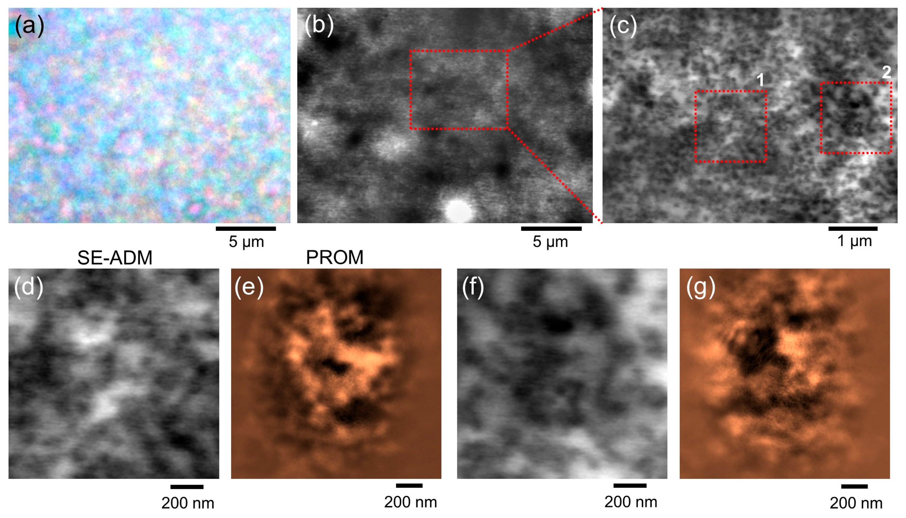
We next studied a commercial sunscreen consisting of TiO2 and ZnO nanoparticles dispersed in an emulsion (Figure 6, Supplementary Video S3). The optical microscope image of a thin layer of sunscreen applied to a tungsten-coated SiN film is blurred and appears like a polka dot pattern with no clearly visible nanoparticles (Figure 6a). We also examined the same sample using SE-ADM [20,21], which can resolve biological samples and organic materials in solution [21,23]. Figure 6b shows a low-magnification image of the sunscreen sample using SE-ADM. In the high-magnification image (Figure 6c), TiO2 and ZnO nanoparticles in the sunscreen were clearly discerned. In the enlarged image of the red square-1 in Figure 6c, a characteristic inverted triangular valley could be seen in the centre (Figure 6d). The PROM image at the same position indicated a similar inverted triangular valley (Figure 6e). The dispersion and structures of particles in the enlarged images of SE-ADM and PROM were almost identical in different areas (Figure 6f,g). SE-ADM irradiates a thin film with an electron beam, and the resulting potential change is observed by transmitting it through the sample [20,21]. Therefore, the observed image is a transmitted image, which is consistent with the PROM image.

3.5. Direct Observation of Whole Milk by PROM

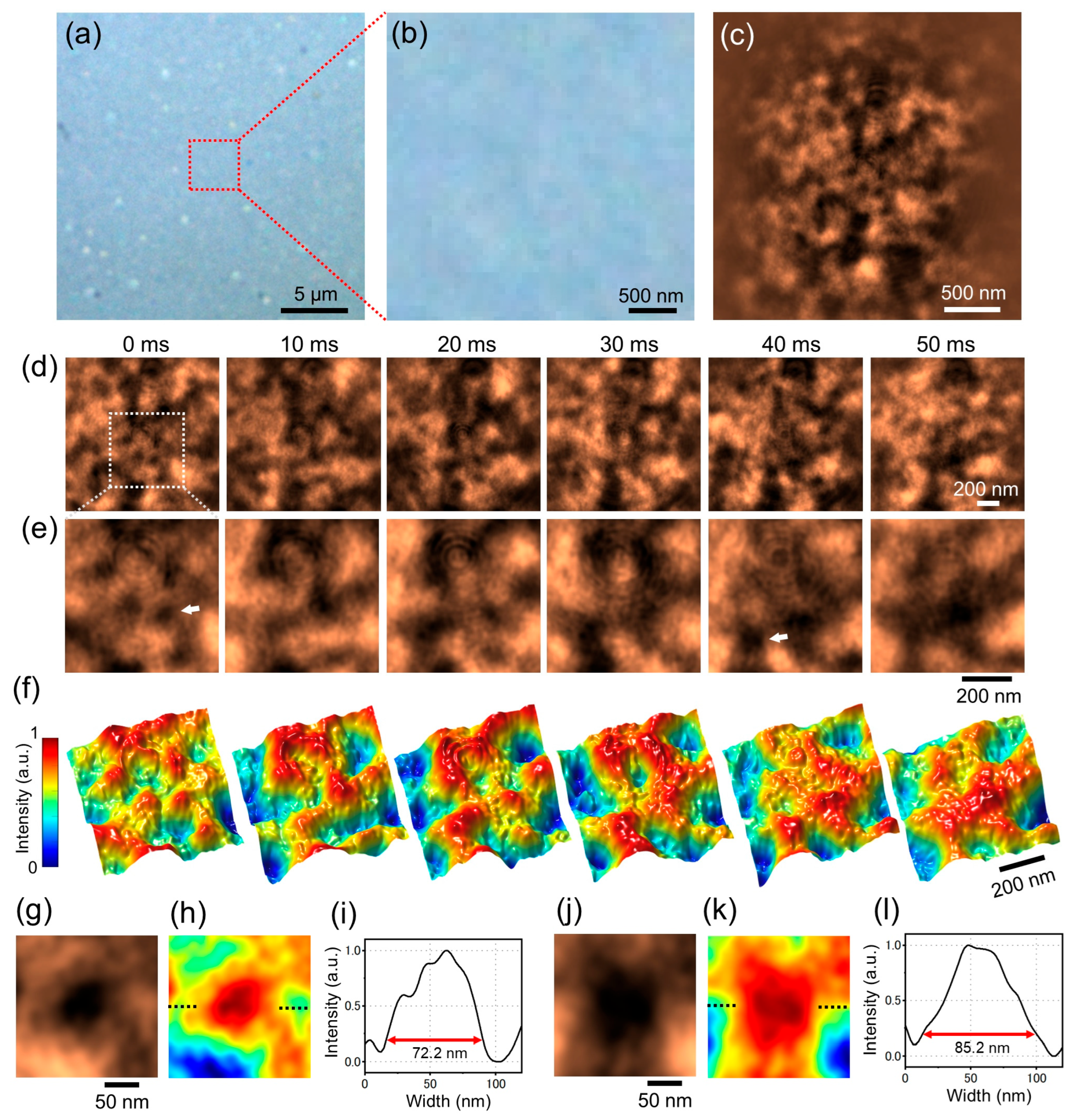
Finally, we examined milk using PROM (Figure 7). Whole milk was placed between a SiN film and a cover glass with a 10 μm spacer in between. The surrounding area was sealed with adhesive. In optical microscope images, the white milk fat could be observed, but nanoparticles such as casein micelles were not visible (Figure 7a,b). In PROM images, however, casein micelles and other nanoparticles could be clearly observed (Figure 7c). In this PROM experiment, the sample position was fixed and a video was made of the same location at a speed of 100 images per second. The dynamic changes in the nanoparticles, which repeatedly disperse and aggregate at high speed, were clearly observed (Supplementary Video S4). Figure 7d shows enlarged images of the centre of Figure 7c, six images being taken from 0 to 50 msec, in which dark nanoparticles are rapidly assembled and dispersed by Brownian motion. In the more highly enlarged image of the white square in Figure 7d and the pseudo three-dimensional map (Figure 7e,f), it is possible to see in more detail how the nanoparticle aggregate structure changes dynamically. Furthermore, we enlarged the area where a single casein micelle was located and measured its diameter, which confirmed it to be approximately 70–90 nm (Figure 7g–l). This is consistent with results using conventional methods [24,25,26]. Direct observation of nanoparticles undergoing rapid Brownian motion in solution is difficult, even with SEM, liquid SEM, or SE-ADM. Therefore, a direct comparison with conventional methods was not performed here.

4. Discussion

In this study, we have demonstrated the feasibility of directly observing nano-scale particles and structures by irradiating samples with diffused light and directly capturing the images with an image sensor (Figure 2 and Figure 5). In conventional optical microscopes, images are magnified and observed by focusing diffracted light from submicron or larger structures using lenses [5,6,7,8]. In such conventional microscopes, the spatial resolution is limited by light diffraction [3,8]. However, nanoparticles can also scatter light at the molecular level [13,14]. In Rayleigh scattering, light is scattered even by very small molecules in the atmosphere [13,14]. If such Rayleigh scattering information could be directly obtained, it would be possible to achieve molecular-level spatial resolution. This method is independent of diffraction, so light diffraction limits do not come into play.
We have developed a PROM in which the sample is placed below the focus position of the objective lens of a CLRM, and an image sensor is installed further below (Figure 1). With this method, interference fringes due to light diffraction and interference were indeed observed with particles larger than submicron (Figure 2d–f, Figure 8a). On the other hand, nanoparticles and nanostructures do not cause light diffraction but only Rayleigh scattering. Therefore, the incident light at the particle position is scattered, while that between the particles is transmitted, and the image sensor captures a projection image of the nanoparticle (Figure 8b).
When laser light is irradiated onto a sample, random microstructures called speckle patterns can be seen in the transmitted and reflected light [27,28,29]. The speckle pattern observation method is similar to the PROM method in the device configuration for projecting light onto the sample and detecting it. In speckle pattern detection, light with a small scattering angle, generally close to parallel light, is typically irradiated onto the sample, and this transmitted or reflected light is detected. On the other hand, with the PROM method, light focused by an objective lens near the sample is diffused over a wide angle and irradiated (Figure 1a,b). Furthermore, the projected light is detected by a high-resolution CMOS image sensor placed directly below it. Therefore, it is considered that speckle patterns will hardly occur. These similarities and differences between speckle detection methods and the PROM method are thought to be key to elucidating the detection mechanism of the PROM method.
From the results using ZnO particles, the spatial resolution of the current PROM system was approximately 16.6 nm (Figure 5o). The wavelength of the laser beam used was 532 nm and the spatial resolution due to Abbe diffraction using a 100× objective lens (NA 0.9) was approximately 300 nm. Therefore, PROM observation achieves a much higher spatial resolution than the diffraction limit. Furthermore, the spatial resolution and contrast can be improved by using shorter wavelengths. We predict that a resolution of less than 10 nm could be achieved by using a 400 nm laser beam.
The high spatial resolution achieved by PROMs may be related to the quantum mechanism of light. In particular, the reduction in the interference of light transmitted through nanoparticles and/or nanostructures, coupled with the manifestation of the particle property of light, may enable direct observation of nanoscale structures. Recent theoretical research on light interference has reported that it can be explained by entanglement between bright and dark states of photons [16]. If the quantum interference of light can be reduced, it is thought that extremely high spatial resolution can be achieved in optical observation. One hypothesis for the high resolution of the PROM method is that when light passes through nano-level structures that cause Rayleigh scattering, the quantum entanglement between the bright and dark states of photons decreases, allowing the nano-level structure to be directly projected onto the image sensor. The PROM system in this paper uses a CMOS image sensor to detect the projected light, with each pixel consisting of a small photodiode [30,31]. Light detection in the photodiode is achieved through the quantum absorption of light and the excitation of electrons in the semiconductor [31]. In other words, since the light detection process itself is performed based on the quantum mechanism of light rather than its wave property, the detection of projected images may depend significantly on the entanglement of the bright and dark states of photons. We plan to conduct more detailed research on these hypotheses in the future.
Several issues must be taken into account when using PROM. Since the sample is placed at a position where light is diffused and where the projected image is observed, there is a difference in the angle and distance of incident light between the centre and the periphery, causing distortion of the image. Thus, there is a slight structural difference between the images obtained with PROM compared to SEM or SE-ADM (Figure 5 and Figure 6). If the sample contains a micron-sized structure that causes diffraction (Figure 2), diffracted and scattered light information is mixed and thus nanoscale structural information is mixed in the interference fringes. Furthermore, if the sample is thick, the projection magnification is higher at the top of the sample than at the bottom. This causes size variations in the observed image, even for spheres of the same diameter. Moreover, if the sample is thick and has a complex structure, the incident light is multiple-scattered and distortion may occur in the observed image. In addition, the effects of multiple scattering may increase background noise. Therefore, to suppress multiple scattering, the sample thickness must be relatively thin (less than a few tens of μm). To overcome these problems, a new image correction algorithm based on the observation position of the sample will have to be developed.
PROM detects the scattering information of the laser light transmitted through the sample, allowing direct observation with very high sensitivity. This leads to an improvement in time resolution. With the current system, it is possible to obtain up to 236 images per second at the full pixel size of 1440 × 1080. Nanoparticles in solution move very quickly, so a CMOS sensor capable of high-speed imaging is required. The CMOS sensor we currently use can capture images at a maximum of 236 frames per second, making it possible to directly observe nanoparticles of 100 nm or larger. However, particles smaller than this undergoes Brownian motion at a faster rate, requiring a camera element with an imaging speed of 1000 fps or higher. The use of an ultra-fast camera would enable the capture of more than 10,000 images per second. This would allow direct observation and analysis of nanoparticles moving at high speed in solution.
5. Conclusions

We have developed a PROM system that enables direct observation of nanoparticles and nanostructures with high resolution by irradiating the sample with diffuse light and directly capturing images with an image sensor. The spatial resolution of the PROM system is currently 16.6 nm. Such high spatial resolution may be related to the quantum property of light. By using this method, it is possible to observe nanoparticles and nanostructures without using staining or fluorescent labels. It is expected that PROM will be invaluable to various fields of science, technology, and industry.

Supplementary Materials

The following supporting information can be downloaded at: https://www.mdpi.com/article/10.3390/opt6040050/s1, Explanation of Supplementary Videos S1–S4; Videos S1–S4: Raw movie data of various samples obtained by PROM.

Funding

This research was funded by the Japan Science and Technology Agency CREST (JPMJCR19H2) and the Japan Society for the Promotion of Science KAKENHI Grants-in-Aid (24H00411).

Data Availability Statement

The data presented in this study are available on request from the corresponding author. The data are not publicly available as they are part of an ongoing study.

Acknowledgments

We thank T. Okada for the helpful discussion and M. Iida for her excellent technical assistance.

Conflicts of Interest

The author declares no conflicts of interest.

Abbreviations

The following abbreviations are used in this manuscript:
PROMProjection optical microscope
CLRMConfocal laser Raman microscope
SiNSilicon nitride
PSPolystyrene
SEMScanning electron microscope
SE-ADMScanning electron assisted dielectric microscopy

References

  1. Crocker, J.C.; Grier, D.G. Methods of digital video microscopy for colloidal studies. J. Colloid. Interf. Sci. 1996, 179, 298–310. [Google Scholar] [CrossRef]
  2. Gruber, A.; Drabenstedt, A.; Tietz, C.; Fleury, L.; Wrachtrup, J.; von Borczyskowski, C. Scanning confocal optical microscopy and magnetic resonance on single defect centers. Science 1997, 276, 2012–2014. [Google Scholar] [CrossRef]
  3. Hell, S.W. Far-field optical nanoscopy. Science 2007, 316, 1153–1158. [Google Scholar] [CrossRef] [PubMed]
  4. Blake, P.; Hill, E.W.; Castro Neto, A.H.; Novoselov, K.S.; Jiang, D.; Yang, R.; Booth, T.J.; Geim, A.K. Making graphene visible. Appl. Phys. Lett. 2007, 91, 063124. [Google Scholar] [CrossRef]
  5. Zernike, F. Phase contrast, a new method for the microsopic observation of transparent objects. Physica 1942, 9, 686–698. [Google Scholar] [CrossRef]
  6. Sheppard, C.J.R.; Hamilton, D.K.; Matthews, H.J. Scanning optical microscopy of low-contrast samples. Nature 1988, 334, 572. [Google Scholar] [CrossRef]
  7. Webb, R.H. Confocal optical microscopy. Rep. Prog. Phys. 1996, 59, 427–471. [Google Scholar] [CrossRef]
  8. Born, M.; Wolf, E. Principles of Optics, 2nd ed.; Macmillan: New York, NY, USA, 1964. [Google Scholar]
  9. Bates, M.; Huang, B.; Dempsey, G.T.; Zhuang, X.W. Multicolor super-resolution imaging with photo-switchable fluorescent probes. Science 2007, 317, 1749–1753. [Google Scholar] [CrossRef] [PubMed]
  10. Kanchanawong, P.; Shtengel, G.; Pasapera, A.M.; Ramko, E.B.; Davidson, M.W.; Hess, H.F.; Waterman, C.M. Nanoscale architecture of integrin-based cell adhesions. Nature 2010, 468, 580–584. [Google Scholar] [CrossRef]
  11. Sigal, Y.M.; Zhou, R.B.; Zhuang, X.W. Visualizing and discovering cellular structures with super-resolution microscopy. Science 2018, 361, 880–887. [Google Scholar] [CrossRef]
  12. Schermelleh, L.; Ferrand, A.; Huser, T.; Eggeling, C.; Sauer, M.; Biehlmaier, O.; Drummen, G.P.C. Super-resolution microscopy demystified. Nat. Cell Biol. 2019, 21, 72–84. [Google Scholar] [CrossRef] [PubMed]
  13. Rayleigh, J.W.S. On the transmission of light through an atmosphere containing small particles in suspension, and on the origin of the blue of the sky. Lond. Edinb. Dublin Philos. Mag. J. Sci. 1899, 47, 375–384. [Google Scholar] [CrossRef]
  14. Sneep, M.; Ubachs, W. Direct measurement of the Rayleigh scattering cross section in various gases. J. Quant. Spectrosc. Radiat. Transf. 2005, 92, 293–310. [Google Scholar] [CrossRef]
  15. Arons, A.B.; Peppard, M.B. Einsteins proposal of the photon concept—A translation of The Annalen Der Physik Paper of 1905. Am. J. Phys. 1965, 33, 367–374. [Google Scholar] [CrossRef]
  16. Villas-Boas, C.J.; Máximo, C.E.; Paulino, P.J.; Bachelard, R.P.; Rempe, G. Bright and dark states of light: The quantum origin of classical interference. Phys. Rev. Lett. 2025, 134, 133603. [Google Scholar] [CrossRef] [PubMed]
  17. Solak, L.O.R.; Villas-Boas, C.J.; Rossatto, D.Z. Beam splitter for dark and bright states of light. Phys. Rev. A 2025, 111, 053702. [Google Scholar] [CrossRef]
  18. Fritzke, B. Growing cell structures—A self-organizing network for unsupervised and supervised learning. Neural Netw. 1994, 7, 1441–1460. [Google Scholar] [CrossRef]
  19. Ogura, T.; Iwasaki, K.; Sato, C. Topology representing network enables highly accurate classification of protein images taken by cryo electron-microscope without masking. J. Struct. Biol. 2003, 143, 185–200. [Google Scholar] [CrossRef]
  20. Okada, T.; Ogura, T. Nanoscale imaging of untreated mammalian cells in a medium with low radiation damage using scanning electron-assisted dielectric microscopy. Sci. Rep. 2016, 6, 29169. [Google Scholar] [CrossRef]
  21. Ogura, T.; Okada, T.; Hatano, M.; Nakamura, M.; Agemura, T. Development of general-purpose dielectric constant imaging unit for SEM and direct observation of samples in aqueous solution. Microsc. Microanal. 2023, 29, 1037–1046. [Google Scholar] [CrossRef]
  22. Reimer, L. Scanning Electron Microscopy: Physics of image formation and microanalysis. In Springer Series in Optical Sciences, 2nd ed.; Springer: Heidelberg, Germany, 1998. [Google Scholar]
  23. Mastrangelo, R.; Okada, T.; Ogura, T.; Ogura, T.; Baglioni, P. Direct observation of the effects of chemical fixation in MNT-1 cells: A SE- ADM and Raman study. Proc. Natl. Acad. Sci. USA 2023, 120, e2308088120. [Google Scholar] [CrossRef]
  24. Walstra, P. Casein sub-micelles: Do they exist? Int. Dairy. J. 1999, 9, 189–192. [Google Scholar] [CrossRef]
  25. McMahon, D.J.; Oommen, B.S. Supramolecular structure of the casein micelle. J. Dairy Sci. 2008, 91, 1709–1721. [Google Scholar] [CrossRef]
  26. Ogura, T.; Okada, T. Nanoscale observation of the natural structure of milk-fat globules and casein micelles in the liquid condition using a scanning electron assisted dielectric microscopy. Biochem. Biophys. Res. Commun. 2017, 491, 1021–1025. [Google Scholar] [CrossRef]
  27. May, M.; Francon, M. Correlation and information-processing using speckles. J. Opt. Soc. Am. 1976, 66, 1275–1282. [Google Scholar] [CrossRef]
  28. Vladimirov, A.P. Dynamic speckle-interferometry of microscopic processes in thin biological objects. Radiophys. Quant. Elect. 2015, 57, 564–576. [Google Scholar] [CrossRef]
  29. Brunel, M.; Ouldarbi, L.; Fahy, A.; Perret, G. 3D-Tracking of Sand Particles in a wave flume using interferometric imaging. Optics 2022, 3, 254267. [Google Scholar] [CrossRef]
  30. Bigas, M.; Cabruja, E.; Forest, J.; Salvi, J. Review of CMOS image sensors. Microelectron. J. 2006, 37, 433–451. [Google Scholar] [CrossRef]
  31. Fossum, E.R.; Hondongwa, D.B. A review of the pinned photodiode for CCD and CMOS image sensors. IEEE J. Electron. Dev. 2014, 2, 33–43. [Google Scholar] [CrossRef]
Figure 1. Overview of the PROM system installed in CLRM and observation of the microspheres. (a) Photograph of the PROM system installed in CLRM. An aluminium sample stage was placed below the 100× objective lens (NA = 0.9), and the image sensor placed 5 mm below the sample stage. (b) Schematic diagram of the PROM system.
Optics 06 00050 g001
Figure 2. Overview of the PROM system installed in CLRM and observation of the microspheres. (a) OM image of the spheres on a 0.5 × 0.5 mm square SiN film by the 10× objective lens. (b) Higher magnification OM image (1000×) of the boundary region between the SiN film and the Si frame (dashed red rectangle in (a)). (c) Enlarged image of the 1 μm sphere on the SiN film indicated by the arrow in (b). (df) PROM images of the left side, centre and right side of a sphere of (c). The sample was placed 10 μm below the focal point. (g) Enlarged OM image of a 500 nm sphere on the SiN film. (hj) PROM images of a 500 nm diameter sphere. Scale bars, 100 μm in (a), 10 μm in (b), 1 μm in (c,d,g,h).
Optics 06 00050 g002
Figure 3. Overview of the GNG background noise subtraction process for PROM images of PS spheres. (a) All the PROM images of a PS sphere captured as video were converted into grey images by adding the RGB values. (b) The high-frequency component image was calculated by subtracting each of these images and its Gaussian filter image with a σ value of 5 pixels. (c) The centre part of the image was cropped to 400 × 400 pixels to form the learning data for the GNG. (d) The GNG was learned using the masked image and the cropped image inside the 150-pixel circle in the centre of the learning data. The number of GNG units was set to 50 for the learning of the central outer circle image (Peripheral) and 100 for the inner circle image (Centre). The red box indicates the learning iteration process. (e,f) One PROM image was selected and the average image of the corresponding outer GNG class was subtracted from it. (g,h) In further steps, this image was subtracted from the GNG class average image in the centre. (ik) This background subtraction image was applied with a low-pass Gaussian filter with a σ of 2 and further cropped in the 800 × 800 pixel range of the central area to produce the final PROM image.
Optics 06 00050 g003
Figure 4. Overview of the GNG background noise subtraction process of PROM images in ZnO, sunscreen and milk samples. (a) All the PROM images of a PS sphere captured as video were converted to grey images by adding the RGB values. (b) The high-frequency component image was calculated by subtracting each of these images and its Gaussian filter image with a σ value of 5 pixels. (c) The centre part of the image was cropped to 400 × 400 pixels to form the training data for the GNG. (d) The GNG was learned using the learning data. The number of GNG units was set to 10–20. The red box indicates the learning iteration process. (e,f) One PROM image was selected and the average image of the corresponding GNG class was subtracted. (gi) This background subtraction image was applied with a low-pass Gaussian filter with a σ of 2 and further cropped in the 800 × 800 pixel range of the central area to produce the final PROM image. The final PROM image was converted into a pseudo-colour image using Matlab’s Copper colour map.
Optics 06 00050 g004
Figure 5. PROM images of ZnO nanoparticle aggregates compared with optical microscope and SEM images. (a) OM image of ZnO aggregates under a 0.5 × 0.5 mm square SiN film. (b) Higher magnification OM image (1000×) of the boundary region between the SiN film and the Si frame (dashed red square in (a)). (c) Enlarged image of the ZnO sample from the dashed red square in (b). (d) SEM image at the same position as (c). The ZnO sample was observed on the top surface of the SiN film. (e) Enlarged OM image of the area in the red square-1 from (c). (f) PROM image of the same area as (e). The bright areas indicate a valley-like structure with few particles while the dark areas are the ZnO particle aggregates. (g) SEM image of the same area as (e,f). (h) Enlarged OM image of the red square in (e). (i) Enlarged PROM image of the same area of (h) (red square in (f)). (j) Enlarged SEM image of same area of (i) (red square in (g)). Structures of the ZnO particles were clearly observed in the PROM and SEM images. (k) The panels on the left show further enlarged images corresponding to the arrows in the PROM image in (i). In these images, the contrast was inverted and white and dark blue pseudo-colours were applied. The panels on the right are the corresponding SEM images (indicated by yellow arrows in (j)). (ln) Enlarged images of the optical microscope, PROM and SEM observations within the area of the red squar-2 from (c,d). Similar structures were observed in the PROM and SEM images. Red arrows indicate corresponding ZnO aggregates and valleys in PROM and SEM images. The white arrows represent the sharp edges of the valley. (o) A line plot of the ZnO structure edge at the position of the white arrow in (m). The difference between the positions giving normalised intensity of 0.25 and 0.75 was 16.6 nm. Scale bars, 100 μm in (a), 10 μm in (b), 5 μm in (c,d), 1 μm in (eg), 500 nm in (hj,ln), 100 nm in (k), 50 nm in (o).
Optics 06 00050 g005
Figure 6. PROM images of nanoparticles of sunscreen compared with optical microscope and SE-ADM images. (a) OM image of the sunscreen sample under a tungsten coated SiN film. (b) SE-ADM image of the same position as in (b). (c) SE-ADM high-resolution image (20,000×) of the sunscreen sample (red square area in (b)). TiO2 and ZnO nanoparticles were observed as small dark particles. (d,e) SE-ADM and PROM images enlarged within the red square-1 in (c). (f,g) SE-ADM and PROM images enlarged within the red square-2 in (c). Particle and valley structures were observed with both methods. Scale bars, 5 μm in (a,b), 1 μm in (c), 200 nm in (dg).
Optics 06 00050 g006
Figure 7. PROM observation of whole milk. (a) Optical microscope image of a milk sample sealed in the 10 μm gap between the SiN film and the cover glass. The white particles with a diameter of a few micrometres are milk fat. (b) An enlarged image of the milk sample in the red square of (a). Casein micelles of approximately 100 nm diameter were not observed. (c) PROM image at the same position as in (b). The sample was placed 3 μm below the focus plane with a laser intensity of 0.1 mW. Dark casein micelles were clearly observed. (d) PROM images at 10 ms intervals between 0 and 50 ms in the central area of (c). Casein micelles could be seen discretising and congregating in Brownian motion. (e,f) Enlarged images within the white square in (d) and the pseudo-3D map after inverted intensity. (g) Enlarged image of the particle indicated by the white arrow in the 0 ms image in (e). (h,i) Pseudo-colour map of (g) after inverted intensity and line plot of the central area (between the dotted lines). The length of the 0.2 normalised intensity of the particles is 72.2 nm. (j) Enlarged image of the particle indicated by the white arrow in the 40 ms image in (e). (k,l) Pseudo-colour map image of (j) and line plot of the central area (between the dotted lines). The length of the 0.2 normalised intensity of the particles was 85.2 nm. Scale bars, 5 μm in (a), 500 nm in (b,c), 200 nm in (df), 50 nm in (g,j).
Optics 06 00050 g007
Figure 8. Conceptual diagram of PROM observation method. (a) Schematic of PROM observation of micrometre-sized particles or samples. Light is diffracted by the sample and interference occurs, resulting in a striped pattern. The red arrow indicates the direction of photon propagation. (b) In nanometre-sized particles or samples, only Rayleigh scattering occurs, so a clear projected image of the sample could be observed. The blue arrow indicates a photon scattered by a nanoparticle.
Optics 06 00050 g008
Disclaimer/Publisher’s Note: The statements, opinions and data contained in all publications are solely those of the individual author(s) and contributor(s) and not of MDPI and/or the editor(s). MDPI and/or the editor(s) disclaim responsibility for any injury to people or property resulting from any ideas, methods, instructions or products referred to in the content.