Preparation of Polycrystalline Silicon by Metal-Induced Crystallization of Silicon–Carbon Powder
Abstract
1. Introduction
2. Materials and Methods
2.1. Materials
2.2. Research Method
3. Results and Discussion
4. Conclusions
Author Contributions
Funding
Data Availability Statement
Conflicts of Interest
References
- Dhungana, D.; Bonaventura, E.; Martella, C.; Grazianetti, C.; Molle, A. Solid Phase Crystallization of Amorphous Silicon at the Two Dimensional Limit. Nanoscale Adv. 2023, 3, 668–674. [Google Scholar] [CrossRef] [PubMed]
- Farid, N.; Brunton, A.; Rumsby, P.; Monaghan, S.; Duffy, R.; Hurley, P.; Wang, M.; Choy, K.L.; O’Connor, G.M. Femtosecond Laser-Induced Crystallization of Amorphous Silicon Thin Films under a Thin Molybdenum Layer. ACS Appl. Mater. Interfaces 2021, 13, 37797–37808. [Google Scholar] [CrossRef] [PubMed]
- Muramatsu, S.-I.; Minagawa, Y.; Oka, F.; Sasaki, T.; Yazawa, Y. Thin-film c-Si solar cells prepared by metal-induced crystallization. Sol. Energy Mater. Sol. Cells 2002, 74, 275–281. [Google Scholar] [CrossRef]
- Zamchiy, A.; Baranov, E.; Khmel, S.; Volodin, V.; Vdovin, V. Aluminum-induced crystallization of silicon suboxide thin films. Appl. Phys. A 2018, 124, 646. [Google Scholar] [CrossRef]
- Lunev, N.A.; Zamchiy, A.O.; Baranov, E.A.; Merkulova, I.E.; Konstantinov, V.O.; Korolkov, I.V.; Maximovskiy, E.A.; Volodin, V.A. Gold-Induced Crystallization of Thin Films of Amorphous Silicon Suboxide. Tech. Phys. Lett. 2021, 47, 726–729. [Google Scholar] [CrossRef]
- Zamchiy, A.O.; Baranov, E.A.; Starinskiy, S.V.; Lunev, N.A.; Merkulova, I.E. Fabrication of polycrystalline silicon thin films by gold-induced crystallization of amorphous silicon suboxide. Vacuum 2021, 192, 110462. [Google Scholar] [CrossRef]
- Zamchiy, A.O.; Baranov, E.A.; Konstantinov, V.O.; Lunev, N.A.; Sakhapov, S.Z.; Korolkov, I.V.; Volodin, V.A. Activation energy of gold-induced crystallization of amorphous silicon suboxide films. Mater. Lett. 2022, 323, 132566. [Google Scholar] [CrossRef]
- Soleimani-Amiri, S. Low Temperature Nickel Induced Crystallization of Amorphous Silicon Nanorods on Silicon and Glass Substrates. Mater. Int. 2020, 2, 164–169. [Google Scholar] [CrossRef]
- Hossain, M.; Meyer, H.M.; Abu-Safe, H.H.; Naseem, H.; Brown, W.D. Large-grain poly-crystalline silicon thin films prepared by aluminum-induced crystallization of sputter-deposited hydrogenated amorphous silicon. J. Mater. Res. 2006, 21, 761–766. [Google Scholar] [CrossRef]
- Toko, K.; Suemasu, T. Metal-induced layer exchange of group IV materials. J. Phys. D: Appl. Phys. 2020, 53, 373002. [Google Scholar] [CrossRef]
- Maity, G.; Dubey, S.; Meher, T.; Dhar, S.; Kanjilal, D.; Som, T.; Patel, S.P. Perspectives on metal induced crystallization of a-Si and a-Ge thin films. RSC Adv. 2022, 12, 33899–33921. [Google Scholar] [CrossRef] [PubMed]
- Lermusiaux, L.; Mazel, A.; Carretero-Genevrier, A.; Sanchez, C.; Drisko, G.L. Metal-Induced Crystallization in Metal Oxides. Acc. Chem. Res. 2022, 55, 171–185. [Google Scholar] [CrossRef] [PubMed]
- Lavrov, N.N.; Lavrov, B.A.; Serzhanov, G.M. Preparation of polycrystalline silicon by the aluminothermic method. News St. Petersburg State Technol. Inst. (Tech. Univ.) 2015, 31, 30–32. (In Russian) [Google Scholar]
- Andreev, S.P.; Udalov, Y.P.; Lavrov, B.A.; Lavrov, N.N.; Serzhanov, G.M. A Method for Producing High-Purity Silicon Powder from a Mixture of Silicon Dioxide and Aluminum. Patent RU 2648436, 26 March 2018. (In Russian). [Google Scholar]
- Zamchiy, A.O.; Baranov, E.A.; Merkulova, I.E.; Korolkov, I.V.; Vdovin, V.; Volodin, V.A. Layer exchange during aluminum-induced crystallization of silicon suboxide thin films. Mater. Lett. 2021, 293, 129723. [Google Scholar] [CrossRef]
- Chen, J.; Joko, S.; Thiyagu, S.; Wipakorn, J.; Toshiaki, T.; Kaoru, T.; Takeshi, S.; Naoki, F. Control of grain size and crystallinity of poly-Si film on quartz by Al-induced crystallization. CrystEngComm 2017, 19, 2305–2311. [Google Scholar] [CrossRef]
- Bellanger, P.; Traoré, M.; Benachigere Shivarudraiah, S.; Ulyashin, A.; Leuvrey, C.; Maurice, C.; Roques, S.; Slaoui, A. Polycrystalline silicon films obtained by crystallization of amorphous silicon on aluminium based substrates for photovoltaic applications. Thin Solid Films 2017, 636, 150–157. [Google Scholar] [CrossRef]
- Kurosawa, M.; Sadoh, T.; Miyao, M. Comprehensive study of Al-induced layer-exchange growth for orientation-controlled Si crystals on SiO2 substrates. J. Appl. Phys. 2014, 116, 173510. [Google Scholar] [CrossRef]
- Hyejeong, J.; Seongjae, B. Structural and Electrical Properties of Polysilicon Films Prepared by AIC Process for a Polycrystalline Silicon Solar Cell Seed Layer. Int. J. Photoenergy 2012, 2012, 593257. [Google Scholar] [CrossRef]
- Rafalsky, I.V. Physico-Chemical Principles of Silumin Synthesis Using Quartz-Containing Materials; Rafalsky, I.V., Arabey, A.V., Nemenenok, B.M., Eds.; BNTU: Minsk, Republic of Belarus, 2015; 140p, ISBN 978-985-550-698-1. (In Russian) [Google Scholar]
- Mnyukh, Y. Mechanism and Kinetics of Phase Transitions and Other Reactions in Solids. Am. J. Condens. Matter Phys. 2013, 3, 89–103. [Google Scholar] [CrossRef]
- Kahrizsangi, H.; Sofia, D.; Barletta, D.; Poletto, M. Dust generation in vibrated cohesive powders. Chem. Eng. Trans. 2015, 43, 769–774. [Google Scholar] [CrossRef]
- Sidorov, A.I.; Leks, E.Y.; Podsvirov, O.A.; Vinogradov, A.Y. Crystallization and silicon carbide formation in two-layer amorphous silicon-carbon films during electron irradiation. Tech. Phys. 2022, 11, 1475. [Google Scholar] [CrossRef]
- Cherkashina, N.I.; Pavlenko, V.I.; Gorodov, A.I.; Ryzhikh, D.A.; Forova, E.V. Effect of Laser Modification on Composite Films with Nanodispersed SiO2. Nanotechnol. Constr. 2023, 15, 152–163. [Google Scholar] [CrossRef]
- Pavlenko, V.I.; Cherkashina, N.I.; Edamenko, O.D.; Yastrebinsky, R.N.; Noskov, A.V.; Prokhorenkov, D.S.; Gorodov, A.I.; Piskareva, A.O. Synthesis and Characterization of Silicon–Carbon Powder and Its Resistance to Electron Irradiation. J. Compos. Sci. 2023, 7, 340. [Google Scholar] [CrossRef]
- Gilev, I.Y.; Kashapov, R.N.; Kashapov, L.N. Development of a plasma-chemical method for producing amorphous silicon dioxide nanoparticles. Constr. Mater. Prod. 2022, 5, 80–90. [Google Scholar] [CrossRef]
- Gilev, I.Y.; Kashapov, R.N.; Kashapov, L.N. Structure and analysis of amorphous silicon dioxide nanoparticles. Constr. Mater. Prod. 2022, 5, 85–94. [Google Scholar] [CrossRef]
- Il’ves, V.G.; Zuev, M.G.; Sokovnin, S.Y. Properties of Silicon Dioxide Amorphous Nanopowder Produced by Pulsed Electron Beam Evaporation. J. Nanotechnol. 2015, 2015, 417817. [Google Scholar] [CrossRef]
- Cellier, F.E. Modeling Chemical Reaction Kinetics. In Continuous System Modeling; Springer: New York, NY, USA, 1991. [Google Scholar] [CrossRef]
| Crystallization Methods | Working Temperature Range, °C | Advantages | Disadvantages |
|---|---|---|---|
| Czochralski method | 1400–1600 | It allows the obtainment of ultra-pure single crystals. The ability to control the structure of the crystal lattice. | High temperatures. Low crystal growth rate. |
| Metal-induced crystallization (MIC) | 400–1000 | The possibility of crystallization at relatively low temperatures. The ability to regulate crystal growth conditions, grain size, and crystal orientation. | The presence of impurities. The process proceeds in several stages. |
| Solid-phase crystallization (SPC) | 800–1200 | Allows you to obtain ultra-pure crystals. Simple technology. | High temperatures. Long processing time. |
| Laser crystallization (LC) | 400–1000 | The ability to control the structure of the crystal lattice. Fast local heating. Minimizes thermal stress by localizing heating. | Limited areas of the laser beam effect. |
| Rapid thermal annealing (RTA) | 700–1100 | Short processing time. | High power consumption. The risk of deformation of the substrate due to extreme temperature fluctuations |
| Zone-melting crystallization (ZMC) | >1400 | It allows the obtainment of ultra-pure single crystals. The ability to control the structure of the crystal lattice. | High temperatures. Low crystal growth rate. |
| Chemical vapor deposition (CVD) | 500–1000 | The possibility of crystallization at relatively low temperatures. The ability to regulate crystal growth conditions, grain size, and crystal orientation. | It requires high temperatures and vacuum conditions. Expensive precursor gases and equipment. |
| Si | O | C | Al | |
|---|---|---|---|---|
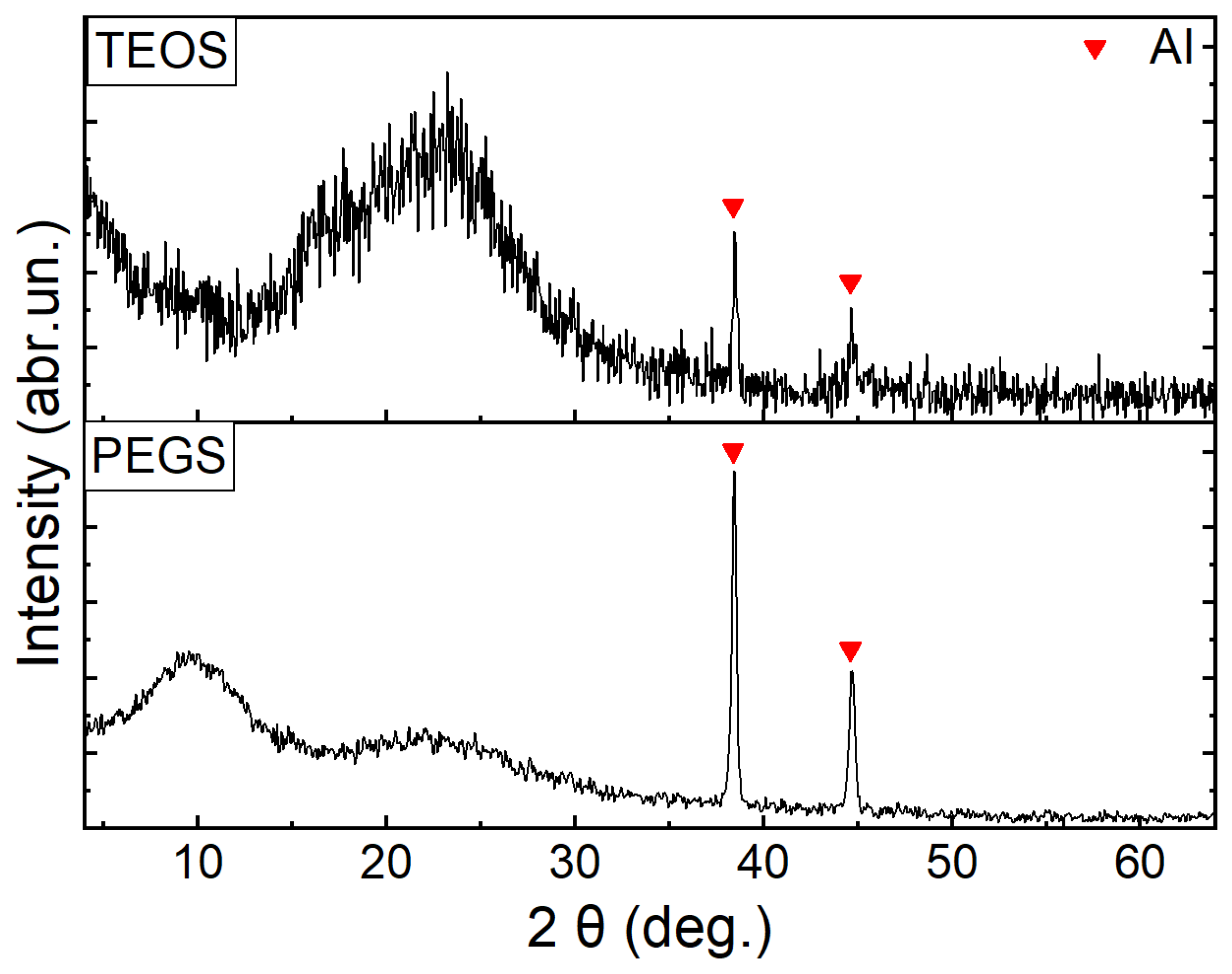
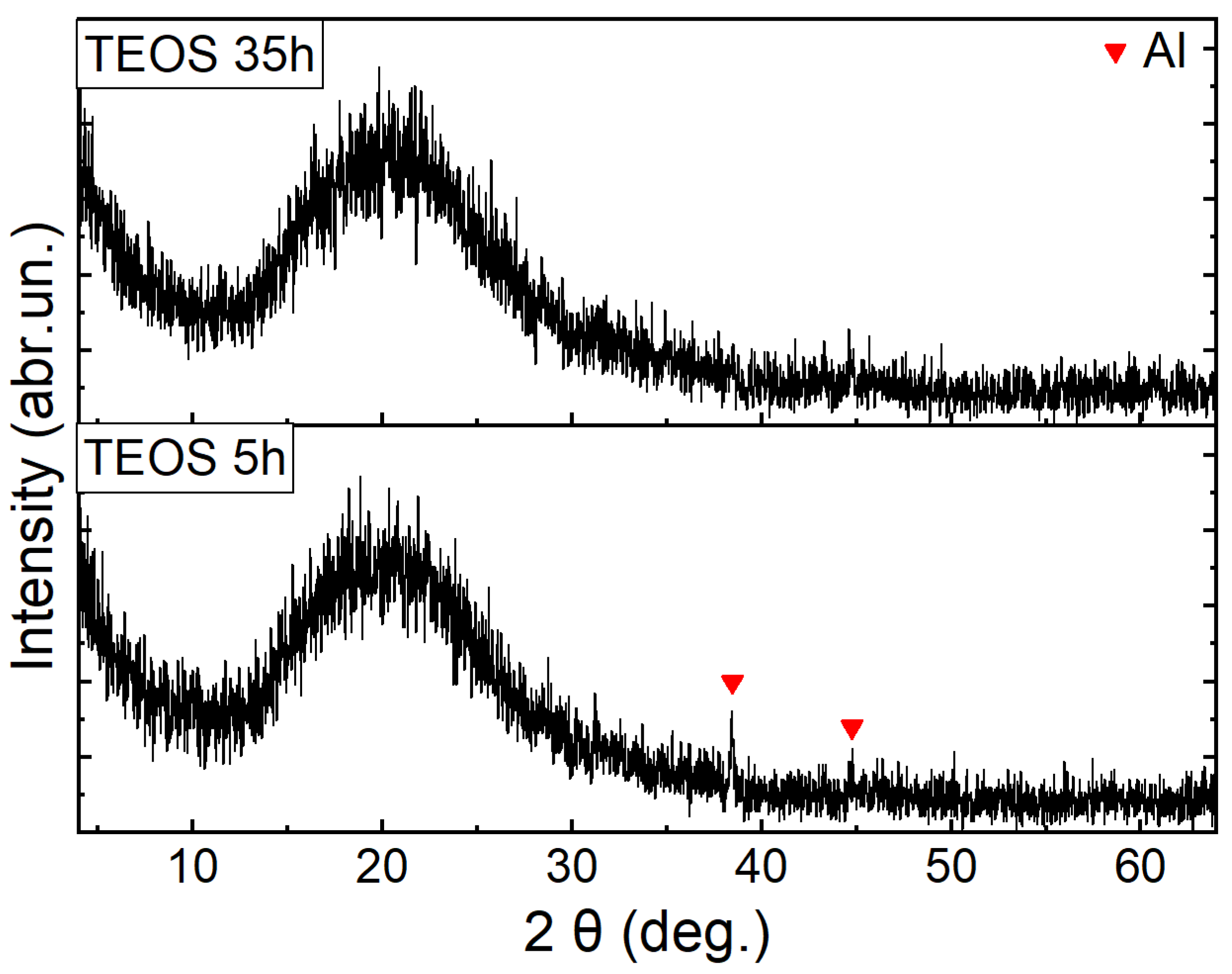
| Powder from TEOS | 44.47 ± 0.36 | 51.19 ± 0.42 | - | 4.34 ± 0.12 |
| Powder from PEGS | 40.58 ± 0.32 | 39.54 ± 0.31 | 14.79 ± 0.21 | 5.18 ± 0.15 |
| Crystalline Phase | Annealing Time, h | |||||||
|---|---|---|---|---|---|---|---|---|
| 0 | 5 | 12 | 19 | 35 | 54 | 70 | 81 | |
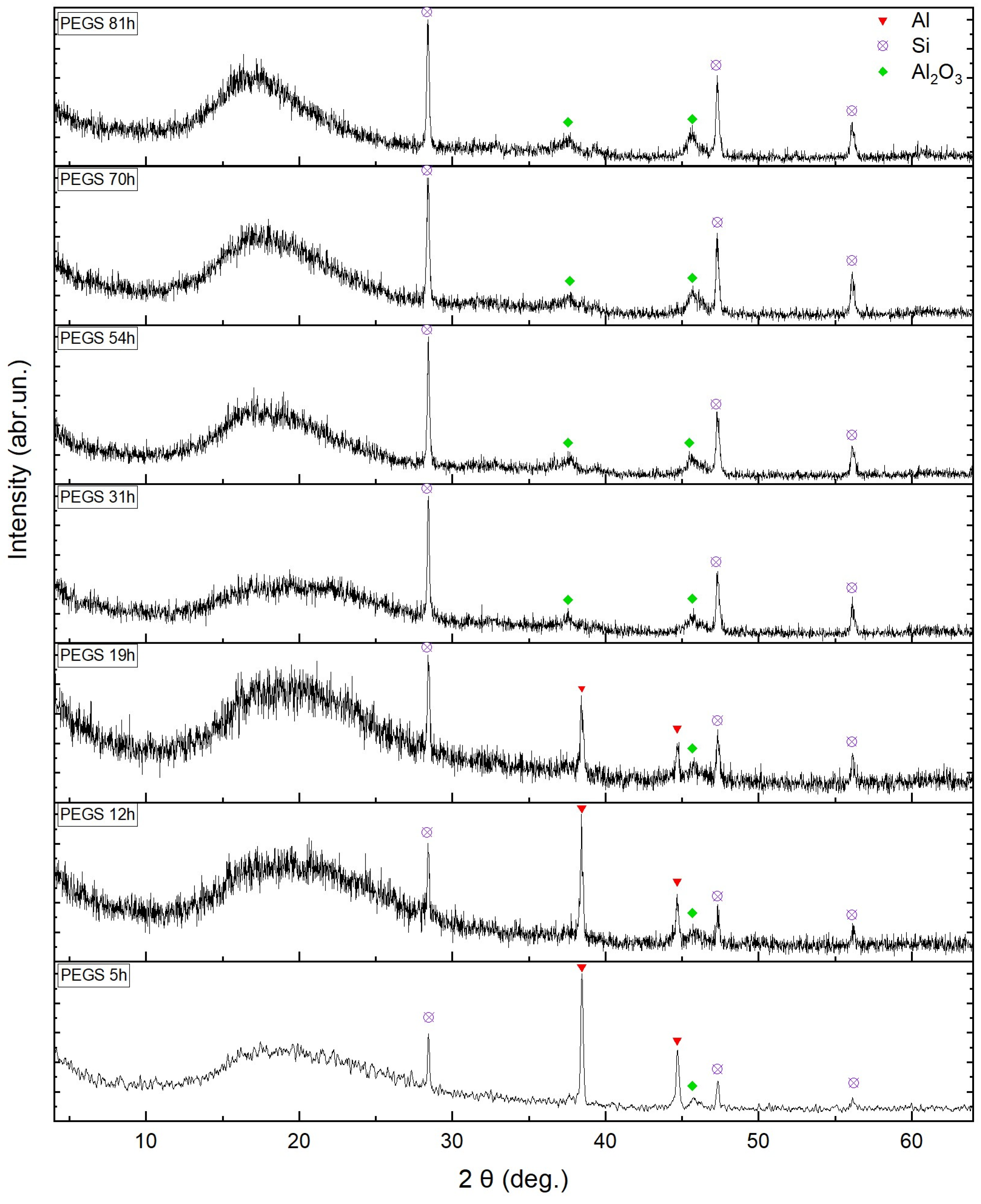
| Al | 5.1 | 4.13 | 2.47 | 1.67 | 0.26 | 0 | 0 | 0 |
| Si | 0 | 0.73 | 1.99 | 2.58 | 3.54 | 3.65 | 3.73 | 3.80 |
| Al2O3 | 0 | 0.77 | 1.33 | 1.46 | 4.68 | 6.74 | 7.26 | 7.79 |
| № p/p | Model | Basic Kinetic Equations | Type (Features) of the Model | Approximation Coefficient R2 |
|---|---|---|---|---|
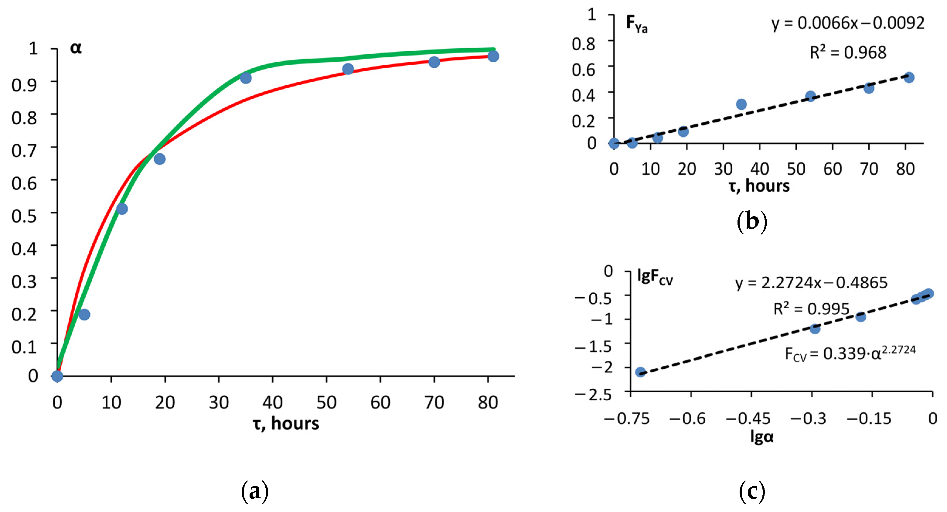
| 1. | Yander | A model of diffusion-controlled reactions. The total reaction rate is determined by the advance of the reagent or its individual components to the reaction interface or the withdrawal of products from it. | 0.978 | |
| 2. | Carter–Valensi | Taking into account the polydispersity of the system: | A diffusion model that takes into account the polydispersity of powders and the difference in equivalent volumes of the coated reagent and the reaction product. | 0.995 (for z = 2) |
| 3. | Tamman | It takes into account the ability of defects in the crystal lattice to cause the reaction, but later their concentration and role decrease, i.e., the rate of disappearance of defects varies inversely with time. | 0.979 | |
| 4. | Ginstling –Braunstein | A decelerating diffusion mechanism with a parabolic law of product layer growth. | 0.935 | |
| 5. | Dunwald –Wagner | The model is based on the assumption that the product is formed by counterdiffusion of interacting reagents through the product layer, i.e., the growth rate of the product is inversely proportional to the thickness of the formed layer. | 0.964 | |
| 6. | Avrami–Yerofeyeva | It takes into account that the limiting stage of solid-phase interaction is the formation (or growth) of product nuclei. | 0.964 (for n = 1) 0.860 (for n = 2) 0.752 (for n = 3) | |
| 7. | Prout –Tompkins | A model for chain type reactions. | 0.892 |
Disclaimer/Publisher’s Note: The statements, opinions and data contained in all publications are solely those of the individual author(s) and contributor(s) and not of MDPI and/or the editor(s). MDPI and/or the editor(s) disclaim responsibility for any injury to people or property resulting from any ideas, methods, instructions or products referred to in the content. |
© 2024 by the authors. Licensee MDPI, Basel, Switzerland. This article is an open access article distributed under the terms and conditions of the Creative Commons Attribution (CC BY) license (https://creativecommons.org/licenses/by/4.0/).
Share and Cite
Cherkashina, N.I.; Pavlenko, V.I.; Gorodov, A.I.; Ryzhikh, D.A. Preparation of Polycrystalline Silicon by Metal-Induced Crystallization of Silicon–Carbon Powder. Ceramics 2024, 7, 989-1001. https://doi.org/10.3390/ceramics7030064
Cherkashina NI, Pavlenko VI, Gorodov AI, Ryzhikh DA. Preparation of Polycrystalline Silicon by Metal-Induced Crystallization of Silicon–Carbon Powder. Ceramics. 2024; 7(3):989-1001. https://doi.org/10.3390/ceramics7030064
Chicago/Turabian StyleCherkashina, Natalia Igorevna, Vyacheslav Ivanovich Pavlenko, Andrey Ivanovich Gorodov, and Dar’ya Aleksandrovna Ryzhikh. 2024. "Preparation of Polycrystalline Silicon by Metal-Induced Crystallization of Silicon–Carbon Powder" Ceramics 7, no. 3: 989-1001. https://doi.org/10.3390/ceramics7030064
APA StyleCherkashina, N. I., Pavlenko, V. I., Gorodov, A. I., & Ryzhikh, D. A. (2024). Preparation of Polycrystalline Silicon by Metal-Induced Crystallization of Silicon–Carbon Powder. Ceramics, 7(3), 989-1001. https://doi.org/10.3390/ceramics7030064


