Article

The Experimental and Modeling Study of Femtosecond Laser-Ablated Silicon Surface

Department of Mechanical Engineering, National Yang Ming Chiao Tung University, No. 1001, Ta Hsueh Road, Hsinchu 300, Taiwan
*
Author to whom correspondence should be addressed.
J. Manuf. Mater. Process. 2023, 7(2), 68; https://doi.org/10.3390/jmmp7020068
Submission received: 10 January 2023 / Revised: 13 March 2023 / Accepted: 15 March 2023 / Published: 16 March 2023

Abstract

:
In this study, monocrystalline silicon was ablated by a single 1030 nm femtosecond laser pulse. Variable laser fluence (0.16–3.06 J/cm2) was used, and two ablation thresholds (0.8 and 1.67 J/cm2) were determined experimentally. A two-temperature model was established based on the dynamic optical model, the carrier density model, and the phase explosion model for comparison with experimental results. The melting (0.25 J/cm2) and vaporization (0.80 J/cm2) thresholds were determined when the lattice temperature reached melting and boiling points, so as to overcome the latent heat. Finally, the ablation depth was calculated using the phase explosion model, and the ablation threshold was 1.5 J/cm2. The comparisons show that the proposed model can predict the ablation depth obtained by a single femtosecond laser pulse.

1. Introduction

The femtosecond laser has attracted significant attention in research, given its features of minimal heat-affected zones and precision machining, as well as its wide range of applications on various materials. In practical use, re-crystallization [1] and surface texturing [2,3,4,5] can be conducted in a relatively low-fluence regime, while micro-machining [6,7] and cutting [8] can be conducted in higher-fluence regimes. According to the high peak power intensity, silicon and dielectric materials can also be machined by a non-linear absorption process [9].
There have been many experimental and theoretical studies on femtosecond laser irradiation on silicon (Si). For experimentation, the ablation threshold, surface morphology, and physical/chemical properties have been investigated using different laser parameters, such as wavelength, pulse duration, and laser pulse numbers [10,11,12,13,14,15,16]. Bonse et al. [10] used an 800 nm femtosecond laser to irradiate Si with different pulse numbers, and proposed the modification threshold and the ablation mechanism. Borowiec et al. [11] used scanning electron microscopy (SEM), transmission electron microscopy (TEM), and atomic force microscopy (AFM) to measure the Si ablated by a single femtosecond laser pulse. The ablation threshold was defined in terms of the removal of materials observed by SEM. Moreover, they also proposed that no extended defects were found regardless of whether low fluence or high fluence was used. Sikora et al. [12] used a picosecond laser of different wavelengths (343, 515, and 1030 nm) to irradiate Si; the ablation thresholds were 0.01, 0.15, and 0.83 J/cm2, respectively. Zayarny et al. [13] used two different wavelengths (515 and 1030 nm) with varied pulse durations (0.2–12 ps) to process Si. They found that the ablation threshold is irrelevant to pulse duration at a 515 nm wavelength. However, at a 1030 nm wavelength, the ablation threshold was 0.9 J/cm2 when the pulse duration was 12 ps. When the pulse duration was decreased to 0.2 ps, the ablation threshold was decreased to around 0.32 J/cm2. The two-photon absorption effect was significantly affected during lasing. Agranat et al. [14] proposed the melting and ablation threshold of Si and GaAs by using a femtosecond laser with a wavelength of 1240 nm. The melting and ablation thresholds of silicon were 0.2 and 0.33 J/cm2, respectively. Hwang et al. [15] investigated the ablation efficiency by using a single 800 nm femtosecond laser to ablate silicon. Two ablation regimes were proposed, and the two ablation thresholds were 0.458 and 0.637 J/cm2. The ablation efficiency started to decrease when the fluence was higher than 10 J/cm2. The air plasma absorbed the laser energy and caused the ablation efficiency to decrease. Ionin et al. [16] used different fluences to machine Si and proposed melting, spallation, and fragmentation thresholds. Smirnov et al. [17] investigated ablation efficiency in different mediums (air and water). A 515 nm single-pulse femtosecond laser was used to irradiate silicon. The ablation efficiency in the air decreased with decreased pulse duration, and vice versa.
In theory, the Boltzmann transport equation with the two-temperature model (TTM) can describe the laser–silicon interaction. Van Driel et al. [18] examined the phenomenon of Si excited by IR and green picosecond lasers, and the behavior of the melting threshold under varied pulse durations. They observed that the melting threshold did not vary significantly with pulse duration in green wavelengths, while in IR wavelengths, the pulse duration significantly influenced the melting threshold due to the two-photon absorption and free-carrier absorption effect. Chen et al. [19] investigated the temporal carrier density, electrons, and lattice temperature. They predicted melting thresholds under different pulse durations, supported by experimental results. In addition, the Drude model was added to describe the dynamic optical properties and enhance the accuracy. Rämer et al. [20] compared the dynamic optical properties calculated by three different electron–phonon collision frequencies and determined the melting threshold. Their predicted melting threshold matched with the experimental results when the collision frequency was temperature-dependent.
Although many studies have discussed the laser–silicon interaction, there is no consensus on the definition of melting and ablation thresholds. For the melting threshold, some studies found that Si melts when the carrier density reaches a critical density [19,21]. The problem of melting latent heat should be solved [18]. In fact, the lattice temperature reaching the melting temperature was also considered to be a melting threshold [20]. For the ablation threshold, Wu et al. [22] proposed that Si is ablated when the lattice temperature reaches the separation temperature. They predicted the ablation depth in a high-fluence regime (5–35 J/cm2), and at the pulse duration of 120 fs, the results agreed with experimental results. Tsibidis et al. [23] predicted the laser-induced periodic surface structures (LIPSS) profile by using the TTM with a hydrodynamic model and a phase explosion model. When the lattice temperature reached 0.9 T c r ( T c r is the critical point temperature), the material was ejected with a mixture of gas and droplets. The ablation depth and the period of LIPSS were consistent with experimental results. Moser et al. [24] compared experimental results and theoretical results by using a 1030 nm femtosecond laser to ablate Si with varied fluence (1–10 J/cm2). They suggested that the Si was ablated when the lattice temperature reached the vaporization temperature, and overcame the latent heat of vaporization. The theoretical results were consistent with the experimental results. Chen et al. [25] used a 2D model to predict the ablation profile, and compared it with experimental results obtained using a 1040 nm femtosecond laser. The ablation condition was used to find the isotherm contour, which was similar in shape to that of the ablation profile. Lastly, ablation occurred when the lattice temperature reached 4975 K. Vaghasiya et al. [26] used TTM with constant optical properties to simulate silicon irradiated by a single green femtosecond laser with a fluence of 0.75 to 9 J/cm2. Two ablation mechanisms were used. One was non-thermal ablation, which occurred when the carrier density reached a critical density; the other was the phase explosion mechanism. Feng et al. [27] used the pump–probe technique to measure the change in dynamic reflectivity under a 1030 nm femtosecond laser, and predicted electron plasma generation and dynamic reflectivity using the TTM and Drude models. They found that the reflectivity evolution depended highly on laser fluence.
In summary, several methods can be used to determine the phase transition and ablation depth. In this study, the carrier density model and TTM with a dynamic optical model were used to describe the phenomenon during lasing and define the phase transition, ablation threshold, and ablation depth. The melting ( m t h ), vaporization ( v t h ), and phase explosion ( p h t h ) thresholds were determined. For m t h and v t h , the phase transition was completed when the lattice temperature reached the melting point ( T m ) and boiling point ( T b ), and overcame the latent heat of melting ( L m ) and vaporization ( L v ), respectively. In the final stage, the phase explosion was considered the ablation mechanism in this study. When the lattice temperature reached 0.9 T c r (7132 K), calculation of the ablation depth began. In the experimental part, a single 1030 nm femtosecond laser pulse was used to ablate Si, and results were compared with the simulation results. The fluence used was around 0.16–3.06 J/cm2.

2. Materials and Modeling Method

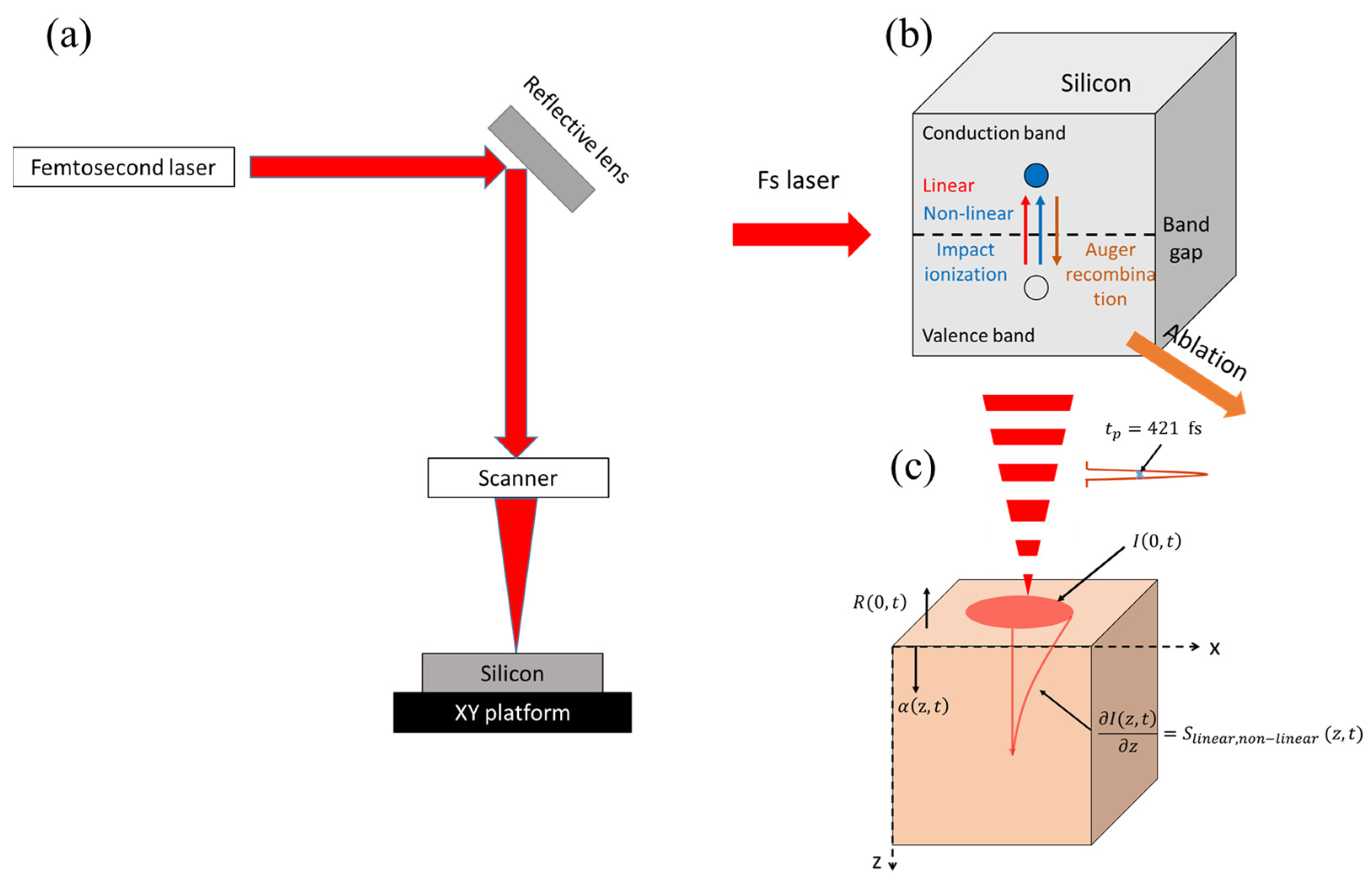
2.1. Experimental Setup and Sample Analysis

Figure 1 presents the schematic of the experimental setup and the process of interaction of the fs laser with the silicon. Polished non-doped monocrystalline Si <111> was used for processing in this study. Figure 1a is the schematic of the experimental system. A fiber femtosecond laser (KASMORO, mRadian Inc, Hsinchu, Taiwan), with a wavelength of 1030 nm, a repetition rate of 100 kHz, a pulse duration of 421 fs (FWHM), and an average laser power of 2 W was used. An electronic shutter was utilized and triggered to conduct the single pulse. The rising/falling time of the shutter provided by the laser company was about 100~200 ns. Therefore, to control only one pulse laser selectively, the switching time of the shutter was set at 16 μs, which is slightly higher than the pulse separation time of 10 μs by repetition rate 100 kHz. The output laser spot size was 2.2 mm. The laser beam was reflected by a series of reflective mirrors and focused by an F-theta lens with f = 100 mm. The sample was mounted on an x–y platform.
Laser power was measured by a power meter (919P-050-26, Newport, Irvine, CA, USA). A laser power of 1.478–0.282 W was used in this study and the pulse energy (0.76–14.78 μJ) was calculated. The effective focal spot size was 35.1 μm, which was determined by the D2 method [28]. The effective input fluence on the sample surface was determined (0.16–3.06 J/cm2). Before experimenting, the profile of the beam focused by the f-theta lens was checked using a beam profiler. The results showed that the beam profile had a near-Gaussian distribution, and no obvious hotspots existed.
After the experiment, the sample was cleaned with deionized water in an ultrasonic bath. Scanning electron microscopy (SEM; Hitachi SU-8010, Tokyo, Japan) and AFM (Bruker ICON, Billerica, MA, USA) were used to measure the ablation profile. The AFM mapping area was 50 × 50   μ m . After checking all AFM data, the deepest point in the mapping area was considered the ablation depth.

2.2. The Modeling

When using a femtosecond laser to irradiate the Si, electron–hole pairs were generated by a single- or two-photon absorption process, depending upon the photon energy and the bandgap energy. The electron in the conduction band absorbs the photon energy and causes the free-carrier absorption. At the same time, a part of the electron in the conduction band recombines via the Auger process, and some new electron pairs are generated by impact ionization. The Boltzmann transport equation and TTM were used to describe the process [18]. The schematic of electron–hole generation during femtosecond laser irradiation is shown in Figure 1b.
To calculate the carrier density ( n e ) in the conduction band, the single- and two-photon absorptions, Auger recombination, impact ionization, and ambipolar diffusion must be considered:
n e t = α I z , t h ω + β I z , t 2 2 h ω γ n 3 + θ n e D 0 n e
In Equation (1), the first two terms on the right-hand side represent the single- and two-photon absorptions. The third ( γ n 3 ) and fourth terms ( θ n e ) denote the Auger recombination and impact ionization, respectively. The final terms denote carrier diffusion. Here, I is the laser intensity, h ω is the photon energy, α and β are the single- and two-photon absorption coefficients, respectively, γ is the Auger recombination coefficient, θ is the impact ionization coefficient, and D 0 is the ambipolar diffusion coefficient.
In the femtosecond laser process, the temporal evolution of the electron and lattice temperature was described using the TTM [18]. In semiconductors, the dynamic carrier density and the varied bandgap energy must be considered in the TTM, as shown below:
C e T e t = · K e T e G T e T l + S z , t n e t E g + 3 K B T e n e E g n e n e t + E g T l T l t
C l T l t = · K l T l + G T e T l  
In Equations (2) and (3), C is the heat capacity, K is the heat conductivity, G is the coupling factor, S is the laser heat source term, E g is the bandgap energy, and the K B is the Boltzmann constant. Subscript e and l represent the electron and lattice, respectively. The thermal parameters used in Equations (2) and (3) need to be modified when the phase changes. In the liquid state, the heat capacity and heat conductivity were modified. However, there were no measurement data for these parameters in the vapor state; hence, the parameters of the liquid state were used to simulate the subsequent heating process in the vapor state.
When a laser irradiates the sample surface, a part of the laser intensity is reflected by the sample surface, while another part of the laser intensity is absorbed and propagated into the sample with exponential decay. However, when a femtosecond laser irradiates Si, electrons absorb the photon energy and increases the kinetic energy, thereby causing an electron–electron collision and inducing changes in the optical properties. The dynamic optical properties must, therefore, be considered. After that, the temporal laser heat source that is propagated into the sample can be calculated. The schematic of the laser absorption process is shown in Figure 1c. In general, the Drude model can be used to simulate the dynamic optical properties when the Si is excited by a femtosecond laser. The Drude model is shown below [22]:
ε = 1 + ( ε r 1 ) 1 n e n 0 n e e 2 ε 0 m e ω 2 1 1 + i v / ω  
where ε r is the dielectric constant when the material is at 300 K, n 0 is the electron density of the valance band, e is the electron charge, ε 0 is the permittivity of vacuum, m e is the effective electron mass, ω is the laser frequency, and v is the collision frequency.
After obtaining the dynamic dielectric constant, the refractive index n and extinction coefficient k can be determined by Equations (5) and (6). It is assumed that the laser pulse is normal to the sample (along the z axis), and the dynamic surface reflectivity and free-carrier absorption coefficient can be determined using Equations (7) and (8) [29]:
n = R e ε + R e ε 2 + I m ε 2 2  
k = R e ε + R e ε 2 + I m ε 2 2  
R 0 , t = n 1 2 + k 2 n + 1 2 + k 2
α F C A = 2 ω k c
In Equation (8), c is the speed of light in a vacuum.
Assuming that the laser pulse is normal to the sample surface, the surface laser intensity with dynamic reflectivity can be expressed as Equation (9):
I 0 , t = 0.94 × 1 R 0 , t × F t p · e x p 2.77 t t p 2  
where R 0 , t is the surface reflectivity determined by Equation (7), F is the laser fluence, and t p is the FWHM pulse duration of a Gaussian pulse.
When the laser intensity propagates into the material along the z axis, the laser attenuation can be obtained by solving the following ordinary differential equation:
I z , t z = α S P A + α F C A I β I 2
where α S P A is the single-photon absorption coefficient, α F C A is the free-carrier absorption coefficient obtained by Equation (8), and β is the two-photon absorption coefficient.
In summary, the total laser heat source term described in Equation (2) can be expressed as follows:
S z , t = α t o t a l I z , t
where α t o t a l is the α S P A + α F C A shown in Equation (10) and I z , t is the intensity along the z axis depending on the dynamic optical properties.
In this study, the intermediate regions of the solid–liquid and liquid–vapor interfaces were neglected for convenience of calculation. For the criteria of melting and vaporization thresholds, we considered that when the lattice temperature ( T l ) reaches melting ( T m ) and boiling temperatures ( T b ), and the latent heat of melting ( L m ) and vaporization ( L v ) can be overcome, respectively, the material transitions from solid to liquid and liquid to vapor. It is noted that when the lattice temperature reaches T m or T b but L m and L v are not yet overcome, the lattice temperature can be set at T m or T b . The lattice temperature increases again when L m and L v are overcome.
A previous study [30] proposed that phase explosion is the primary ablation mechanism in the femtosecond regime. Thus, in this study, phase explosion was considered the main ablation mechanism. When T l reached 0.9 T c r , calculation of the ablation depth began. All the thermal and optical parameters used in this study are shown in Table 1.
In the numerical simulation, the thickness of the material was set at 5 μm which is larger than the carrier diffusion depth (3 μm) [18]. The number of grids was 1000, and the grid size was 5 nm. The 1D finite difference method was used in this study [19]. The initial electron, lattice temperature, and carrier density were set at 300 K and 1 × 10 12   cm 3 , respectively. The plasma shielding effect was not considered in this study.

3. Results and Discussion

In this section, the experimental results and simulation results are compared. For experimentation, the fluence used was 0.16–3.06 J/cm2. The two ablation thresholds were obtained by the relationship between laser fluence and ablation depth. In the modeling part, first, the thresholds of melting ( m t h ) , vaporization ( v t h ) , and phase explosion ( p h t h ) were proposed. Then, the temperatures of the electron ( T e ) and lattice ( T l ) , the carrier density ( n e ) , and the dynamic optical properties ( R and α F C A ) were proposed. Here, the fluence used to calculate the ablation depth was 1.50–3.06 J/cm2. Finally, the ablation depth determined by modeling was compared with the experimental results.

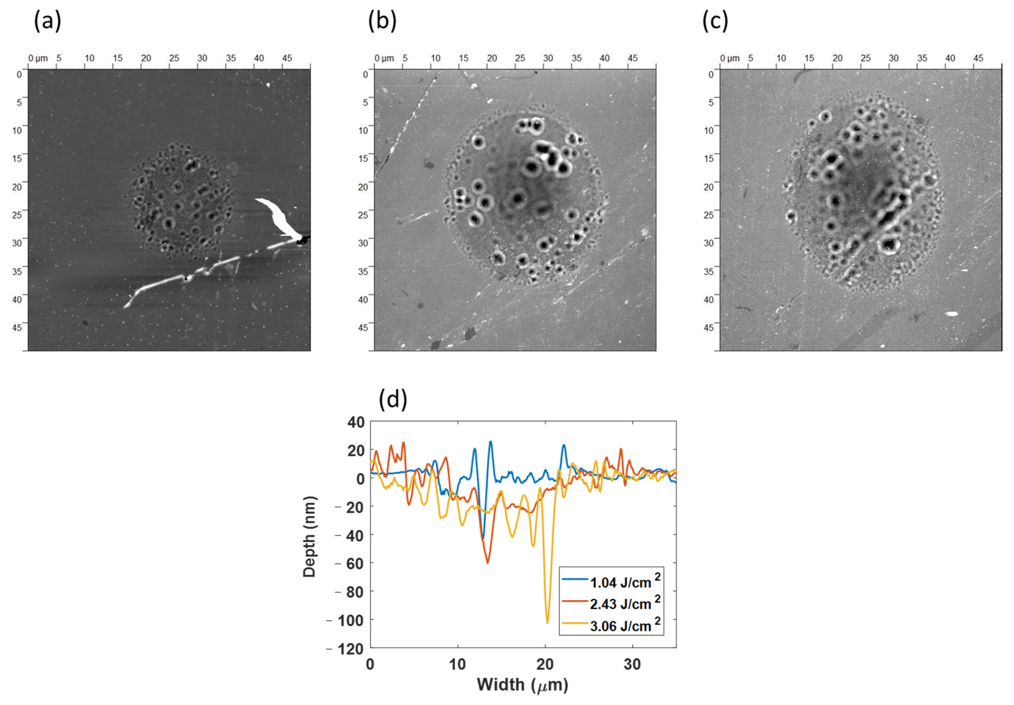
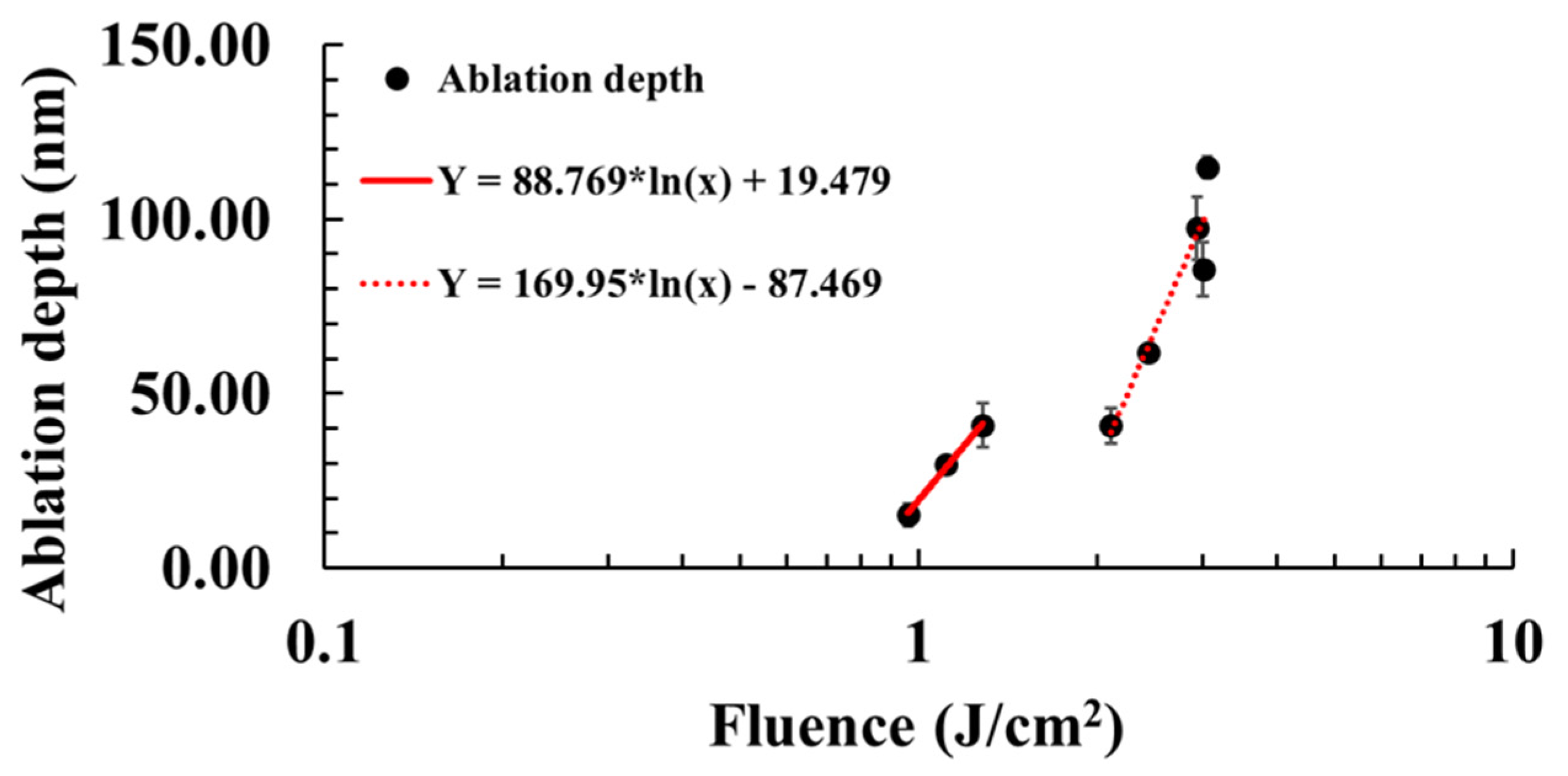
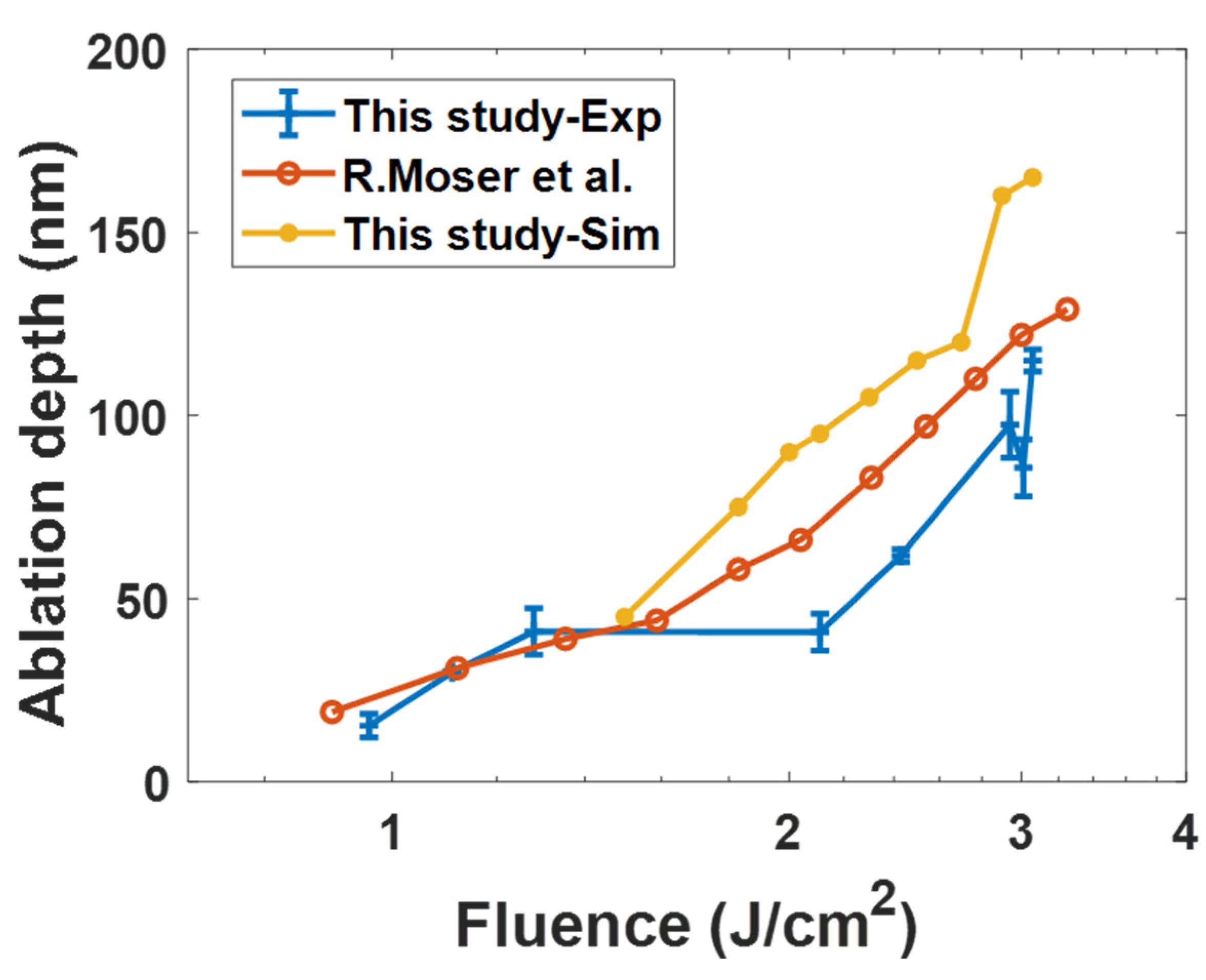
3.1. Experimental Results

Figure 2 presents the 3D AFM images, and the crater profiles obtained by laser fluence were 1.04, 2.43, and 3.06 J/cm2. The width and depth of the crater increased with the increase in fluence. The deepest ablation depth was around 110 nm. Some small holes were observed in the laser-irradiated area; the phenomenon was similar to that reported previously [10]. When the Si absorbs the laser intensity, the surface layer is overheated and removed by phase explosion. The remaining liquid layer underwent normal boiling, and inhomogeneous nucleation bubbles occurred simultaneously [33].
As shown in Figure 3, some nanoparticles existed on the sample surface, which might affect the ablation process in a low-fluence regime and cause misestimation. This study, thus, adopted an ablation depth above 10 nm for analysis. Referring to the previous results [24,34], the ablation depth was plotted as a function of input laser fluence. Figure 3 shows the semi-logarithmic plot of the ablation depth against the laser fluence. The experimental data indicated that the curve fitting resulted in two straight lines, which can be defined as two different ablation regimes [24]. The ablation threshold can also be determined when y is set to zero. The two ablation thresholds were 0.8 and 1.67 J/cm2. The ablation depth and the ablation threshold are similar to those in earlier published results [24]. In the lower-fluence regime, the slope of the fit function (solid line) corresponded to the optical penetration depth, which is about 49 nm, and close to the previous results of 52 nm [24]. On the other hand, when the fluence increased, the penetration depth was driven by electron heat diffusion. Therefore, the effective penetration depth increased to 135.85 nm, which is also close to the previous results of 135 nm [24].

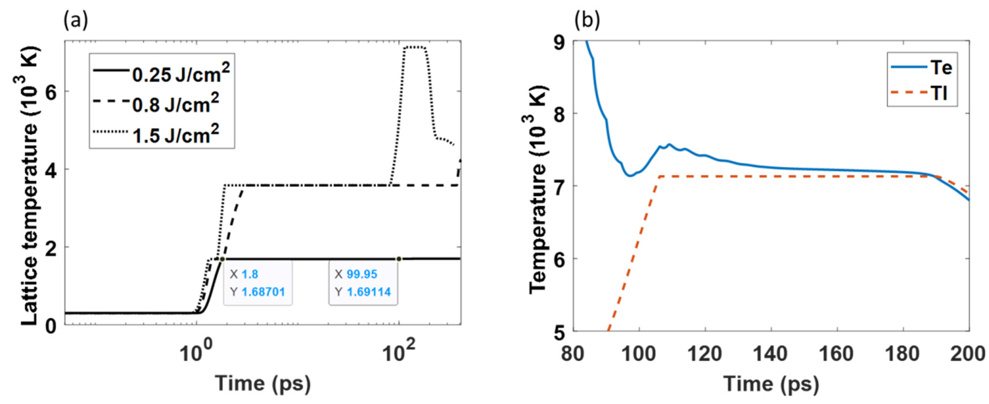
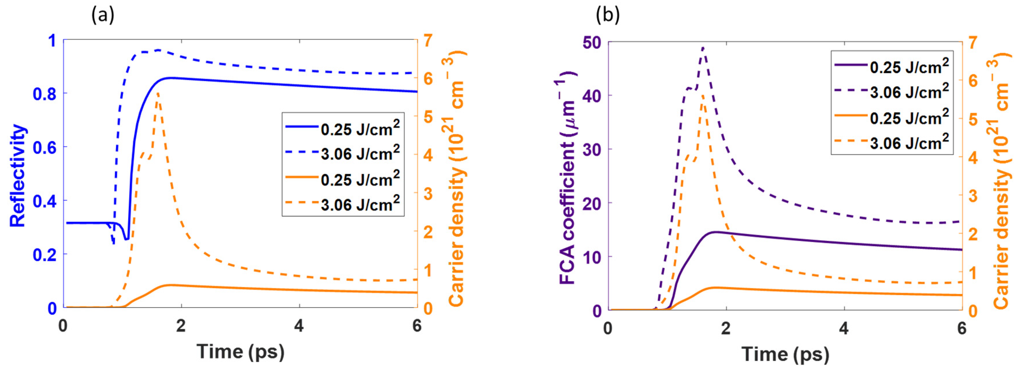
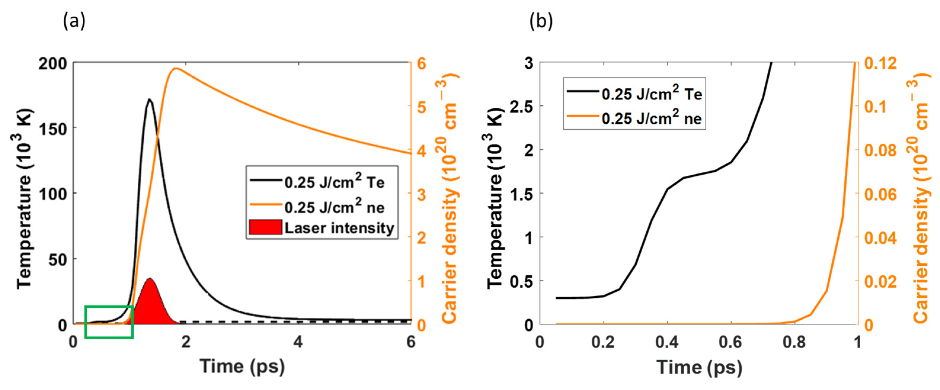
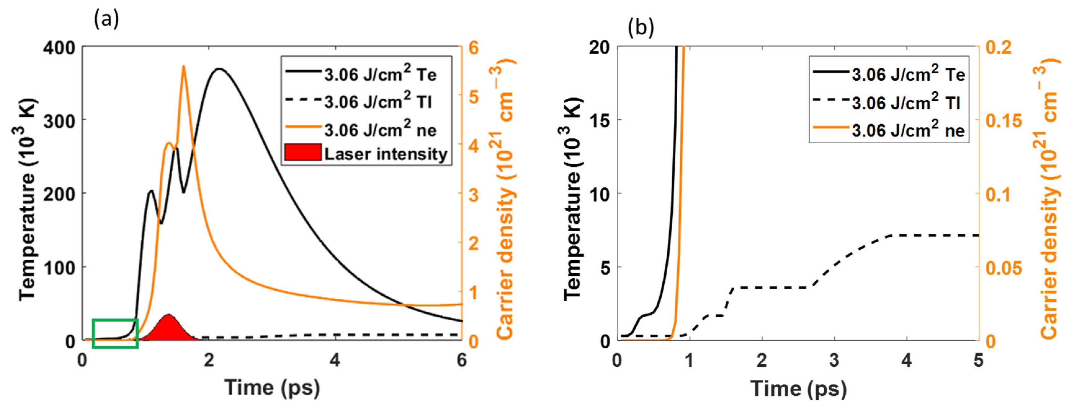
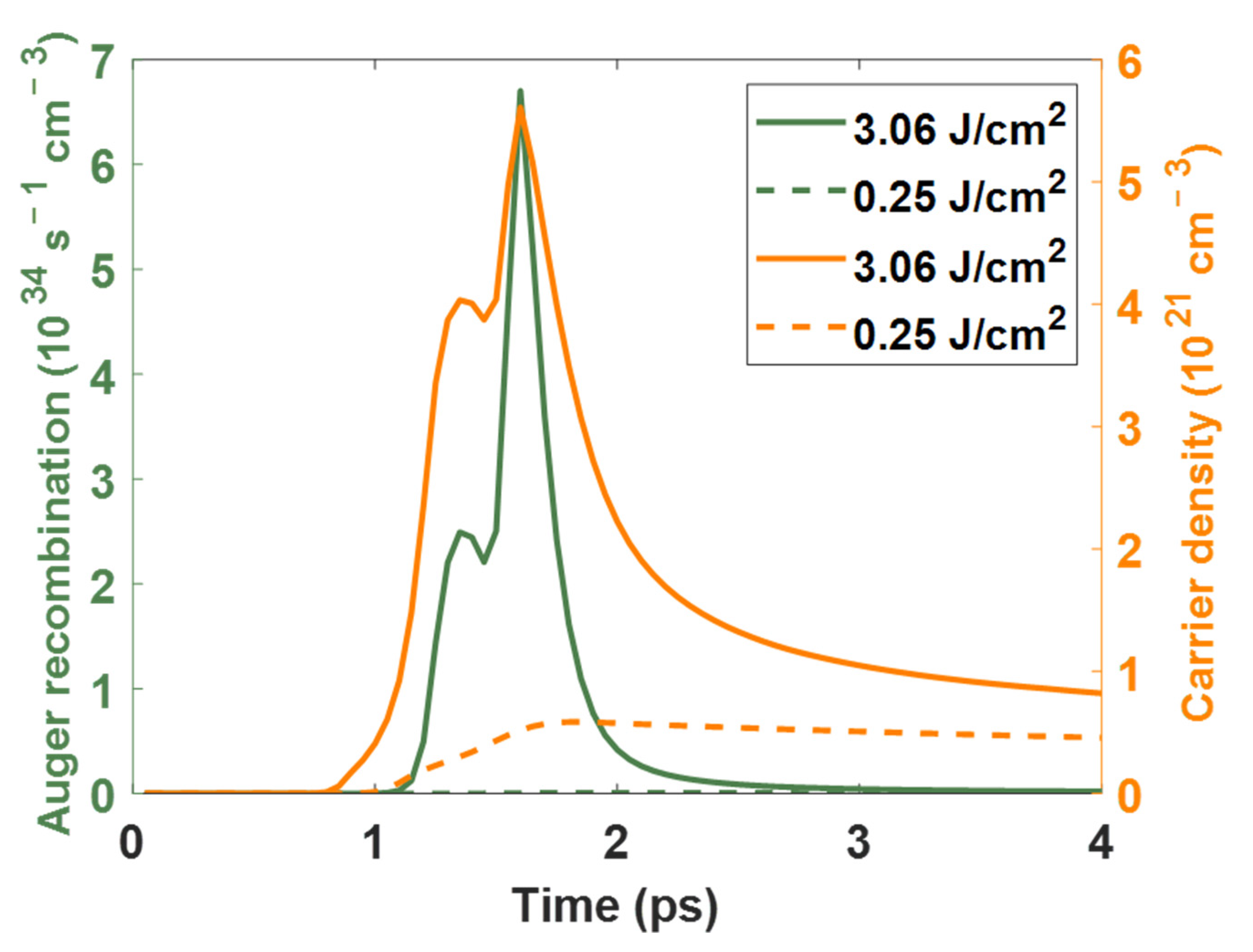
3.2. Simulation Results

In this section, the temporal properties of n e ,   T l , and   T e as well as the optical properties were calculated by Equations (1)–(8) with different input fluences. Figure 4a presents the time evolution of T l on the front surface of the sample, which was calculated with fluences 0.25, 0.8, and 1.5 J/cm2. These three fluences represented m t h , v t h , and p h t h , respectively. The two square spots shown in Figure 4a represent the timing of T l reaching T m at 1.8 ps, and overcoming L m at 99.95 ps when the fluence was 0.25 J/cm2. After that, the silicon transitioned to a liquid state and the lattice temperature increased again. When the fluence was 0.8 J/cm2, T l overcame L m and L v at 1.85 ps and 373.6 ps, respectively. The material transitioned from solid to liquid and from liquid to vapor. When the fluence was 1.5 J/cm2, as shown in Figure 4b, T l overcame L m and L v at 1.3 ps and 82 ps, respectively. Then, T l increased again and reached 0.9   T c r (7132 K) at 115 ps. At that time, phase explosion began, and the ablation depth was calculated. At 179.7 ps, T l started to decrease as the thermal equilibrium was established. T l decreased with T e .
After obtaining the threshold of the phase transition by the proposed model, we compared the simulation results with the experimental results. First, for the melting threshold, the m t h (0.25 J/cm2) calculated by the simulation in this study was matched with previously published results (0.26 J/cm2 [10] and 0.27 J/cm2 [35]). The v t h (0.80 J/cm2) was matched with the threshold (0.80 J/cm2) mentioned in Section 3.1. The p h t h (1.5 J/cm2) calculated in this study was close to the threshold (1.67 J/cm2) obtained in our experiments. The threshold of phase transition obtained by simulation was in good agreement with the experimental results.
Figure 5 presents the temporal evolution of the reflectivity, free-carrier absorption ( α F C A ), and n e obtained by two different fluences. As shown in the figure, n e is highly different between the two fluences. When a high fluence was used to excite the Si, there were more electrons transiting from the valance band to the conduction band, and more free carriers were generated to induce higher n e . As shown in Figure 5a, the reflectivity was highly associated with n e . When n e started to increase, the reflectivity decreased to a minimum. As n e reached its maximum and began to drop, the reflectivity also reached a maximum and started to decrease. When the fluence was 0.25 J/cm2, the reflectivity decreased to 0.25 at 1.05 ps, and increased to 0.85, and then decreased slowly. However, when the fluence was 3.06 J/cm2, the reflectivity decreased to a minimum at 0.85 ps and increased quickly to 0.95, and slowly decreased. On the other hand, α F C A had a strong correlation with n e . Irrespective of the fluence used to excite the Si, the upward and downward trends of α F C A were similar to those for n e . Because more free-carriers were generated at a high fluence, the maximum of α F C A had a distinct difference. At a low fluence, the results of dynamic reflectivity and α F C A were similar to those mentioned in previous studies [20].
Although the trend of the reflectivity was similar to previous results, the maximum reflectivity (0.8 and 0.95) calculated by the Drude model used in this study was higher than results (0.72) in other studies [36,37], which were obtained by the pump–probe method. It can be explained by the following reasons: First, the bandgap renormalization effect, which could enhance the interband transition and cause more electron transition from the valance band to the conduction band [37], was not considered in this study. Second, the ambipolar diffusion coefficient D 0 used in this study was dependent on the lattice temperature. However, according to an earlier publication [38], the ambipolar diffusion coefficient varied with n e . D 0 can reach 10–100   cm 2 / s when n e = 10 20 10 21   cm 3 . Therefore, the temporal carrier density calculated in this study was slightly misestimated; thus, the reflectivity was higher than the experimental results [36,37].
Figure 6 presents the time evolution of T e and n e obtained with a fluence of 0.25 J/cm2. The magnified green square in Figure 6a is presented in Figure 6b. As shown in Figure 6b, T e started to increase and reached a plateau at 0.4 ps. Then, at 0.6 ps, T e increased significantly and reached a maximum at 1.3 ps as shown in Figure 6a. After that, T e decreased with the decrease in laser intensity. The phenomenon was similar to previous results [20]. Single-photon absorption caused the first increase. At this moment, the bandgap was not overcome. For the second increase, the two-photon absorption and the free-carrier absorption processes dominated the laser intensity and caused a dramatic increase in T e . On the other hand, n e varied with the laser intensity; it reached a maximum at 1.8 ps, which is slightly slower than the point at which laser intensity reached its maximum, and then decreased slightly. The maximum was 6 × 10 20   cm 3 . The trajectory of T e and n e was similar to those mentioned in previous studies [19,20]. However, the maximum of n e was lower than that in previous studies [19,20] due to the difference in laser wavelengths (1030 nm (this study) and 800 nm [19,20]) used to simulate the laser–silicon interaction. At 300 K, the single-photon absorption was quite different between 1030 nm (29 cm−1) and 800 nm (827 cm−1) [39] conditions for Si, so n e obtained at 1030 nm was lower than obtain at 800 nm using the same fluence.
Figure 7 presents the time evolution of T e , T l , and n e obtained at 3.06 J/cm2. Figure 7b is the magnification of the green square in Figure 7a. As shown in Figure 7a, the upward trend of T e and n e differed from those at 0.25 J/cm2. Three peaks were observed at 1.1, 1.5, and 2.15 ps. At the early stage of the laser pulse, as shown in Figure 7b, T e reached a plateau at 0.3 ps, and then increased again until reaching a maximum at 2.15 ps. After that, T e started to decrease because the laser pulse was complete. During the upward trend of T e , T e decreased twice at 1.25 and 1.6 ps. At 1 ps, as shown in Figure 7b, the lattice temperature started to increase. It can be deduced that the electron–lattice coupling effect caused the decrease in T e . Particularly, n e significantly influenced T e when n e was greater than 4.0 × 10 21   cm 3 . When n e decreased, T e increased. After n e reached a second peak at 1.6 ps and started to decrease, the laser pulse domain showed an upward trend in T e .
On the other hand, as shown in Figure 7b, T l began increasing, reached T m , and overcame L m at 1.45 ps. After that, T l started to increase again, overcame L v at 2.65 ps, and finally, reached 0.9 T c r . At that time, the silicon started to be ablated.
Comparing Figure 6a and Figure 7a, the upward trajectory of n e was highly different between 0.25 and 3.06 J/cm2 conditions. According to Equation (1), the laser intensity and the Auger recombination effect ( γ n 3 ) dominate the increase in n e . It should be noted that the detailed physical mechanism of the Auger recombination process is not completely understood in the high-carrier-density regime. Figure 8 presents the γ n 3 and n e calculated by different fluences. The results show that when the fluence was 0.25 J/cm2, the maximum of γ n 3 was 7.4 × 10 31   s 1 cm 3 and was insufficient to influence the increase in n e . On the contrary, when the fluence increased to 3.06 J/cm2, the γ n 3 was gradually influenced by the upward trend of n e . The upward trajectory of n e and γ n 3 were similar to each other. Two peaks were observed at 1.3 and 1.6 ps. The maximum of γ n 3 was 6.7 × 10 34   s 1 cm 3 . After reaching the maximum point, n e and γ n 3 decreased together. Therefore, we deduced that the laser intensity dominated the increase in n e when the fluence was 0.25 J/cm2. On the other hand, in addition to the laser intensity, γ n 3 influenced n e when the fluence was 3.06 J/cm2.
Figure 9 shows the comparison of simulation and experimental ablation depths. In the low-fluence regime (<1.28 J/cm2), the ablation depth obtained by our experiment is consistent with a previous study [24]. The error increased with increased fluence; nevertheless, the increasing trend was similar. It should be noted that the ablation threshold was 1.5 J/cm2 when the phase explosion model was used in this study. Thus, no ablation depth was calculated when the fluence was below 1.5 J/cm2. The ablation depth increased linearly for 1.5–2.7 J/cm2. When the fluence was increased above 3 J/cm2, the calculated ablation depth increased significantly. The maximum ablation depth was 165 nm when the fluence was 3.06 J/cm2. Obviously, the simulation results are in line with previous results [24] when the fluence was set at 1.5–2.7 J/cm2.
However, when the fluence was greater than 3.0 J/cm2, the error increased. This was possibly due to two reasons. First, a 1D model was used in this study, and the heat was only propagated along the z axis. This may have caused an overestimation of the ablation depth when the fluence increased. Second, the plasma shielding effect was not considered in this study. When a laser with high fluence was irradiated on the sample surface, early plasma was generated by hot electron emission. The plasma absorbed the incident laser energy, thus reducing the actual laser energy. A previous study [40] reported that when the fluence was set at 3 J/cm2, early plasma started to absorb the laser energy. However, in this study, ideal fluence was used in the proposed model; thus, the error in the high-fluence regime was increased. Third, when the fluence was higher than 3 J/cm2, the hydrodynamic motion of molten silicon was the key factor in influencing the ablation process [24]; however, the proposed model did not consider the hydrodynamic motion, so the ablation depth was possibly overestimated. When the phase explosion was considered the main ablation mechanism, the calculated ablation depths matched the experimental results in the range of 1.5–2.7 J/cm2.

4. Conclusions

Single femtosecond laser pulse ablation of Si was conducted with different fluences (0.16–3.06 J/cm2) and the experimental and simulation results were reported. The phenomenon during lasing was described using the carrier density and TTM with a dynamic optical model. The numerical simulation determined the melting, vaporization, and phase explosion thresholds. The phase explosion model was used to determine the ablation depth. The results can be concluded as follows:
  • Two different ablation thresholds obtained by the relationship between laser fluence and ablation depth were nearly 0.84 and 1.67 J/cm2;
  • The melting, vaporization, and phase explosion thresholds determined by the numerical simulation were 0.25, 0.8, and 1.5 J/cm2, respectively;
  • Comparing the simulation results obtained using the fluences of 0.25 and 3.06 J/cm2, a higher laser intensity caused a greater electron transit from the valence band to the conduction band. The Auger recombination effect highly influenced the carrier density in a high-fluence regime;
  • The dynamic reflectivity and free-carrier absorption varied with carrier density. The free-carrier absorption coefficient obtained at high fluences was higher than that obtained at low fluences and caused a higher electron temperature at high fluences;
  • The simulation results from the phase explosion model were in line with the experimental results in a moderate-fluence regime.

Author Contributions

Conceptualization, C.-W.C. and Y.-H.L., supervision; C.-W.C. and Y.-H.L., proposed the concept and designed the experiment; Y.-H.L. contributed to the measurement results; Y.-H.L. and C.-W.C. wrote the original draft. Y.-H.L. and C.-W.C. contributed to the simulation results. C.-W.C. funding acquisition. All authors have read and agreed to the published version of the manuscript.

Funding

This work was supported by the Ministry of Science and Technology of the Republic of China under contract no. MOST 110-2221-E-A49-110.

Data Availability Statement

Not applicable.

Acknowledgments

This work was supported by the Ministry of Science and Technology of the Republic of China under contract no. MOST 110-2221-E-A49-110.

Conflicts of Interest

The authors declare no conflict of interest.

References

  1. Florian, C.; Fischer, D.; Freiberg, K.; Duwe, M.; Sahre, M.; Schneider, S.; Hertwig, A.; Krüger, J.; Rettenmayr, M.; Beck, U. Single femtosecond laser-pulse-induced superficial amorphization and re-crystallization of silicon. Materials 2021, 14, 1651. [Google Scholar] [CrossRef]
  2. Zhao, J.H.; Li, X.B.; Chen, Q.D.; Chen, Z.G.; Sun, H.B. Ultrafast laser-induced black silicon, from micro-nanostructuring, infrared absorption mechanism, to high performance detecting devices. Mater. Today Nano 2020, 11, 100078. [Google Scholar] [CrossRef]
  3. Borodaenko, Y.; Gurbatov, S.; Tutov, M.; Zhizhchenko, A.; Kulinich, S.A.; Kuchmizhak, A.; Mironenko, A. Direct Femtosecond Laser Fabrication of Chemically Functionalized Ultra-Black Textures on Silicon for Sensing Applications. Nanomaterials 2021, 11, 401. [Google Scholar] [CrossRef]
  4. Liu, Y.; Ding, Y.; Xie, J.; Chen, M.; Yang, L.; Lv, X.; Yuan, J. Research on Monocrystalline Silicon Micro-Nano Structures Irradiated by Femtosecond Laser. Materials 2022, 15, 4897. [Google Scholar] [CrossRef] [PubMed]
  5. Liu, Y.-H.; Kuo, K.-K.; Cheng, C.-W.; Lee, A.-C. Femtosecond laser two-beam interference applied to 4H-SiC surface hierarchical micro-nano structure fabrication. Opt. Laser Technol. 2022, 151, 108081. [Google Scholar] [CrossRef]
  6. Liu, Y.-H.; Cheng, C.-W. Green wavelength femtosecond laser ablated copper surface. Opt. Commun. 2022, 509, 127875. [Google Scholar] [CrossRef]
  7. Gedvilas, M.; Indrišiūnas, S.; Voisiat, B.; Stankevičius, E.; Selskis, A.; Račiukaitis, G. Nanoscale thermal diffusion during the laser interference ablation using femto-, pico-, and nanosecond pulses in silicon. Phys. Chem. Chem. Phys. 2018, 20, 12166–12174. [Google Scholar] [CrossRef]
  8. Guillermin, M.; Garrelie, F.; Sanner, N.; Audouard, E.; Soder, H. Single-and multi-pulse formation of surface structures under static femtosecond irradiation. Appl. Surf. Sci. 2007, 253, 8075–8079. [Google Scholar] [CrossRef]
  9. Sundaram, S.; Mazur, E. Inducing and probing non-thermal transitions in semiconductors using femtosecond laser pulses. Nat. Mater. 2002, 1, 217–224. [Google Scholar] [CrossRef] [PubMed]
  10. Bonse, J.; Baudach, S.; Krüger, J.; Kautek, W.; Lenzner, M. Femtosecond laser ablation of silicon–modification thresholds and morphology. Appl. Phys. A 2002, 74, 19–25. [Google Scholar] [CrossRef]
  11. Borowiec, A.; Mackenzie, M.; Weatherly, G.; Haugen, H. Transmission and scanning electron microscopy studies of single femtosecond-laser-pulse ablation of silicon. Appl. Phys. A 2003, 76, 201–207. [Google Scholar] [CrossRef]
  12. Sikora, A.; Grojo, D.; Sentis, M. Wavelength scaling of silicon laser ablation in picosecond regime. J. Appl. Phys. 2017, 122, 045702. [Google Scholar] [CrossRef]
  13. Zayarny, D.; Ionin, A.; Kudryashov, S.; Makarov, S.; Kuchmizhak, A.; Vitrik, O.; Kulchin, Y.N. Surface ablation of aluminum and silicon by ultrashort laser pulses of variable width. JETP Lett. 2016, 103, 752–755. [Google Scholar] [CrossRef]
  14. Agranat, M.B.; Anisimov, S.I.; Ashitkov, S.I.; Ovchinnikov, A.V.; Kondratenko, P.S.; Sitnikov, D.S.; Fortov, V.E.e. On the mechanism of the absorption of femtosecond laser pulses in the melting and ablation of Si and GaAs. JETP Lett. 2006, 83, 501–504. [Google Scholar] [CrossRef]
  15. Hwang, D.J.; Grigoropoulos, C.P.; Choi, T.Y. Efficiency of silicon micromachining by femtosecond laser pulses in ambient air. J. Appl. Phys. 2006, 99, 083101. [Google Scholar] [CrossRef]
  16. Ionin, A.; Kudryashov, S.; Seleznev, L.; Sinitsyn, D.; Bunkin, A.; Lednev, V.; Pershin, S. Thermal melting and ablation of silicon by femtosecond laser radiation. J. Exp. Theor. Phys. 2013, 116, 347–362. [Google Scholar] [CrossRef]
  17. Smirnov, N.A.; Kudryashov, S.I.; Danilov, P.A.; Rudenko, A.A.; Ionin, A.A.; Nastulyavichus, A.A. Silicon ablation by single ultrashort laser pulses of variable width in air and water. JETP Lett. 2018, 108, 368–373. [Google Scholar] [CrossRef]
  18. Van Driel, H.M. Kinetics of high-density plasmas generated in Si by 1.06-and 0.53-μm picosecond laser pulses. Phys. Rev. B 1987, 35, 8166. [Google Scholar] [CrossRef] [PubMed]
  19. Chen, J.; Tzou, D.; Beraun, J. Numerical investigation of ultrashort laser damage in semiconductors. Int. J. Heat Mass Transf. 2005, 48, 501–509. [Google Scholar] [CrossRef]
  20. Rämer, A.; Osmani, O.; Rethfeld, B. Laser damage in silicon: Energy absorption, relaxation, and transport. J. Appl. Phys. 2014, 116, 053508. [Google Scholar] [CrossRef] [Green Version]
  21. Allenspacher, P.; Huettner, B.; Riede, W. Ultrashort Pulse Damage of Si and Ge Semiconductors; SPIE: Bellingham, WA, USA, 2003; Volume 4932. [Google Scholar]
  22. Wu, B.; Shin, Y.C. A simplified predictive model for high-fluence ultra-short pulsed laser ablation of semiconductors and dielectrics. Appl. Surf. Sci. 2009, 255, 4996–5002. [Google Scholar] [CrossRef]
  23. Tsibidis, G.D.; Barberoglou, M.; Loukakos, P.A.; Stratakis, E.; Fotakis, C. Dynamics of ripple formation on silicon surfaces by ultrashort laser pulses in subablation conditions. Phys. Rev. B 2012, 86, 115316. [Google Scholar] [CrossRef] [Green Version]
  24. Moser, R.; Domke, M.; Winter, J.; Huber, H.P.; Marowsky, G. Single pulse femtosecond laser ablation of silicon–a comparison between experimental and simulated two-dimensional ablation profiles. Adv. Opt. Technol. 2018, 7, 255–264. [Google Scholar] [CrossRef]
  25. Chen, C.; Zhang, F.; Zhang, Y.; Xiong, X.; Ju, B.-F.; Cui, H.; Chen, Y.-L. Single-pulse femtosecond laser ablation of monocrystalline silicon: A modeling and experimental study. Appl. Surf. Sci. 2022, 576, 151722. [Google Scholar] [CrossRef]
  26. Vaghasiya, H.; Krause, S.; Miclea, P.-T. Thermal and non-thermal ablation mechanisms in crystalline silicon by femtosecond laser pulses: Classical approach of the carrier density two temperature model. J. Phys. D Appl. Phys. 2022, 55, 175109. [Google Scholar] [CrossRef]
  27. Feng, T.; Chen, G.; Han, H.; Qiao, J. Femtosecond-laser-ablation dynamics in silicon revealed by transient reflectivity change. Micromachines 2022, 13, 14. [Google Scholar] [CrossRef]
  28. Liu, J. Simple technique for measurements of pulsed Gaussian-beam spot sizes. Opt. Lett. 1982, 7, 196–198. [Google Scholar] [CrossRef] [PubMed]
  29. Fox, M. Free excitons at high densities. In Optical Properties of Solids, 2nd ed.; Oxford University Press: Oxford, UK, 2010; pp. 104–106. [Google Scholar]
  30. Lorazo, P.; Lewis, L.J.; Meunier, M. Short-pulse laser ablation of solids: From phase explosion to fragmentation. Phys. Rev. Lett. 2003, 91, 225502. [Google Scholar] [CrossRef] [Green Version]
  31. Thorstensen, J.; Erik Foss, S. Temperature dependent ablation threshold in silicon using ultrashort laser pulses. J. Appl. Phys. 2012, 112, 103514. [Google Scholar] [CrossRef]
  32. Korfiatis, D.; Thoma, K.-A.T.; Vardaxoglou, J. Numerical modeling of ultrashort-pulse laser ablation of silicon. Appl. Surf. Sci. 2009, 255, 7605–7609. [Google Scholar] [CrossRef]
  33. Kelly, R.; Miotello, A. Contribution of vaporization and boiling to thermal-spike sputtering by ions or laser pulses. Phys. Rev. E 1999, 60, 2616. [Google Scholar] [CrossRef]
  34. Shaheen, M.; Gagnon, J.; Fryer, B. Femtosecond laser ablation behavior of gold, crystalline silicon, and fused silica: A comparative study. Laser Phys. 2014, 24, 106102. [Google Scholar] [CrossRef]
  35. Bonse, J.; Brzezinka, K.W.; Meixner, A.J. Modifying single-crystalline silicon by femtosecond laser pulses: An analysis by micro Raman spectroscopy, scanning laser microscopy and atomic force microscopy. Appl. Surf. Sci. 2004, 221, 215–230. [Google Scholar] [CrossRef]
  36. Danilov, P.; Ionin, A.; Kudryashov, S.; Makarov, S.; Rudenko, A.; Saltuganov, P.; Seleznev, L.; Yurovskikh, V.; Zayarny, D.; Apostolova, T. Silicon as a virtual plasmonic material: Acquisition of its transient optical constants and the ultrafast surface plasmon-polariton excitation. J. Exp. Theor. Phys. 2015, 120, 946–959. [Google Scholar] [CrossRef]
  37. Ionin, A.A.; Kudryashov, S.I.; Makarov, S.V.; Saltuganov, P.N.; Seleznev, L.V.; Sinitsyn, D.V.e.; Sharipov, A. Ultrafast electron dynamics on the silicon surface excited by an intense femtosecond laser pulse. JETP Lett. 2012, 96, 375–379. [Google Scholar] [CrossRef]
  38. Danilov, P.; Ionin, A.; Khmelnitskii, R.; Kiseleva, I.; Kudryashov, S.; Mel’nik, N.; Rudenko, A.; Smirnov, N.; Zayarny, D. Electron-ion coupling and ambipolar diffusion in dense electron-hole plasma in thin amorphous Si films studied by single-shot, pulse-width dependent ultrafast laser ablation. Appl. Surf. Sci. 2017, 425, 170–175. [Google Scholar] [CrossRef]
  39. Schinke, C.; Christian Peest, P.; Schmidt, J.; Brendel, R.; Bothe, K.; Vogt, M.R.; Kröger, I.; Winter, S.; Schirmacher, A.; Lim, S. Uncertainty analysis for the coefficient of band-to-band absorption of crystalline silicon. AIP Adv. 2015, 5, 067168. [Google Scholar] [CrossRef] [Green Version]
  40. Zhao, X.; Shin, Y.C. Ablation dynamics of silicon by femtosecond laser and the role of early plasma. J. Manuf. Sci. Eng. 2013, 135, 061015. [Google Scholar] [CrossRef]
Figure 1. Schematic of the experimental setup and the modeling process: (a) the experimental system, (b) the light field of the fs laser’s interaction with silicon, and (c) the heat field of the fs laser’s interaction with silicon.
Jmmp 07 00068 g001
Figure 2. (ac) are the AFM images obtained by different fluences: (a) 1.04 J/cm2, (b) 2.43 J/cm2, and (c) 3.06 J/cm2 and (d) is the AFM profile obtained by these fluences.
Jmmp 07 00068 g002
Figure 3. The ablation depth against laser fluence.
Jmmp 07 00068 g003
Figure 4. The temporal temperature: (a) lattice temperature calculated by different laser fluences, (b) the electron and lattice temperatures calculated by 1.5 J/cm2 fluence at 80–200 ps.
Jmmp 07 00068 g004
Figure 5. The temporal and dynamic optical properties and carrier density calculated by different laser fluences: (a) Dynamic reflectivity and (b) Free-carrier absorption coefficient.
Jmmp 07 00068 g005
Figure 6. The temporal electron temperature and carrier density calculated by a 0.25 J/cm2 fluence, (b) the magnification images of the green square of (a).
Jmmp 07 00068 g006
Figure 7. (a) The temporal electron temperature, lattice temperature, and carrier density calculated for 3.06 J/cm2, (b) the magnification images of the green square of (a).
Jmmp 07 00068 g007
Figure 8. The temporal Auger recombination effect and carrier density calculated with 0.25 and 3.06 J/cm2 fluences.
Jmmp 07 00068 g008
Figure 9. Comparison of the simulation and experimental ablation depths. The ablation data of red line was purposed by [24].
Jmmp 07 00068 g009
Table 1. Model parameters.
Thermal and Electrical Properties
Solid Phase
C e   J / cm 3   K 3 n e K B
C l   J / cm 3   [19] 1.978 + 3.54 × 10 4 T l 3.68 T l 2
K l   W / cm   K [19] 1585 T l 1.23
K e   W / cm   K [19] 1.6 × 10 11 × 3.47 × 10 8 + 4.45 × 10 6 T e
m e kg 9.11 × 10 31
τ e   fs [19] 240 · 1 + n e / 6.0 × 10 20 cm 3
γ   cm 6 / s [19] 3.8 × 10 31
θ   s 1 [19] 3.6 × 10 10 exp 1.5 E g / K B T e
D 0   cm 2 / s [19] 18 · T r m / T l
E g   eV [19] 1.16 7.02 × 10 4 T l 2 / T l + 1108 1.5 × 10 8 n e 1 / 3
α S P A   cm 1 [31] 58.95 + 0.6226 × T l 2.3 × 10 3 × T l 2 + 3.186 × 10 6 × T l 3 + 9.967 × 10 10 × T l 4 1.409 × 10 13 × T l 5
β   cm / GW   [24] 9.0
α F C A   cm 1   Calculated by Equation (8)
Liquid phase
C e   J / cm 3   K 10 4 × T e
C l   J / cm 3 [19] 1.06 × ρ
K l   W / cm   K [19] 0.5 + 2.9 × 10 4 × T l T m
K e   W / cm   K [32] 67 × 10 2
τ e   fs [19] 10 12
ρ   g / cm 3 2.54
ε r   at   1030   nm 12.709 + 0.0017149 i
T r m   K 300
T m K 1687
T b K 3583
L m J / cm 3 [23]4206
L v J / cm 3 [23]32,020
T c r K [22] 7925
Disclaimer/Publisher’s Note: The statements, opinions and data contained in all publications are solely those of the individual author(s) and contributor(s) and not of MDPI and/or the editor(s). MDPI and/or the editor(s) disclaim responsibility for any injury to people or property resulting from any ideas, methods, instructions or products referred to in the content.

