Abstract

Integration of Printed PVDF-Based Force Sensors into a Printed Circuit Board Stack †

1
Institute for Microelectronics and Microsensors, Johannes Kepler University Linz, 4040 Linz, Austria
2
E+E Elektronik GmbH, 4209 Engerwitzdorf, Austria
*
Author to whom correspondence should be addressed.
Presented at the XXXV EUROSENSORS Conference, Lecce, Italy, 10–13 September 2023.
Proceedings 2024, 97(1), 84; https://doi.org/10.3390/proceedings2024097084
Published: 22 March 2024
(This article belongs to the Proceedings of XXXV EUROSENSORS Conference)

Abstract

:
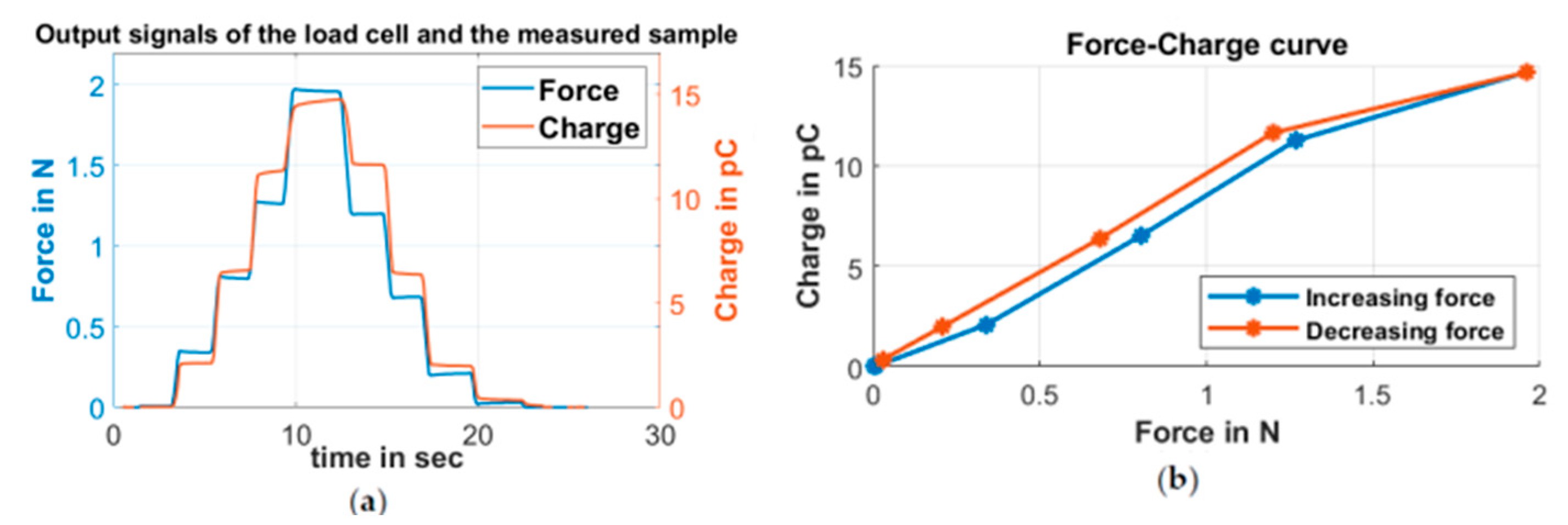
This work reports on the fabrication and testing of force sensors integrated directly into a printed circuit board (PCB). For this purpose, a layer of poly(vinylidene fluoride-trifluoroethylen) (P(VDF-TrFE)) is printed onto two pieces of two two-layer PCBs, which are then stacked together to create a four-layer PCB. The devised and fabricated sensor with the described measurement setup features a nearly linear measurement characteristic in the range between 0.3 and 1.2 N and a detection limit of approximately 10 mN.

1. Introduction

Poly(vinylidene fluoride) (PVDF) and its copolymers have been established as force-sensing materials in the recent years. They are commonly used in the form of foil [1], or are printed on metal surfaces and wafers [2]. These sensors are mostly discrete components, either soldered to printed circuit boards or connected via cables. The sensor concept presented here comprises integration directly into the printed circuit board (PCB), minimizing distances and facilitating even further system integration. This contribution describes the fabrication process, presents initial test data and discusses the possible drawbacks.

2. Materials and Methods

2.1. Fabrication

As a substrate, a two-layer printed circuit board (PCB) is designed with electrodes on each side and electrically conducting via connecting both sides. The PCB is commercially fabricated with additional “electroless nickel immersion gold” (ENIG) plating for minimal surface roughness. A layer of poly(vinylidene fluoride-trifluoroethylen) (P(VDF-TrFE)) is printed via stencil printing onto one side of the PCB featuring a thickness of approximately 17 µm. In order to create the stack shown in Figure 1a, two PCBs are placed on each other, bringing the P(VDF-TrFE) layers into direct contact.

2.2. Evaluation

To evaluate the sensor characteristics, i.e., sensitivity and the force–charge characteristic, a load cell (ALLURIS FMI250, Alluris, Freiburg im Breisgau, Germany) is pressed onto the sample using a motorized stage (Thorlabs MTS25, Thorlabs, Newton, NJ, USA) and 3D-printed brackets, as depicted in Figure 1c. The resulting charge signal of the sensor then is converted into a voltage signal using a charge meter (KISTLER Type 5015A, Kistler, Winterthur, Switzerland) and finally recorded using a multimeter (KEITHLEY DMM7510, Keithley, Cleveland, OH, USA). In order to reduce in-coupled noise due to long cable runs, the lowpass filter on the charge meter was set to a corner frequency 5 Hz. Electrical contact with the PCB sensor is achieved by using soldered copper strips.

2.3. Results

As seen in Figure 2a, the changes in force applied to the sensor can easily be detected in the charge output signal of the sensor. This result was achieved without additional filtering, signal processing or calibration. Figure 2b shows the nearly linear characteristics between 0.3 N and 1.2 N. At higher applied forces, a tendency to saturation becomes visible. In addition, a detection limit of approximately 10 mN has been observed in the entire measurement range.

3. Discussion

The results presented here demonstrate the possibility of integrating a printed P(VDF-TrFE) force sensor into a four-layer printed circuit board. The nonlinearities below 0.3 N and above 1.2 N could be mitigated using a more rigid test setup. In order to allow for a real integration, a method for creating a reliable bond between the P(VDF-TrFE) layers must be found, which is subject to ongoing research.

Author Contributions

Conceptualization, S.L.; methodology, S.L.; software, S.L.; validation, S.L. and W.H.; investigation, S.L.; writing—review and editing, all; visualization, S.L.; supervision, W.H.; project administration, W.H.; funding acquisition, B.J. All authors have read and agreed to the published version of the manuscript.

Funding

This research has been supported by the “LCM—K2 Center for Symbiotic Mechatronics”, within the framework of the Austrian COMET-K2 program.

Institutional Review Board Statement

Not applicable.

Informed Consent Statement

Not applicable.

Data Availability Statement

The data will be made available upon e-mail request.

Conflicts of Interest

The authors declare no conflicts of interest. There is no conflict of interest with E+E Elektronik GmbH.

References

  1. Schrüfer, E.; Reindl, L.; Zagar, B. Elektrische Messtechnik; Carl Hanser Verlag GmbH & Co. KG: Munich, Germany, 2018; pp. 1–13. ISBN 978-3-446-45654-9. [Google Scholar]
  2. Enser, H.; Sell, J.K.; Krause, M.; Schatzl-Linder, M.; Strauß, B.; Jakoby, B.; Hilber, W. Concept for Printed Ferroelectric Sensors on Coated Metallic Substrates. In Proceedings of the 2016 IEEE SENSORS, Orlando, FL, USA, 30 October–3 November 2016; pp. 1–3. [Google Scholar]
Figure 1. Evaluation and measurement setup: (a) cross-section of the PCB-P(VDF-TrFE) sensor design; (b) picture of a finished sample; (c) actual picture of the setup and the fabricated sensor stack.
Proceedings 97 00084 g001
Figure 2. Measurement data using an early sample: (a) sensor signal and force applied on the sensor during one measurement; (b) force-charge curve created using the data shown in (a) (averaged steps).
Proceedings 97 00084 g002
Disclaimer/Publisher’s Note: The statements, opinions and data contained in all publications are solely those of the individual author(s) and contributor(s) and not of MDPI and/or the editor(s). MDPI and/or the editor(s) disclaim responsibility for any injury to people or property resulting from any ideas, methods, instructions or products referred to in the content.