Proceeding Paper

Ultra-Resonance Microwave Defectoscopy of Metal Surfaces †

by
Oleksandr Malyuskin
Queen’s University Belfast, ECIT, Centre for Wireless Innovation, Belfast BT3 9DT, UK
Presented at the 6th International Electronic Conference on Sensors and Applications, 15–30 November 2019; Available online: https://ecsa-6.sciforum.net/.
Proceedings 2020, 42(1), 22; https://doi.org/10.3390/ecsa-6-06551
Published: 14 November 2019

Abstract

:
A novel microwave high-resolution near-field non-destructive testing technique is proposed and experimentally evaluated in reflectometry imaging scenarios involving planar metal surfaces. Traditionally, microwave reflectometry does not provide high dynamic contrast between the defect and background material in the case of metal structures due to intrinsically high reflection magnitude from the metal surfaces masking defect a microwave signature. A high-Q resonant sensor based on the loaded aperture is designed to interact very strongly even with small defects on the metal surface providing very high two-dimensional spatial resolution of approximately one tenth of a wavelength, λ, at λ/20–λ/10 standoff distance. Experimental results demonstrate a defect-to-background contrast greater than 5 dB amplitude and 50° phase in raw microwave data. To further enhance the spatial resolution and defect contrast, a phase-modulated near field imaging technique is proposed and experimentally evaluated in the case of a defected metal plate. This technique is based on fast variation of the reflection phase in the narrow frequency band around the resonance, which essentially enables elimination of background a microwave signature from the reflected signal. The proposed imaging technique should find applications in non-destructive surface testing and evaluation of metal and alloy structures.

Published: 14 November 2019

1. Introduction

Microwave reflectometry is a very useful tool in defect finding in many industrial and engineering applications [1]. It is used in different scenarios in non-destructive testing and imaging, for example, detection of faults in constructions [2] and composite materials [3], non-destructive testing of building structural integrity [4], biomaterials imaging [5], etc.
As an essential part of imaging setup, microwave probes (antennas) are used for microwave signal generation and collection of microwave response signal [1], Ref. [6] scattered off the sample under test. As the probe scans the imaging scene, the reflected signal changes as defined by the scattering properties of the sample under test, resulting in a raw microwave image. This image can be further processed, and features of interest (e.g., defects) can be extracted using various signal processing algorithms [7].
Traditionally used microwave probes are represented [1] by open ended waveguides, coaxial probes, dielectric resonator antennas and dielectric waveguides, small dipole antennas, etc. These probes operate reasonably well in the vicinity of the low-loss dielectrics or moderately lossy media, however, in general most of the existing probes fail to operate with high resolution and sensitivity in the proximity to metal, due to generation of out-of-phase electric currents on the metal surface that destructively interfere with the electric currents on the antenna surface. In the case of spatially extended aperture probes, such as open-ended waveguide, a very strong background reflection leads to extremely poor defect-to-background contrast, which limits the resolution and sensitivity.
Recently, a new class of loaded aperture probes [6] has been proposed. These probes’ operation is based on the generation of very strong resonant electric currents on the antenna inside the aperture. These probes were shown to enable very high spatial resolution and image contrast due to strong interaction with a defect in dielectric or moderately lossy media. In this work we extend the loaded aperture concept to create a deep subwavelength resonator probe whose resonance quality is not significantly affected by the proximity of metal surface. Yet, the sensor is highly sensitive to defects on the metal surface due to the resonance frequency shift introduced by the defects. We also demonstrate that the raw image resolution can be further improved by the application of a simple technique based on combining the raw images obtained at close frequencies in the vicinity of resonance. Advantages and limitations of the proposed technique are discussed on the basis of experimental results.

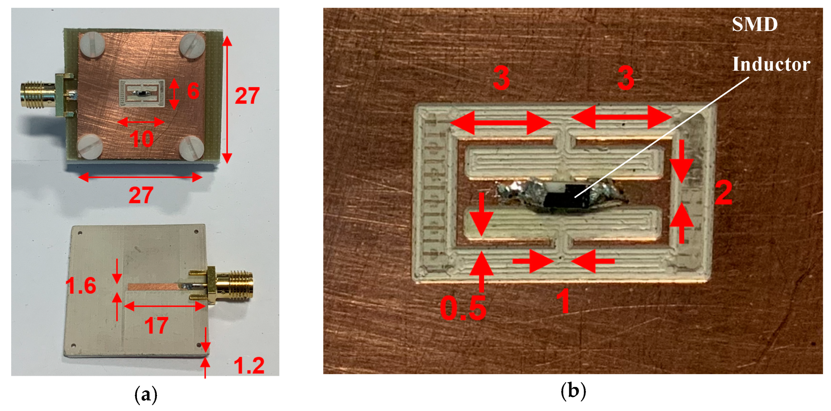
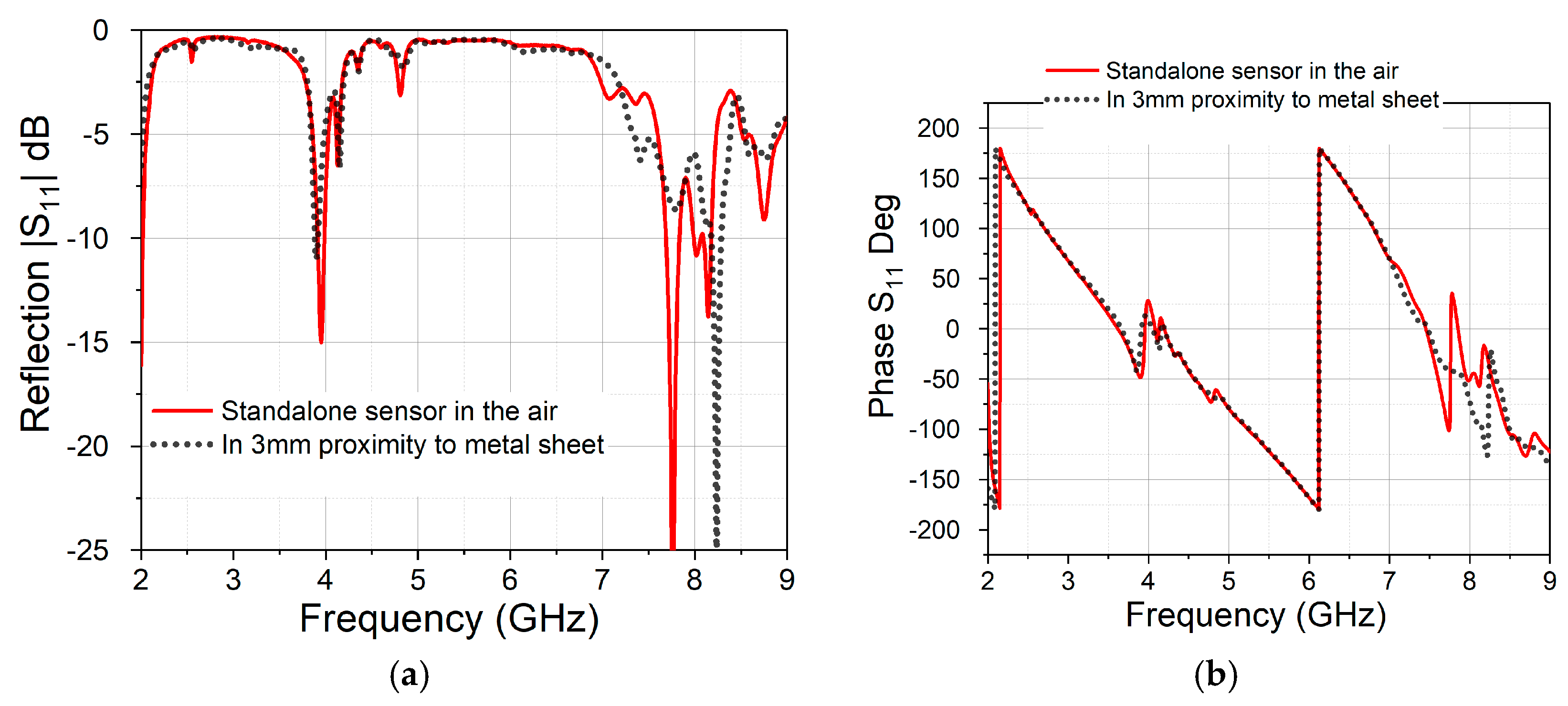
2. Microwave Resonance Sensor and Its Measured Reflection Parameter Characteristics

The fabricated sensor and its measured reflection parameter characteristics are shown in Figure 1 and Figure 2 respectively.
There are multiple resonances of the reflection parameter S11 at 2 GHz, 4 GHz, and 8 GHz for the sensor in 5 mm proximity to the metal sheet, Figure 2. Importantly, the resonance quality factor is practically not affected by the metal sheet proximity for all these resonances. However, proximity of the metal plate leads to the S11 resonance frequency shift, which can be used for high-resolution reflectometry imaging since defects on the metal surface will inevitably introduce an S11 frequency shift defined by their scattering characteristics. From the electromagnetic point of view, the resonance characteristics of the reflection parameter are defined by the re-distribution of the electric current inside of the loaded aperture resonator, destructive out-of-phase current interference is less significant in this case than in the imaging scenario involving conventional dipole or monopole microwave probes. Another important feature that is present in Figure 2b is large reflection phase variation in the narrow frequency band around the resonance. By combining reflected signals at close frequencies, it is possible to enhance features of the interest in the raw microwave image.

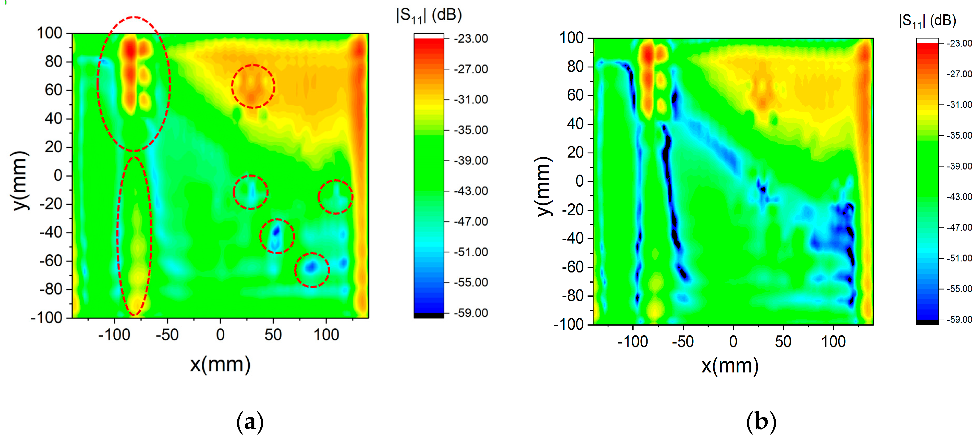
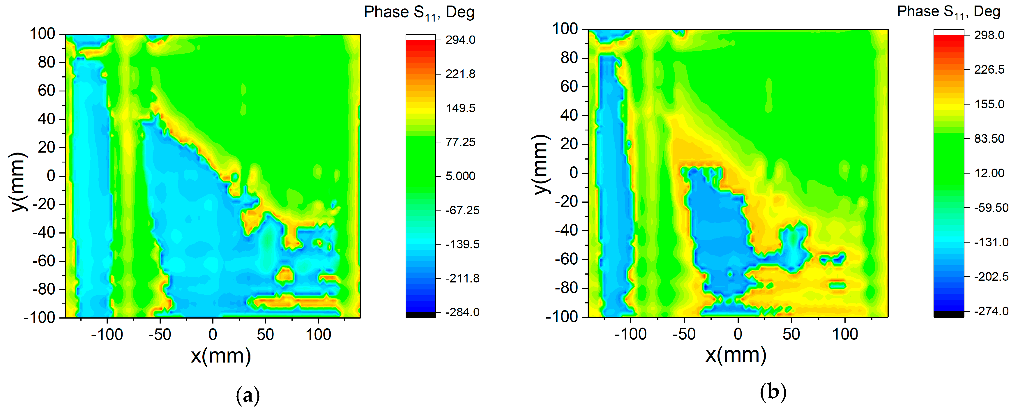
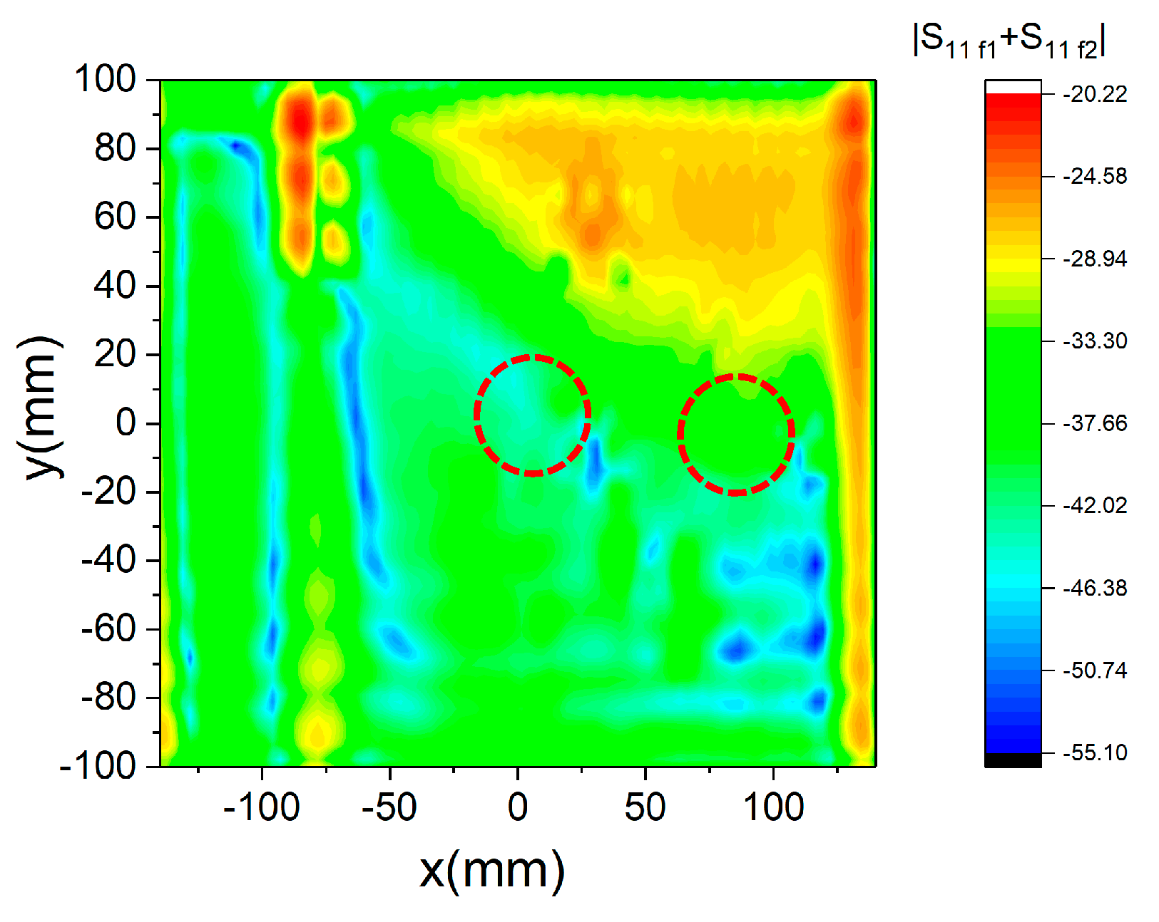
3. Experimental Reflectometry Results and Discussion

In this section we discuss the imaging setup, raw measured image characteristics, and “phase-modulated” raw image processing to increase defect resolution and possibly eliminate artefacts for the raw image.

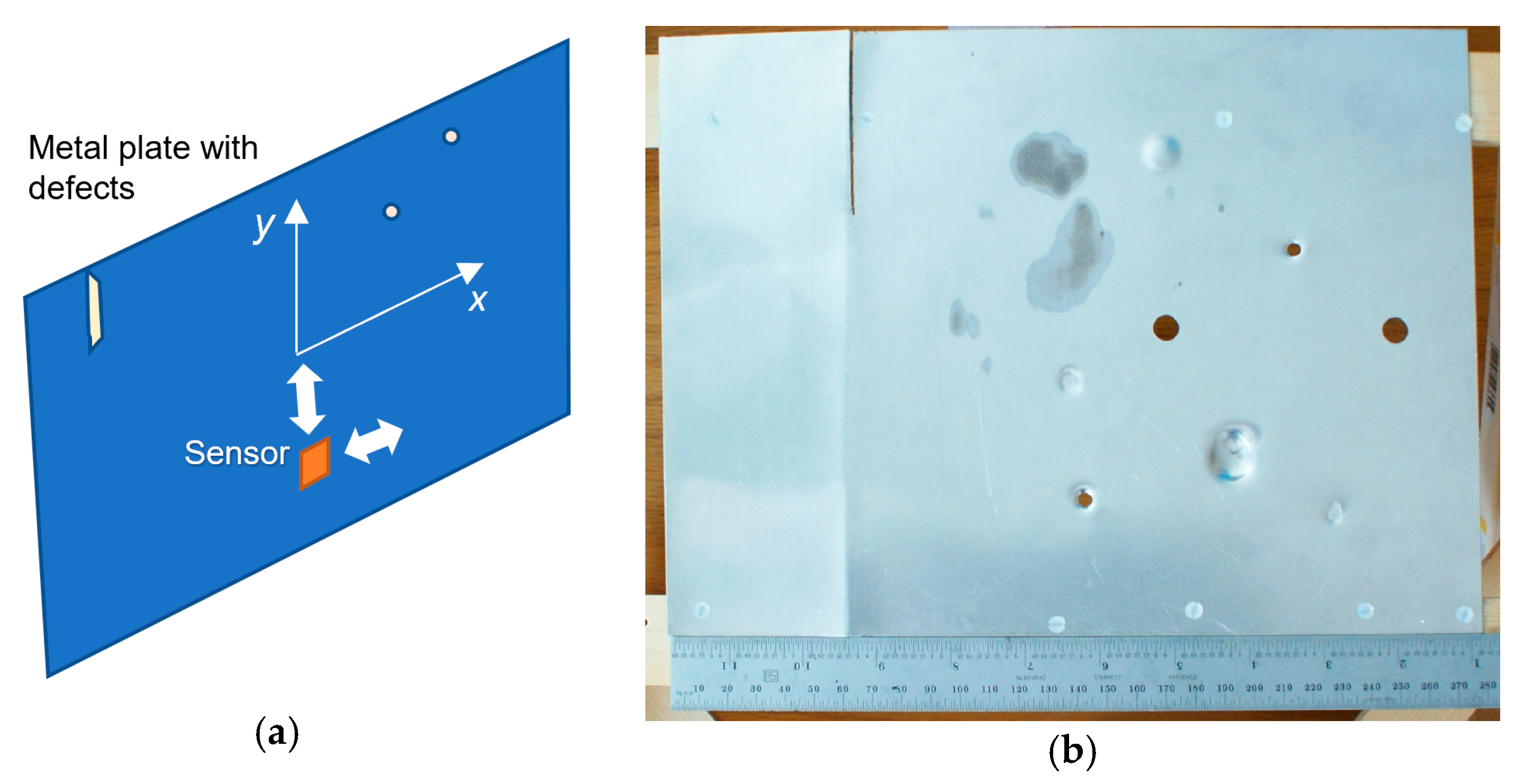
The Measurement Setup Geometry

The measurement setup geometry is shown schematically in Figure 3a. A microwave sensor is mounted on the positioner inside the near field anechoic environment. The positioner scans the defected metal plate in x and y ranges, and the signal is measured by the vector network analyzer for each spatial point and specified frequency range. The standoff distance of the sensor from metal plate in the z direction is 3 mm. In general, the standoff distance can vary in the 1 mm to 8 mm range (near-field evanescent zone). The defected metal plate is shown in Figure 3b.
From Figure 4a it can be seen that most of the defects are detected in the raw image with very high spatial resolution and contrast-to-background resolution of more than 5 dB (more than 10 dB in case of large defects like a slot in the top left corner). At the same time, for the raw microwave image at higher frequency, Figure 4b shows small defects much less clearly, but also introduces image artefacts that cannot be eliminated based on this image information only. Phase images of the S11 at the frequencies 7.7773 and 7.7776 GHz are shown in Figure 5 below.
It can be seen that for some imaging zones these images can be combined, to enhance or suppress the features of interest. This can be done by point-wise addition of the reflected signal real and imaginary parts,
|Scombined| = |S11 f1+ S11 f2|
where f1 and f2 are frequencies around the resonance. The result of this procedure is shown in Figure 6,
It can be seen that several artefacts present in the Figure 4b image are eliminated, namely two defects in the middle of the metal plate (encircled) are enhanced by around 4 dB. At the same time, some artefacts are still present, which requires iterative applications of the proposed algorithm at several frequencies. Another challenge is associated with very uneven surface of the defected board which complicates point-like defect localization. In this situation it might be worthwhile to reduce the Q-factor of the resonance sensor to achieve wider frequency bandwidth and better feature localization at the cost of defect-to-background contrast reduction.

Conflicts of Interest

The author declares no conflict of interest.

References

  1. Kharkovsky, S.; Zoughi, R. Microwave and millimeter wave nondestructive testing and evaluation—Overview and recent advances. IEEE Instrum. Meas. Mag. 2007, 10, 26–38. [Google Scholar] [CrossRef]
  2. Pauzi Ismail, M. Selection of suitable NDT methods for building inspection. IOP Conf. Ser. Mater. Sci. Eng. 2017, 271, 012085. [Google Scholar] [CrossRef]
  3. Zhang, H.; Yang, R.; He, Y.; Foudazi, A.; Cheng, L.; Tian, G. A Review of Microwave Thermography Nondestructive Testing and Evaluation. Sensors (Basel) 2017, 17, 1123. [Google Scholar] [CrossRef] [PubMed]
  4. Chung, K.L.; Zhang, C.; Li, Y.; Sun, L.; Ghannam, M. Microwave Non-Destructive Inspection and Prediction of Modulus of Rupture and Modulus of Elasticity of Engineered Cementitious Composites (ECCs) Using Dual-Frequency Correlation. Sensors (Basel) 2017, 17, 2831. [Google Scholar] [CrossRef] [PubMed]
  5. Malyuskin, O.; Fusco, V. Resonantly loaded apertures for high-resolution near-field surface imaging. IET Sci. Meas. Technol. 2015, 9, 783–791. [Google Scholar] [CrossRef]
  6. Malyuskin, O.; Fusco, V. High-Resolution Microwave Near-Field Surface Imaging Using Resonance Probes. IEEE Trans. Instrum. Meas. 2016, 36, 189–200. [Google Scholar] [CrossRef]
  7. Malyuskin, O.; Fusco, V. Super-Resolution Defect Characterization Using Microwave Near-Field Resonance Reflectometry and Cross-correlation Image Processing. Sens. Imaging 2017, 18, 7. [Google Scholar] [CrossRef]
Figure 1. (a) Geometry of an assembled sensor (top) and feeding microstrip layer (bottom). The relative permittivity of substrates is 10. There is no gap between the top layer and the feeding layer. Overall sensor thickness is 3.6 mm. The sensor’s standoff distance from the metal plate is 1 mm to 7 mm. (b) Enhanced view of the sensor aperture, where the sensor center-gap is loaded with a 3.6 nH surface-mount inductor. All dimensions are in mm.
Proceedings 42 00022 g001
Figure 2. Measured reflection parameter |S11|magnitude (a) and phase (b), of a standalone sensor in the air and in proximity to metal plate at stand-off distance of 5 mm.
Proceedings 42 00022 g002
Figure 3. (a) Schematic geometry of scanning near field setup. The sensor’s standoff distance from the metal plate is 1 mm to 7 mm. (b) Metal plate with various defects.
Proceedings 42 00022 g003
Figure 4. Reflected image represented by the |S11|parameter magnitude at different frequencies: (a) 7.7773 GHz. (b) 7.7776 GHz. Encircled areas on Figure 4a show actual defects.
Proceedings 42 00022 g004
Figure 5. Reflected image represented by the S11 parameter phase at different frequencies: (a) 7.7773 GHz. (b) 7.7776 GHz.
Proceedings 42 00022 g005
Figure 6. Combined S11 image represented at 7.7773 GHz and 7.7776 GHz.
Proceedings 42 00022 g006
Publisher’s Note: MDPI stays neutral with regard to jurisdictional claims in published maps and institutional affiliations.

