Proceeding Paper

Pore Morphology of Heavily Doped P-Type Porous Silicon †

by
David Martín-Sánchez
,
Salvador Ponce-Alcántara
and
Jaime García-Rupérez
*
Nanophotonics Technology Center (NTC), Universitat Politècnica de València, 46022 Valencia, Spain
*
Author to whom correspondence should be addressed.
Presented at the 5th International Electronic Conference on Sensors and Applications, 15–30 November 2018; Available online: https://ecsa-5.sciforum.net.
Proceedings 2019, 4(1), 14; https://doi.org/10.3390/ecsa-5-05715
Published: 14 November 2018
(This article belongs to the Proceedings of 5th International Electronic Conference on Sensors and Applications)

Abstract

:
Tuning the pore diameter of porous silicon (PS) is essential for some applications such as biosensing, where the pore size can filter the entrance of some analytes or increase its sensitivity. However, macropore (>50 nm) formation on p-type silicon is still poorly known due to the strong dependence on resistivity. Electrochemically etching heavily doped p-type silicon usually forms micropores (<5 nm), but it has been found that bigger sizes can be achieved by adding an organic solvent to the electrolyte. In this work, we present the results of using dimethylformamide (DMF), dimethylsulfoxide (DMSO), potassium hydroxide (KOH) and sodium hydroxide (NaOH) for macropore formation in p-type silicon with a resistivity between 0.001 and 0.02 Ω∙cm, achieving pore sizes from 5 to 100 nm.

1. Introduction

Porous silicon (PS) is a nanostructured material generated by electrochemically etching silicon (Si) into electrolytes containing hydrofluoric acid (HF) [1]. The growth of the pores is a combination of two chemical reactions: a direct dissolution of Si in fluoride and the oxidation of Si in the presence of oxygen and its later dissolution [2]. Both reactions are strongly dependent on etching conditions, both chemical and electrical [3].
PS has many potential application areas such as optoelectronics and biosensing [4,5,6], mainly because it retains the advantages of silicon technology while adding the ability of controlling optical properties. Porosity, thickness, pore diameter, pore morphology and distance between pores are some of the tunable properties available during fabrication [7]. High porosities combined with small pore diameters commonly lead to high sensitivity sensors. Contrarily, high pore diameters allow a better adsorption ability. On the other hand, when using PS membranes for sensing, longer distances between pores are preferred for a better endurance. Unfortunately, not all combinations of parameters are possible or at least different approximations must be carried out to overcome the initial limitations.
The macropore (pores with average diameter greater than 50 nm) formation mechanism on n-type silicon is well known [3,8]. Low-doped p-type silicon wafers have also been used for macropore formation [9]. However, achieving mesopores (5–50 nm) and macropores in moderately-doped and heavily-doped silicon is more challenging. Aqueous HF-based electrolytes (HF diluted in water and optionally surfactants such as alcohols) will yield only micropores (<5 nm) and mesopores if no additional fabrication step is introduced [10,11]. In order to overtake this limitation, several approaches have been developed:
  • PS oxidation and HF dissolution. When PS is thermally oxidized, a SiO2 layer is formed on its surface. Dissolution of this oxide in HF can increase the pore diameter up to half the SiO2 layer thickness [12]. This process can be repeated but doing so will reduce the pore walls and jeopardize the structural stability.
  • Post-treatment with alkaline mixtures. KOH and NaOH solutions anisotropically etch Si and can be used to expand the pores after fabrication [13], although this method has the same limitations as the previous one. They have also been used for partially dissolving the PS film and obtaining a pattern that—if used afterwards in a new electrochemical etching—can yield macropores [6].
  • Organic electrolytes. The combination of HF-based solutions with non-aqueous electrolytes, e.g., dimethylformamide and dimethylsulfoxide, facilitates the Si dissolution during anodization [14,15]. This method offers more control over the PS properties.
Even though numerous studies have reported the obtainment of macropores on heavily-doped p-type silicon, there is still a lack of analyses for certain ranges of resistivity.

2. Methods

PS was prepared by electrochemically etching p-type silicon wafers (boron doped, <100> oriented) with different resistivity: 0.001–0.005 Ω∙cm and 0.01–0.02 Ω∙cm, both purchased from MicroChemicals GmbH (Ulm, Germany). Aqueous electrolytes were prepared with ethanol (EtOH) obtained from Scharlab S.L. (Barcelona, Spain) and hydrofluoric acid (HF) (48% solution in water) purchased from BASF (Ludwigshafen am Rhein, Germany). For organic electrolytes, N,N-dimethylformamide (DMF) from Sigma-Aldrich (Saint Louis, MO, USA) and dimethylsulfoxide (DMSO) from Scharlab S.L. (Spain) were employed. In the cases where alkaline solutions were used, potassium hydroxide (KOH), obtained from Panreac S.L. (Barcelona, Spain), and sodium hydroxide (NaOH), from Scharlab S.L. (Spain), were mixed in different concentrations with deionized water (DIW) produced in house by a Millipore water purification system.
For cleaning purposes, all samples were pretreated for 30 min in a 3:1 volumetric mixture of sulfuric acid (H2SO4) and hydrogen peroxide (H2O2), both purchased from BASF (Germany), for removing organic residues off the substrate. Afterwards, they were dipped into a solution of <5% HF for 30 s in order to eliminate the native oxide layer.
Electrochemical etching of Si was performed under galvanostatic conditions in a vertical cell in which a Pt electrode worked as a cathode and the Si itself as anode. Different aqueous and organic solutions have been used as electrolytes.
Field emission scanning electron microscopy (FESEM) was performed using both a Hitachi S-4500 SEM and a Zeiss Ultra 55 microscope.

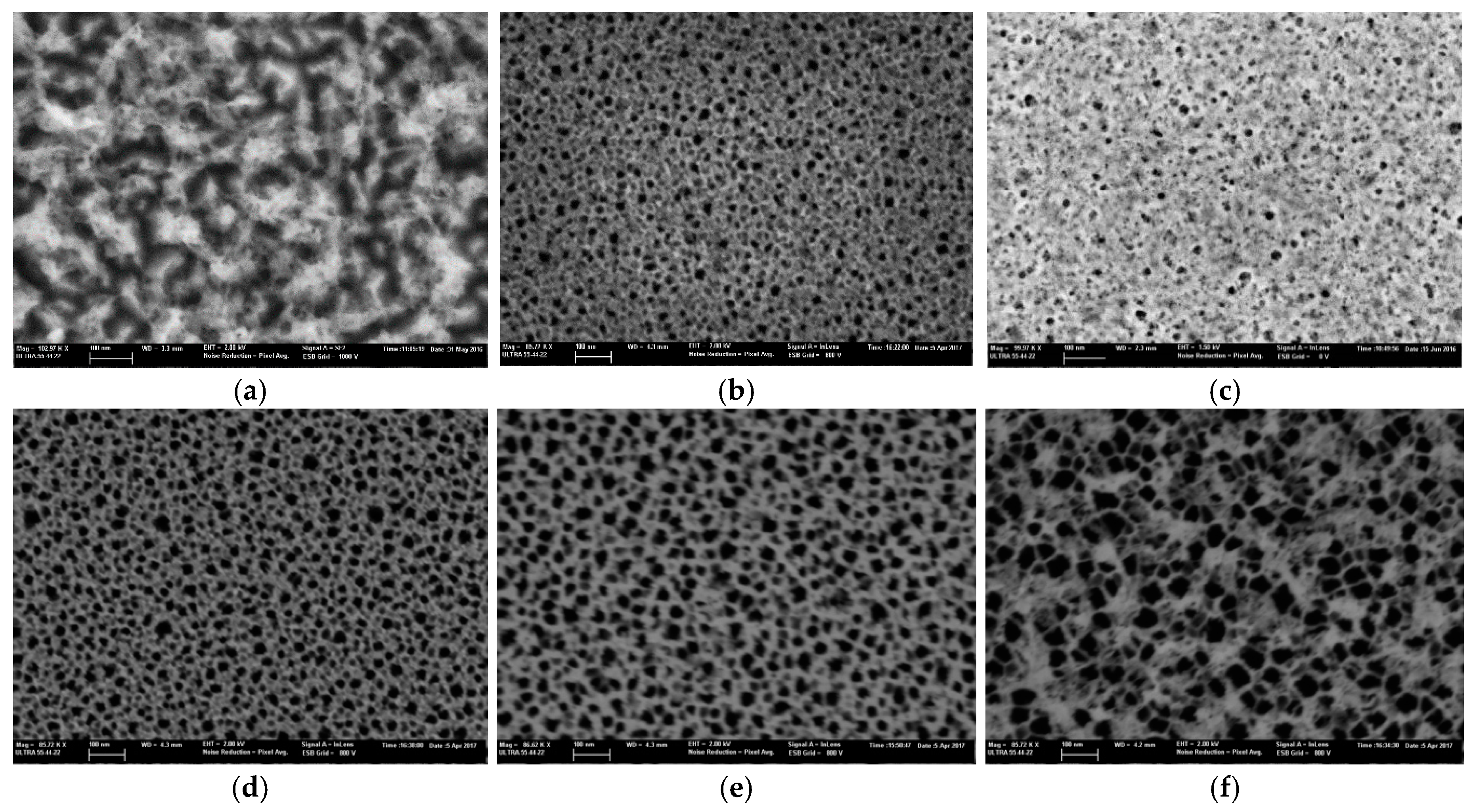
3. Results and Discussion

The results of the pore morphology dependence with different etching parameters for a resistivity of 0.01–0.02 Ω∙cm are summarized in Table 1.
The lower the HF concentration within the electrolyte, the bigger the pore would be. However, etching heavily doped silicon wafers with very low HF concentrations (Figure 1a) lead to pore interconnection. This implied thin walls and a slow vertical growth. PS films created this way would be structurally weak and only a small range of porosities can be achieved. Rising the HF concentration reduced the pore diameter but strengthened the structure. PS films formed this way were not appropriate to be used as membranes but they may be suitable for sensing gas or humidity, due to its high sensitivity.
Comparing Figure 1b,c, we can see that both samples have similar pore diameters. The difference between those two images is pore interspacing, being higher in the case of the KOH etching of the PS film. This effect was caused due to the deposition of the Si on the surface and could be reduced if agitation is added.
Adding DMF to the electrolyte yielded higher pore diameters. It can be seen in Figure 1d,e that increasing DMF proportion directly increased the pore size. These PS samples are more convenient than the ones etched with aqueous electrolytes for applications such as biodetection since the pore size allows the entrance of molecules and proteins. Instead, anodization with DMSO resulted in pores extremely close to adjacent pores, creating a hive-like structure (see Figure 1f) and adopting a hexagonal form instead of the typical circular one. PS films formed with 1:1:9 DMF and DMSO were structurally more fragile than the other electrolytes, and also organic electrolytes had a negative impact on vertical uniformity but pore diameters up to 50 nm could be achieved.
In Table 2, the results for a resistivity of 0.001–0.005 Ω∙cm are shown. Oxidation of PS films and removal dipping in HF as well as alkaline etching were omitted as they yielded intermediate pore sizes.
In this case, for some HF concentrations, a small layer of micropores appeared on top of the desired layer. It could be easily removed by dipping the sample in a 1 M NaOH dissolution in order to achieve PS films with pore diameters up to 100 nm (see Figure 2). These sensors display lower sensitivities but are preferred in some applications for its adsorption ability.

4. Conclusions

Pore morphology and fabrication properties for PS formed in heavily doped p-type Si (100) have been presented. The effect of organic electrolytes such as DMF and DMSO and alkaline etchants e.g., KOH and NaOH has been reported. The use of organic electrolytes on Si wafers with a resistivity of 0.01–0.02 Ω∙cm showed an increase the pore diameter of up to 50 nm. On the other hand, pore sizes of around 100 nm could be achieved on wafers with a lower resistivity. Macropores could be formed in heavily doped p-type Si, which could allow for a wider range in the design of PS based sensors for different applications.

Acknowledgments

The authors acknowledge funding from the Spanish government through the project TEC2015-63838-C3-1-R-OPTONANOSENS.

References

  1. Pacholski, C. Photonic crystal sensors based on porous silicon. Sensors 2013, 13, 4697–4713. [Google Scholar] [CrossRef] [PubMed]
  2. Föll, H.; Christophersen, M.; Carstensen, J.; Hasse, G. Formation and application of porous silicon. Mater. Sci. Eng. R. 2002, 39, 93–141. [Google Scholar] [CrossRef]
  3. Zhang, G.X. Porous silicon: Morphology and formation mechanisms. In Modern Aspects of Electrochemistry; Vayenas, C., Gamboa-Adelco, M.E., Eds.; Springer: Boston, MA, USA, 2006; Volume 39, pp. 65–133. ISBN 0076-9924. [Google Scholar]
  4. Caroselli, R.; Ponce-Alcántara, S.; Prats-Quílez, F.; Martín-Sánchez, D.; Torrijos-Morán, L.; Griol-Barres, A.; Bellieres, L.; Bandarenka, H.; Girel, K.; Bondarenko, V.; et al. Experimental study of the sensitivity of a porous silicon ring resonator sensor using continuous in-flow measurements. Opt. Express 2017, 25, 31651–31659. [Google Scholar] [CrossRef] [PubMed]
  5. Hutter, T.; Horesh, M.; Ruschin, S. Method for increasing reliability in gas detection based on indicator gradient in a sensor array. Sens. Actuators B 2011, 152, 29–36. [Google Scholar] [CrossRef]
  6. Mariani, S.; Strambini, L.M.; Barillaro, G. Femtomole detection of proteins using a label-free nanostructured porous silicon interferometer for perspective ultrasensitive biosensing. Anal. Chem. 2016, 88, 8502–8509. [Google Scholar] [CrossRef] [PubMed]
  7. Canham, L.T. Tunable properties of porous silicon. In Handbook of Porous Silicon; Canham, L.T., Ed.; Springer International Publishing: Geneva, Switzerland, 2014; pp. 201–206. ISBN 978-3-319-05744-6. [Google Scholar]
  8. Lehman, V.; Föll, H. Formation mechanism and properties of electrochemically etched trenches in n-type silicon. J. Electrochem. Soc. 1990, 137, 653–659. [Google Scholar] [CrossRef]
  9. Lehman, V.; Rönnebeck, S. The physics of macropore formation in low-doped p-type silicon. J. Electrochem. Soc. 1999, 146, 2968–2975. [Google Scholar] [CrossRef]
  10. Lehman, V.; Stengl, R.; Luigart, A. On the morphology and the electrochemical formation mechanism of mesoporous silicon. Mater. Sci. Eng. B 2000, 69–70, 11–22. [Google Scholar] [CrossRef]
  11. Mariani, S.; Pino, L.; Strambini, L.M.; Tedeschi, L.; Barillaro, G. 10000-fold improvement in protein detection using nanostructured porous silicon interferometric aptasensors. ACS Sens. 2016, 1, 1471–1479. [Google Scholar] [CrossRef]
  12. Lau, H.W.; Parker, G.J.; Greef, R. High-aspect ratio silicon pillars fabricated by electrochemical etching and oxidation of macroporous silicon. Thin Solid Films 1996, 276, 29–31. [Google Scholar] [CrossRef]
  13. Chernienko, A.V.; Astrova, E.V.; Zharova, Y.A. Zigzag structures obtained by anisotropic etching of macroporous silicon. Tech. Phys. Lett. 2013, 39, 990–993. [Google Scholar] [CrossRef]
  14. Ponomarev, E.A.; Lévy-Clément, C. Macropore formation on p-type silicon. J. Porous Mater. 2000, 7, 51–56. [Google Scholar] [CrossRef]
  15. Haldar, S.; De, A.; Chakraborty, S.; Ghosh, S.; Ghanta, U. Effect of dimethylformamide, current density and resistivity on pore geometry in p-type macroporous silicon. Procedia Mater. Sci. 2014, 5, 764–771. [Google Scholar] [CrossRef]
Figure 1. Field emission scanning electron microscopy (FESEM) images of electrochemically etched p-type Si 0.01–0.02 Ω∙cm (a) hydrofluoric acid (HF):ethanol (EtOH) 1:9, I = 22 mA/cm2, T = 90 s, (b) HF:EtOH 1:2, I = 6 mA/cm2, T = 100 s, oxidized for 30 min and dipped in HF, (c) HF:EtOH 1:2, I = 6 mA/cm2, T = 120 s, etched with 45 mg of potassium hydroxide (KOH) in 100 mL of deionized water (DIW) for 5 min, (d) HF:DIW:N,N-dimethylformamide (DMF) 1:1:4, I = 22 mA/cm2, T = 90 s (e) HF:DIW:DMF 1:1:9, I = 11 mA/cm2, T = 90 s and (f) HF:DIW:dimethylsulfoxide (DMSO) 1:1:9, I = 11 mA/cm2, T = 90 s.
Proceedings 04 00014 g001
Figure 2. FESEM images of electrochemically etched p-type Si 0.001–0.005 Ω∙cm (a) HF:EtOH 2:1, I = 650 mA/cm2, T = 30 s, (b) HF:EtOH 2:1, I = 730 mA/cm2, T = 30 s, dissolved 2 min in 0.1 M NaOH.
Proceedings 04 00014 g002
Table 1. Influence on pore morphology of fabrication parameters for a resistivity of 0.01–0.02 Ω∙cm.
ElectrolyteHF:EtOH 1:9HF:EtOH 1:2 + OxidationHF:EtOH 1:2 + KOHHF:DIW:DMF 1:1:4HF:DIW:DMF 1:1:9HF:DIW:DMSO 1:1:9
Resistivity of the electrolyte150 Ω∙cm100 Ω∙cm100 Ω∙cm750 Ω∙cm1300 Ω∙cm1500 Ω∙cm
Current range of PS formation<18 mA/cm2<130 mA/cm2<130 mA/cm2<25 mA/cm2<18 mA/cm2<18 mA/cm2
Pore surface shapePores inter-connectedHolesHolesHolesHolesHexagons
Pore section shapeRandom and short branchesSecondary branches onlySecondary branches onlySecondary branches onlySecondary branches onlySmooth pore wall
Pore diameter~20 nm~25 nm~25 nm~25 nm~30 nm~50 nm
Etch rate~0.5 nm/s,
I = 5 mA/cm2,
T = 310 s
~8 nm/s,
I = 6 mA/cm2,
T = 100 s
~8 nm/s,
I = 6 mA/cm2,
T = 120 s
~20 nm/s,
I = 22 mA/cm2,
T = 90 s
~8 nm/s,
I = 11 mA/cm2,
T = 90 s
~5 nm/s,
I = 11 mA/cm2,
T = 90 s
Spacing between pores~50 nm~30 nm~60 nm~40 nm~20 nm<10 nm
Micropore layer on topNoNoNoNoNoNo
Table 2. Influence on pore morphology of fabrication parameters for a resistivity of 0.001–0.005 Ω∙cm.
ElectrolyteHF:EtOH 2:1HF:EtOH 2:1 + NaOH
Resistivity of the electrolyte10 Ω∙cm10 Ω∙cm
Current range of PS formation<750 mA/cm2<750 mA/cm2
Pore surface shapeHolesHoles
Pore section shapeSecondary branches onlySecondary branches only
Pore diameter<10 nm~100 nm
Etch rate~400 nm/s, I = 650 mA/cm2, T = 30 s~450 nm/s, I = 730 mA/cm2, T = 30 s
Spacing between pores~20 nm~20 nm
Micropore layer on topYesNo

