1. Introduction
Fabricating of thin and ultrathin films as well as periodic layers by liquid phase epitaxy (LPE) is a complicated problem from the viewpoint of homogeneity of the layers obtained as well as their reproducibility. All the variants of LPE have similar factors affecting the quality, size and composition of the layers being deposited. Namely:
In the work [
5] the authors have formulated basic requirements to the new LPE technique. Its implementation will make it possible to obtain more perfect thin and ultrathin films as well as periodic layers.
Based the analysis of the work [
5] we proposed the new technique of liquid phase epitaxy—scanning liquid phase epitaxy [
6].
2. Scanning Liquid Phase Epitaxy
2.1. The Technique Description
Operating principles of the technique are as follows. A solution-melt in the homogenization container (vessel) at the homogenization temperature is brought into contact with a cooled substrate for a short period of time. After growing of just a part of the layer or the whole one, the substrate is cleansed immediately of the solution-melt, which is returned to the homogenization container. The special feature of the process is that the wetting of the substrate and/or its cleansing of the solution-melt is realized by using Ampere force which acts on the solution-melt as the electric current and the magnetic field pass through it in certain directions [
7].
The other feature of the LPE technique developed is that the substrate and the solution-melt are contacted pointwise (or segmentally) over the substrate surface by means of mechanical scanning device. Here the moving part could be either the substrate or the growing vessel.
2.2. The Apparatus Description
The apparatus for realization of the technique proposed represents the gas camera where the growing vessel is placed. The growing vessel control unit may be located separately and could be connected with the growing vessel through the interface at the one of gas camera panels.
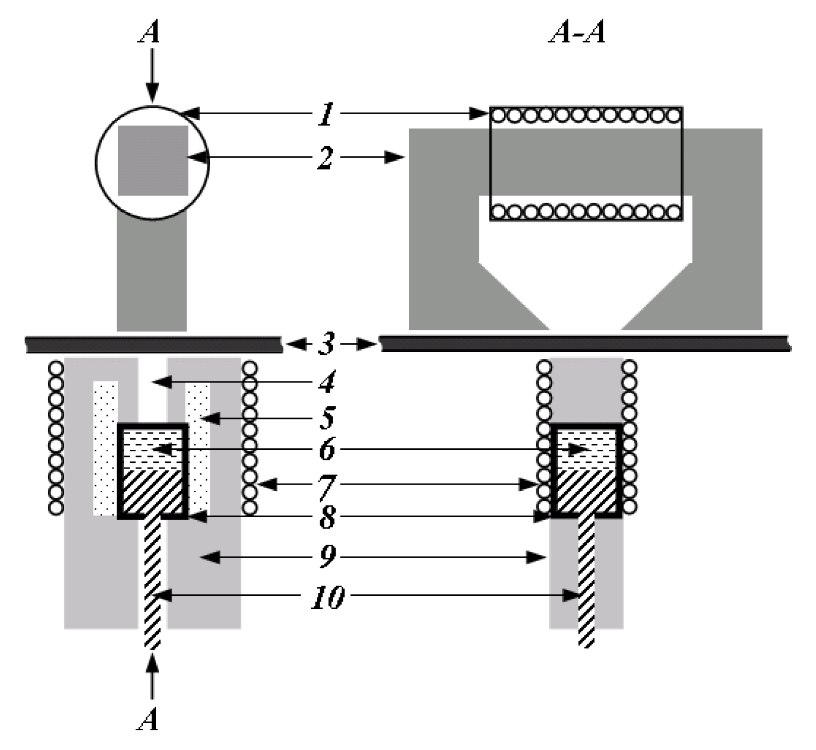
Figure 1 shows the growing vessel allowing to realize the new technique.
The growing vessel could be also realized differently. For example, magnetic conductor could be located under the substrate or both the solution-melt and the magnetic conductor may be located over the substrate. If the Ampere force and its direction are controlled only by the magnitude and the direction of the current, then it is possible to use permanent magnets for creation of the magnetic field. Thus, a versatility of the technique proposed is provided due to utilization of various combinations of the construction elements.
The growing vessel proposed is equipped with specially configured electrodes as shown in
Figure 1. It allows to create current and magnetic field gradients in the solution-melt: maximum current and maximum magnetic field are at the growth interface. Thus Ampere force acting on the solution-melt is maximal at the interface between the substrate and the solution-melt as well. In turn, the value of current and the magnetic field magnitude are chosen to provide the Ampere force exceeding over adhesive force between the solution-melt and the substrate taking into account the solution-melt gravity force. It is important that the heating assembly heats only the solution-melt and partially the electrodes. This makes the heating processes to be much less inert.
It is important that in the design presented the homogenization container and the growth capillary are separate elements. This allows to remove an oxide film from the solution-melt surface after the homogenization stage during moving the solution-melt into the growth capillary. Since the heater is small-sized and is located on the growing vessel there are no special temperature requirements to the gas camera material. Thus it could be manufactured using available low-temperature materials. Basic requirement to the gas camera is that it should have enough room for the growing vessel and for the substrate of a desired area.
2.3. The Technique of Epitaxial Layers Growing
Every act of growing of either a part of epitaxial layer or entire layer (over the whole area or just a portion of substrate surface) consists of five stages:
Stage 1. Wetting the substrate by the solution-melt. The solution-melt is in the homogenization container at the homogenization temperature. The substrate has a lower temperature. The solution-melt is moved from the homogenization container into the growth capillary with the help of the piston—
Figure 1. A current is supplied to the solution-melt simultaneously with the magnetic field in the direction providing Ampere force to be guided towards the interface between the solution-melt and the substrate.
Stage 2. Growing of a part of the epitaxial layer or the entire layer. During the contact between the solution-melt and the cooled substrate the deposition of the epitaxial layer of a certain thickness occurs after the time period chosen. The thickness of the layer grown at the given temperature could be controlled by the contact time between the solution-melt and the cooled substrate and/or by the value of the substrate cooling.
Stage 3. Removing the solution-melt from the substrate. It is realized by instantaneous changing of the direction of Ampere force acting on the solution-melt. For example, it is possible to change instantly the direction of the current through the solution-melt. The magnitude of Ampere force is calculated so as to exceed the adhesion/cohesion force and taking into account the gravity force acting on the solution-melt.
Stage 4. The solution-melt return into the homogenization container. This could be achieved by various ways depending on the growing vessel configuration chosen. For example, for the growing vessel design proposed (see
Figure 1) the solution-melt is returned back to the homogenization container under the gravity force and/or Ampere force (the piston must be at the lowest position).
Stage 5. Homogenization of the solution-melt in the homogenization container. It is realized at a homogenization temperature during certain calculated amount of time.
3. Results and Discussion
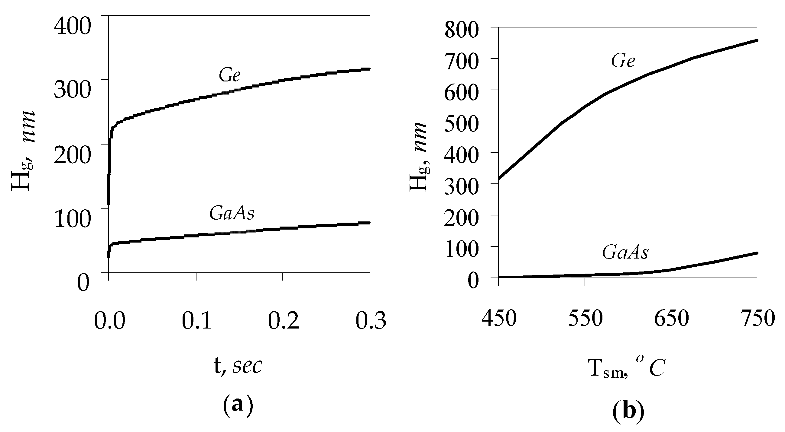
The results of the modeling of heat and mass transfer processes in the growing vessel for scanning LPE developed are shown in
Figure 2.
As it can be seen from the graphs in
Figure 2 there is a principal possibility of obtaining of thin and ultrathin layers by the technique developed.
We manufactured the pilot apparatus for scanning LPE. Functionality of the mechanisms of substrate wetting and cleaning of a solution-melt by the Ampere force is established. Preliminary experimental investigations of the systems GaAs/GaAs and Ge/GaAs (Ga solution-melts) showed the principal possibility of growing the epitaxial layer by this technique.
In comparison with known LPE technique variants [
8], scanning LPE provides the duration of a short-time contact between the solution-melt and the substrate less than a second. According to our calculations such a short time value makes it possible to reduce the thickness of uncontrollably grown epitaxial layer by more than the order of magnitude as the temperature instability of the heating assembly is eliminated, and to avoid the formation of convective streams.
In contrast to known pulse variants of LPE [
9,
10], in the proposed technique the heating assembly heats the solution-melt directly while the substrate is located at the independent temperature zone. Owing to this, the heating and cooling time of the substrate is shortened from tens of minutes up to few seconds. Both the short-time contact between the solution-melt and the substrate as well as the low heat process inertia allow to reduce by one order and more the depth of diffusion of the solution-melt components and the components of epitaxial layers grown further into the bulk of substrate. In addition, segmental epitaxial layers grown on the substrate surface do not require continuous heating as it takes place in other LPE variants. This affects the diffusion depth as well if there remains a thin layer of a solution-melt on the substrate after the growth process.
The substrate cleaning of the solution-melt is more rapid and more controllable in comparison with other methods due to the electrical process used for Ampere force creation. Also it is possible to cleanse the substrate of the solution-melt totally depending on the wetting angle between the solution-melt and the substrate.
Initial substrate overcooling before the contact with the solution-melt allows to avoid uncontrolled phase equilibrium shift and to create the conditions of instantaneous crystallization of the epitaxial layer, i.e., without dissolving of previously grown layers. In addition, when the solution-melt returns to the homogenization container after every growth act there is no solution-melt depletion by the components being deposited.
Segmental growth of continuous epitaxial layer over the substrate surface makes it possible to use very large area substrates.
4. Conclusions
The new technique of liquid phase epitaxy—scanning LPE allowing to realize short-time contact between a solution-melt and a substrate was developed. The principal possibility of thin and ultrathin layers obtaining was shown.


