Abstract
By laser micromilling technology it is possible to fabricate custom MEMS microhotplate platform and also SMD package for MOX sensor, that gives complete solution for integration in mobile devices-smart phones, tablets and etc. The 3D design and fabrication of MEMS microhotplates and packages products occurs simultaneously that give opportunity for ultra-fast time making unique solutions for MOX sensors (number of microhotplates, hot spot size on microhotplates, diameter holes in package cap and etc.) without looking at standard solutions (primarily the package type).
Published: 19 June 2019
1. Introduction
The main idea of our developed technological flow based on laser micromilling is wide flexibility in developing of MEMS and SMD structures. Using of equipments only widely presented on the market and refusing of technological steps needs a clean rooms support. Only semi custom 3D printing type software is especially developed product for laser micromilling system needed for successful development and production of MEMS and SMD structure during our experiments. Software is needed for translation CNC code to 4-axis laser micromilling setup and online measuring of geometrical parameters of MEMS and SMD structure for corrections micromilling procedure during automatic production.
2. Experimental
During our work, an Ytterbium pulsing 20 W fiber laser with a wavelength of 1.064 μm and tunable pulse duration from 50 to 200 ns is used. This laser emitter is installed on the four-coordinate portal complex, which allows the laser scanner to be moved across wilde field. The processing of ceramic substrates is carried out in a snap-in fixed in a rotational device, which allows processing of flat substrates on both sides, cylindrical substrates over the entire surface area. Currently, fiber markers are most often used in industry for marking various types of products and are not intended for 3D laser milling, despite the fact that the technical capabilities of any laser marker allow it by using of our developed software. Fabrication of MOX sensors includes the following main steps:
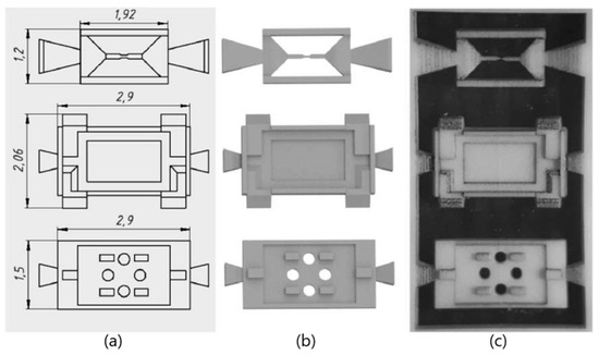
- MEMS microhotplate modeling and both bottom and top parts of the SMD package (Figure 1) in 3D CAD programs with output file in STL format and also 2D modeling of MEMS and SMD metallization topology in DXF format;
 Figure 1. (a) Sketch with dimension in mm for parts of MEMS microhotplate (on top) and SOT-23 package (in bottom); (b) 3D model of sketch as screenshot in CAD program; (c) Parts of MEMS and SMD package after laser micromilling by using 3D models of MEMS.
 - Optionally MEMS microhotplate parameters could be simulated in COMSOL program, which allows to predict approximate thermal characteristics of the MOX sensor;
- 4-axis laser facility is used for monolithic ceramics laser micromilling with help of 3D models of bottom and top parts of the SMD package and MEMS microhotplate;
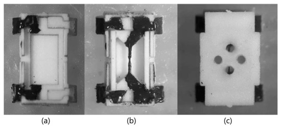
- Platinum metallization deposition according with 2D model of topology, metallization annealing paying attention to specification on jet or screen-print platinum materials (Figure 2);
 Figure 2. (a) Deposited Pt paste on bottom part of SOT-23 package; (b) Deposited Pt paste on MEMS part inside SOT-23 package; (c) The assembled SOT-23 package before firing.
 - Optionally the metallization can be processed with laser according with 2D model;
- MOX gas sensitive layer deposition and annealing on the MEMS microhotplate;
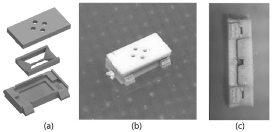
- Assembling separate parts of sensor into one SMD package and adhesion with special glass (Figure 3)
 Figure 3. (a) 3D model assembling of SOT-23 package; (b) The top view of SOT-23 assembled package; (c) The side view SOT-23 assembled package.
Using described tech flow, experiments were carried out to fabricate a possible minimum size of MEMS microhotplate from Al2O3 ceramics. The minimum size of the manufactured microhotplate with 250 mW power consumption at 450 °C with track width was 30 μm and 20 μm thickness in SMD SOT-23 package type (3.0 × 1.4 × 1.0 mm with max dissipating power at 20 °C–350 mW) were achieved. Tests of fabricated MEMS microhotplate present in work [1].
Advantage of ceramic using as a material for laser micromilling is extension of MOX sensor working temperatures range up to 1000 °C compare with typical 700 °C for silicon technology. Also useful advantage of fully ceramics based MOX sensor is long term stability against harsh environmental conditions including extreme temperature and acid or alkaline gases.
This research was funded by Ministry of Science and Higher Education of Russian Federation under grant number 14.584.21.0054 from 26 November 2018, unique identifier RFMEFI58718X0054.
Reference
- Samotaev, N.; Oblov, K.; Ivanova, A. Laser micromilling technology as a key for rapid prototyping SMD ceramic MEMS devices. In Proceedings of the MATEC Web of Conferences, Jeju Island, South Korea, 19–20 July 2018. [Google Scholar]
© 2019 by the authors. Licensee MDPI, Basel, Switzerland. This article is an open access article distributed under the terms and conditions of the Creative Commons Attribution (CC BY) license (https://creativecommons.org/licenses/by/4.0/).