Extended Abstract

H2S Sensing Properties of a Diode-Type Device Using ZnO Nanorods Coupled with CuO Nanocrystals †

1
Faculty of Advanced Science and Technology, Kumamoto University, Kumamoto, 860-8555, Japan
2
Department of Applied Chemistry and Biochemistry, Graduate School of Science and Technology, Kumamoto University, Kumamoto, 860-8555, Japan
*
Author to whom correspondence should be addressed.
Presented at the 8th GOSPEL Workshop. Gas Sensors Based on Semiconducting Metal Oxides: Basic Understanding & Application Fields, Ferrara, Italy, 20–21 June 2019.
Proceedings 2019, 14(1), 26; https://doi.org/10.3390/proceedings2019014026
Published: 19 June 2019

1. Introduction

Hydrogen sulfide (H2S) is known as a colorless, flammable and highly toxic gas with strong odor. Therefore, to avoid the risk of its leakage, continuous monitoring of H2S is extremely important. Semiconductor gas sensor is promising for such applications because of its high sensitivity, selectivity, fast response, and good stability. It has been reported in many papers that CuO/SnO2 sensor shows a high sensitivity to H2S since the pioneering work by Tamaki et al. [1]. It is believed that sulfidation of CuO with H2S degrades the PN junction between CuO and SnO2, resulting in a significant change in electrical resistance. However, the detailed mechanism remains unclear yet. In this study, we fabricated a PN junction film using p-type CuO nanocrystals and n-type ZnO nanorod films to make a sensor device and studied its diode properties under H2S atmosphere to reveal the sensing mechanism. It was expected that the combination of nanorods and nanocrystals increases the area of junction interfaces, leading to a pronounced change in electrical properties upon gas reaction.

2. Experimental

ZnO nanorods (NRs) were grown on an ITO-coated glass substrate by a seeding method [2]. As seeds, ZnO nanocrystals (NCs) were synthesized by a hot-soap method, in which zinc acetylacetone and 1,2-hexadecanediol were dissolved in oleylamine and heated at 220 °C for 90 min. The synthesized ZnO NCs were deposited on an ITO-coated glass and annealed in air at 350 °C for 30 min to remove surface capping agents. The ZnO NC film was dipped in an aqueous solution containing Zn(NO3)2 and hexamethylenetetramine (HMT), and then heated at 95 °C for 5 h to synthesize ZnO NRs.
Cu2O nanocrystals (NCs) were also synthesized by a hot-soap method using oleylamine as a high-boiling-point solvent. Typically, Cu (II) acetylacetonate and 1,8-octanediol were added to oleylamine in a three-necked flask. The temperature was raised to 160 °C under an Ar flow and kept at 160 °C for 60 min. The surface ligands, olylamine, were replaced with 3-mercaptopropyl acid by dispersing NCs in a solution containing water, methanol, and NaOH with pH 12. The ligand exchange reaction was carried out for 30 min.
The Cu2O NCs were deposited onto the ZnO nanorod film by drop casting and annealed in air at 250 °C for 30 min. Gold electrodes with 100 nm thickness were deposited on the film by thermal evaporation to fabricate a sensor device. IV curves of the device were measured at 50 to 200 °C in air and air containing H2S with a Keithly 2400 source meter.

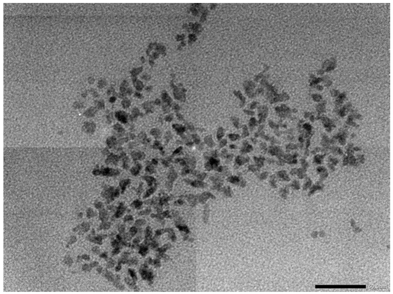
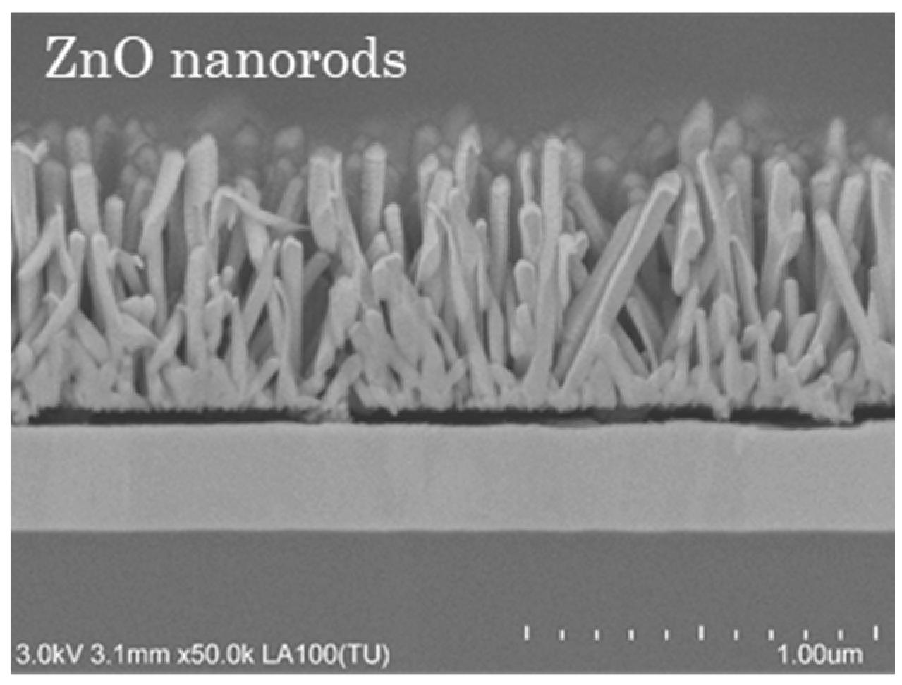
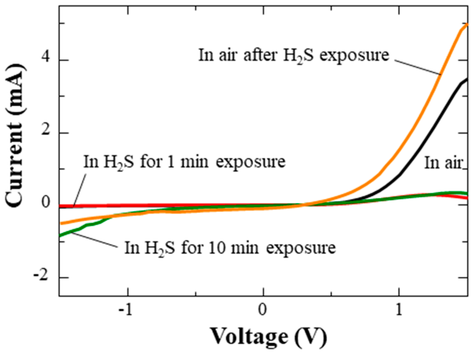
3. Results and Discussion

Figure1 shows a representative SEM image of ZnO NRs deposited on ITO. ZnO NRs grew perpendicular to the substrate to form a porous film. The diameter and the length of the NRs were estimated to be ca. 100 and 700 mm, respectively. Figure 2 shows a TEM image of CuO / Cu2O NCs. The size of the NCs is 8 to 10 nm with a narrow size distribution. XRD results revealed that Cu2O was converted into CuO after ligand exchange with an alkaline solution.
Figure 3 shows IV curves of the device, in which CuO NCs were deposited onto ZnO NRs, in air and air containing 8 ppm H2S at 150 °C. The device exhibited a clear rectification behavior in air at 150 °C, indicating that PN junctions were formed between CuO NCs and ZnO NRs. However, such a clear rectification behavior was lost under H2S atmosphere. The current in the forward and reverse directions significantly reduced after exposure to H2S. We have recently confirmed that CuO NCs-based sensors respond to H2S by an increase in electrical resistance due to reaction of adsorbed oxygen with H2S, representing a typical behavior of p-type semiconductors [3]. Thus, the observed increase in resistance for the present device is possibly due to surface reaction of adsorbed oxygen with H2S and the resulting annihilation of holes. The rectification of the current recovered by reintroduction of air, which possibly increased the electron concentration in CuO. On the other hand, at higher temperature, the device showed a simple ohmic behavior (no figure), suggesting that complete conversion of CuO into CuS occurred. Thus, the sensing mechanism should be dependent on temperature. The above results demonstrate the feasibility of nanorod/nanocrystal-based PN-junction devices in constructing gas sensors. Currently, a more detailed mechanism is under investigation.

Acknowledgments

This research was funded by a Grant-in-Aid for the Promotion of Joint International Research (15KK0189) from the Ministry of Education, Culture, Sports, Science and Technology of Japan.

Conflicts of Interest

The authors declare no conflict of interest.

References

  1. Tamaki, J.; Maekawa, T.; Miura, N. , Yamazoe, N. CuO-SnO2 element for highly sensitive and selective detection of H2S. Sens. Actuators B Chem. 1992, 3, 197–203. [Google Scholar] [CrossRef]
  2. Gaddam, V.; Kumar, R.R.; Parmar, M.; Nayak, M.M.; Rajanna, K. Synthesis of ZnO nanorods on a flexible Phynox alloy substrate: Influence of growth temperature on their properties. RSC Adv. 2015, 5, 89985–89992. [Google Scholar] [CrossRef]
  3. Mikami, K.; Kido, Y.; Akaishi, Y.; Quitain, A.; Kida, T. Synthesis of Cu2O/CuO nanocrystals and their application to H2S sensing. Sensers 2019, 19, 211. [Google Scholar] [CrossRef] [PubMed]
Figure 1. SEM image of ZnO nanorods deposited on an ITO substrate.
Proceedings 14 00026 g001
Figure 2. TEM image of CuO nanocrystals synthesized by a hot-soap method. The scale bar is 50 nm.
Proceedings 14 00026 g002
Figure 3. IV curves of the CuO NCs/ZnO NRs device in air and air containing 8 ppm H2S at 150 °C.
Proceedings 14 00026 g003

