Long-wavelength infrared (LWIR) focal plane arrays (FPAs) are of particular importance in thermal imaging, remote sensing, and defense applications due to their ability to detect thermal signatures in the 8–12 μm spectral range. Among various material systems under development for LWIR photodetectors, InAs/InAsSb type-II superlattices (T2SLs) have emerged as highly promising candidates, offering superior bandgap engineering flexibility, suppressed Auger recombination, and compatibility with mature III–V semiconductor processing [1,2,3,4].
To overcome the limitations of conventional photodiodes, particularly high dark current associated with surface leakage and Shockley–Read–Hall (SRH) generation, the nBn detector architecture has gained widespread attention. The nBn structure incorporates a wide-bandgap barrier layer between two n-type regions to effectively suppress bulk dark current while maintaining efficient collection of photo-generated carriers [5].
A key performance metric for LWIR detectors intended for integration into cooled FPAs is the dark current density, which must be sufficiently low to ensure background-limited infrared performance (BLIP) and compatibility with standard readout integrated circuits (ROICs). The so-called “Rule 07” provides a widely accepted empirical benchmark for dark current density as a function of cutoff wavelength and temperature [6]. Notably, properly designed nBn detectors based on InAs/InAsSb T2SLs are capable of achieving dark current levels that approach or even meet the Rule 07 limit, particularly at typical operating temperatures around 77 K [7,8].
This work presents an initial attempt at the design and optimization of nBn detectors using InAs/InAsSb T2SL absorbers tailored for LWIR FPA. Although the nBn design inherently eliminates depletion at the barrier interface, minimizing tunneling, generation and recombination (GR) noise and surface leakage current—key challenges in LWIR detection, practical implementations still exhibit some unwanted effects. We analyze the influence of material parameters on the device performance to identify and eliminate the issues.
The device epitaxial layer was grown on a three-inch GaAs (100) substrate using the molecular beam epitaxy (MBE) technique on a RIBER COMPACT 21 DZ system (Riber, Bezons, France). This equipment featured standard effusion cells for gallium (Ga), indium (In), and aluminum (Al), as well as “valved cracked” cells for arsenic (As) and antimony (Sb). The device utilizes an nBn design with an InAs/InAsSb T2SL active layer and an AlGaAsSb barrier. Absorber superlattice with a period of 8.96 nm and a total thickness of 0.8 μm optimized for a cutoff wavelength of about 9 μm at 80 K.
Figure 1 shows the spectral response of a photodetector measured at 80 K under three different bias voltages. The cut-off wavelength, defined as the wavelength at which the quantum efficiency (QE) drops to near zero, is approximately 8.5 µm, independent of the applied bias voltage. The QE increases significantly when a negative bias is applied, and saturates above –0.1 V. This suggests that the barrier in the valence band is well aligned.
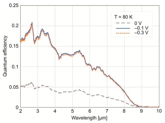
Figure 1.
Quantum efficiency (QE) as a function of wavelength for different bias voltages at a temperature of 80 K.
The dark current density versus voltage plots measured over a wide temperature range are presented in Figure 2. Each curve corresponds to a specific temperature from 40 K to 280 K in 20 K steps. The measurements were performed symmetrically in forward and reverse bias. The barrier structure reduces the tunneling and GR currents but does not eliminate them completely. This is better visible in the diagram for the dark current density versus temperature (Figure 3).
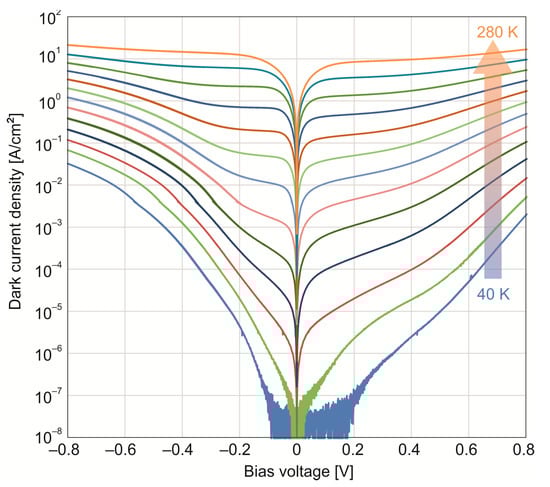
Figure 2.
Dark current density versus voltage for various temperatures in the range 40–280 K.
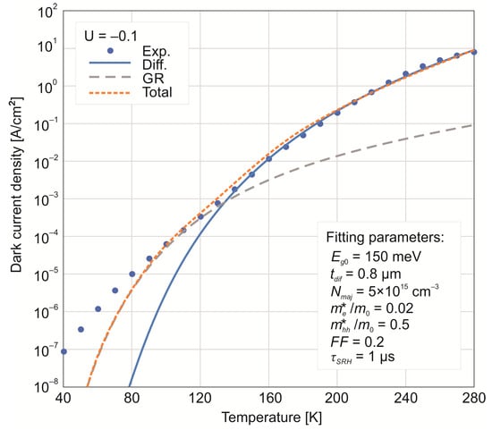
Figure 3.
Dark current density versus temperature.
The experimental results were fitted with an analytical model that takes into account the diffusion and GR currents. The diffusion current arises from the thermal generation of carriers in the undepleted semiconductor, and its density can be expressed as
where q is the electron charge, ni is the intrinsic carrier concentration, tdif is the diffusion region thickness, Nmaj is the majority carrier density, τA is the lifetime due to Auger recombination, and τSRH is the lifetime for recombination through SRH centers in the bandgap.
When the depletion region occurs within the absorber region, the additional depletion current component is visible. The GR current density can be expressed as
where W is the width of the depletion region.
The selected fitting parameters for absorber layer are shown in the inset of Figure 3. A detailed description of the model and parameters is described elsewhere [9,10].
In the high temperature range, the current is limited by the diffusion mechanism, while in the low temperature range, it is limited by the GR mechanism and an additional one, not included in the model, which may even be a surface leakage current [11]. The transition temperature between the diffusion current and GR is 130 K. At the target operating temperature of LWIR FPA (80 K), the dark current density is 1 A/cm2 at –1 V, which is two orders of magnitude higher than defined by the “Rule 07”. Eliminating the GR component by proper design of the nBn device can achieve this limit.
In conclusion, this study provides a comprehensive analysis of the LWIR photodetector’s performance across a wide range of temperatures. The nBn detector with a cut-off wavelength of 8.5 μm at 80 K shows an improved QE under reverse bias. Dark current analysis demonstrates the interplay between diffusion and GR mechanisms, with a transition temperature of 130 K. Analytical calculations show that there is potential for improvement through optimized nBn device design to achieve the “Rule 07” benchmark. Future work should focus on improving the barrier structure to further suppress tunneling and GR currents, potentially achieving performance levels comparable to current FPA standards.
Author Contributions
Conceptualization, M.K.; validation, K.M. (Krystian Michalczewski) and W.G.; investigation, G.K., P.B., K.M. (Krzysztof Murawski), Ł.K., B.S., K.S. and J.J.; resources, Ł.K., B.S., K.S. and J.J.; data curation, G.K., P.B. and K.M. (Krzysztof Murawski); writing—original draft preparation, M.K.; writing—review and editing, K.M. (Krystian Michalczewski) and W.G.; visualization, G.K. and P.B.; project administration, M.K.; funding acquisition, M.K. All authors have read and agreed to the published version of the manuscript.
Funding
This research was funded by The National Science Centre (Poland), grant number UMO-2023/51/B/ST7/02340.
Institutional Review Board Statement
Not applicable.
Informed Consent Statement
Not applicable.
Data Availability Statement
The data supporting this study are available from the corresponding author upon reasonable request (malgorzata.kopytko@wat.edu.pl).
Conflicts of Interest
The authors declare no conflicts of interest.
References
- Ting, D.Z.-Y.; Soibel, A.; Höglund, L.; Nguyen, J.; Hill, C.J.; Khoshakhlagh, A.; Gunapala, S.D. Type-II superlattice infrared detectors. In Semiconductors and Semimetals, 1st ed.; Gunapala, S.D., Rhiger, D.R., Jagadish, C., Eds.; Elsevier: Amsterdam, The Netherlands, 2011; Volume 84, pp. 1–57. [Google Scholar]
- Bürkle, L.; Fuchs, F. InAs/(GaIn)Sb superlattices: A promising material system for infrared detection. In Handbook of Infrared Detection Technologies; Henini, M., Razeghi, M., Eds.; Elsevier: Oxford, UK, 2002; pp. 159–189. [Google Scholar]
- Ting, D.Z.; Soibel, A.; Khoshakhlagh, A.; Keo, S.A.; Rafol, S.B.; Fisher, A.M.; Pepper, B.J.; Luong, E.M.; Hill, C.J.; Gunapala, S.D. Advances in III-V semiconductor infrared absorbers and detectors. Infrared Phys. Technol. 2019, 97, 210–216. [Google Scholar] [CrossRef]
- Rogalski, A.; Martyniuk, P.; Kopytko, M.; Madejczyk, P.; Krishna, S. InAsSb-based infrared photodetectors: Thirty years later on. Sensors 2020, 20, 7047. [Google Scholar] [CrossRef] [PubMed]
- Maimon, S.; Wicks, G. nBn detector, an infrared detector with reduced dark current and higher operating temperature. Appl. Phys. Lett. 2006, 89, 151109. [Google Scholar] [CrossRef]
- Tennant, W.E.; Lee, D.; Zandian, M.; Piquette, E.; Carmody, M. MBE HgCdTe technology: A very general solution to IR detection, described by ‘Rule 07’, a very convenient heuristic. J. Electron. Mater. 2008, 37, 1406–1410. [Google Scholar] [CrossRef]
- Ting, D.Z.-Y.; Soibel, A.; Khoshakhlagh, A.; Keo, S.A.; Fisher, A.M.; Rafol, S.B.; Höglund, L.; Hill, C.J.; Pepper, B.J.; Gunapala, S.D. Long wavelength InAs/InAsSb superlattice barrier infrared detectors with p-type absorber quantum efficiency enhancement. Appl. Phys. Lett. 2021, 118, 133503. [Google Scholar] [CrossRef]
- Canedy, C.L.; Aifer, E.H.; Vurgaftman, I.; Tischler, J.G.; Meyer, J.R.; Warner, J.H.; Jackson, E.M. Antimonide type-II “W” photodiodes with long-wave infrared R0A comparable to HgCdTe. J. Electron. Mater. 2007, 36, 852–856. [Google Scholar] [CrossRef]
- Kopytko, M.; Rogalski, A. Performance evaluation of type-II superlattice devices relative to HgCdTe photodiodes. IEEE Trans. Electron Devices 2022, 69, 2992–3002. [Google Scholar] [CrossRef]
- Kinch, M.A. State-of-the-Art Infrared Detector Technology, 1st ed.; SPIE Press: Bellingham, WA, USA, 2014; pp. 37–47. [Google Scholar]
- Nyga, M.; Bogudki, J.; Szawcow, O.; Kopytko, M. Ionic liquid as a novel surface passivation for InAs/InAsSb type-II superlattice infrared detector. J. Appl. Phys. 2025, 137, 175702. [Google Scholar] [CrossRef]
Disclaimer/Publisher’s Note: The statements, opinions and data contained in all publications are solely those of the individual author(s) and contributor(s) and not of MDPI and/or the editor(s). MDPI and/or the editor(s) disclaim responsibility for any injury to people or property resulting from any ideas, methods, instructions or products referred to in the content. |
© 2025 by the authors. Licensee MDPI, Basel, Switzerland. This article is an open access article distributed under the terms and conditions of the Creative Commons Attribution (CC BY) license (https://creativecommons.org/licenses/by/4.0/).