1. Introduction
Among different simulation models used, HIL simulation has become increasingly significant as a tool for evaluating and prototyping novel power electronic systems. Power electronic system development and testing can be costly and dangerous, particularly for high-power systems. To mitigate these risks, engineers often use HIL simulation to emulate a portion of a system in real time. Using this approach, they combine a computational device or simulator with physical components of the system for real-time simulation. Engineers can examine how a system design interacts with its physical components securely and cost-effectively without needing a physical prototype. The literature containing numerous examples of power electronic systems using HIL and real-time simulation applications can be found in [
1,
2,
3]. However, integrating high frequency, Silicon Carbide (Sic) based switching converters in current power electronic systems poses a challenge because to accurately depict their nonlinear dynamics, short real-time simulation time steps are required. These short time increments place strong constraints on the computing hardware used for the simulation. As a result, there has been a shift towards using FPGAs and Digital Signal Processors (DSPs), which have the ability to perform real-time computation in smaller time steps.
The use of HIL simulation on FPGAs for power electronics converters has become popular as it effectively addresses the difficulties [
4,
5,
6,
7] related to the complicated topology of these converters and enables higher switching frequencies [
8,
9,
10,
11,
12]. However, modeling power electronics converters using this technique can be difficult due to the circuit’s constantly changing topology [
13,
14,
15].
The detailed modeling of complex power system equipment has been successfully achieved using FPGAs, as demonstrated in the literature [
16,
17,
18,
19,
20,
21]. Despite the existence of nonlinear IGBT and diode models for some time, they have rarely been used in the hardware emulation of power converters due to their complexity. Instead, simpler switch models are more commonly used. The two-node architecture, which includes a current source in parallel with resistance [
22], has proven to be efficient in two-level voltage-sourced converters. Additionally, in other circuit simulations, the ideal switch model is often used. However, these IGBT and diode models only represent the on and off-state properties and are unable to provide additional data for converter testing. The Look-Up Table (LUT) approach and curve-fitting-based linear switch models [
23,
24] are used in these models to record the typical switching transients. However, the accuracy of this model is limited by the exclusion of non-linearities, and both models lack adaptability since the electromagnetic environment, along with the stored waveform shapes in the FPGA ROM, cannot be altered, which is typically the case in the gate driver circuit. This highlights the need for adaptable models.
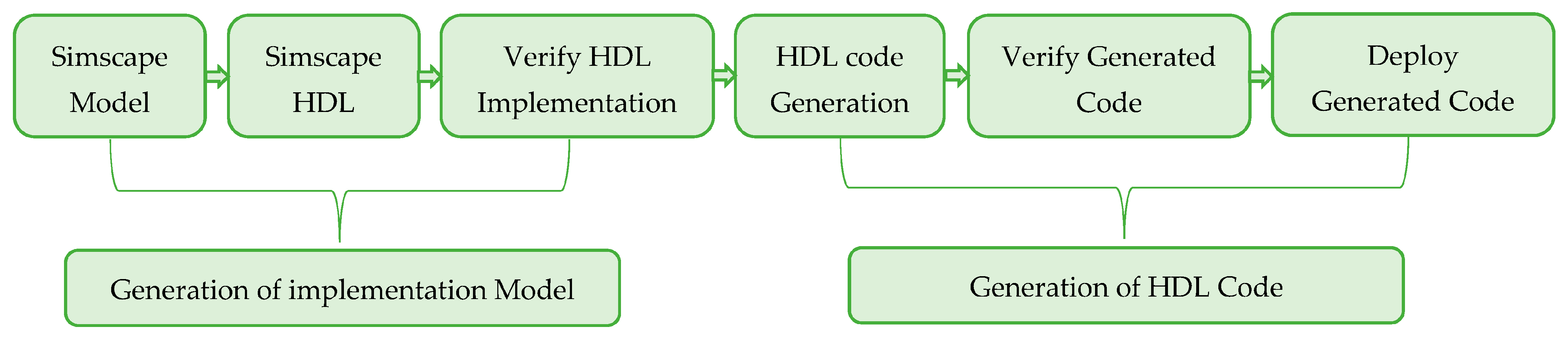
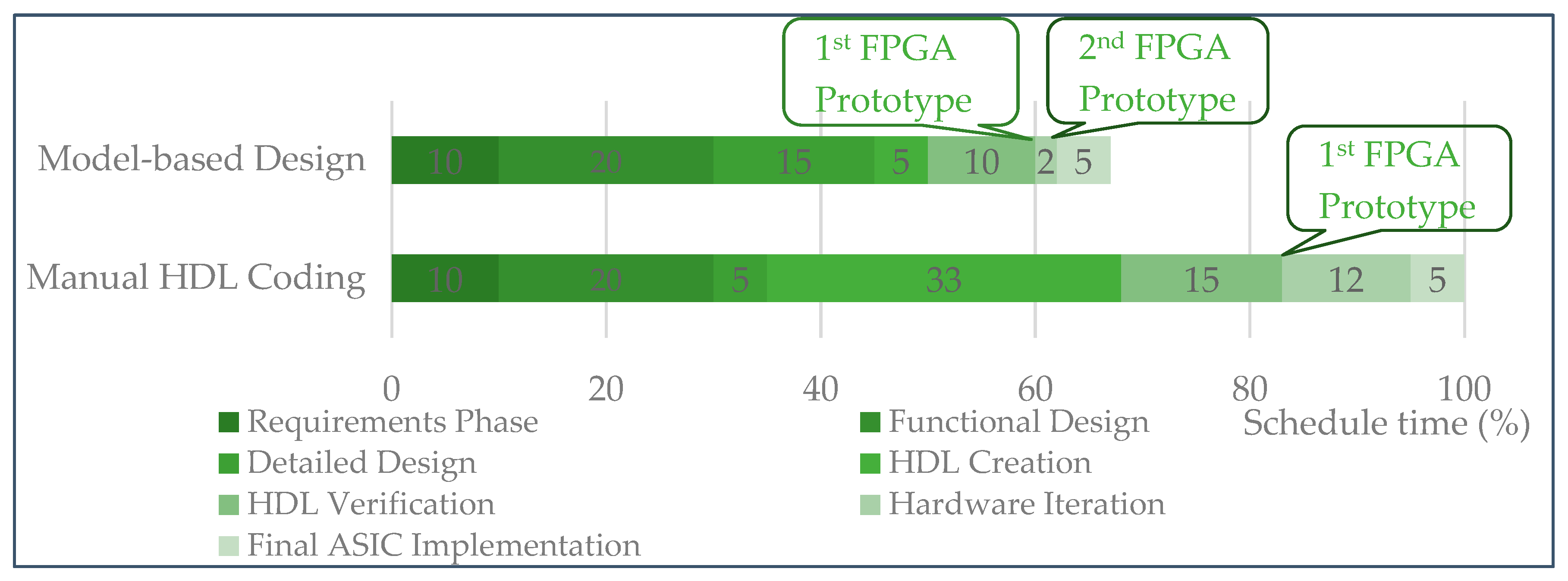
Furthermore, FPGA programming requires specialized knowledge of hardware description language (HDL), making it a demanding and time-consuming task. The HDL Coder tool provided in Matlab/Simulink can be used to generate automated HDL code from a model-based Simulink design, hence providing a faster alternative to hand coding (
Figure 1). This allows the engineers/developers to spend more time during the detailed design phase for creating higher-quality fixed-point algorithms. Reducing the need for extensive knowledge of HDL helps in speeding up the FPGA development process considerably [
25,
26,
27,
28].
The central contribution of this paper is to introduce a novel power diode and IGBT behavioral models for FPGA. These models are specifically designed for the real-time simulation of rapid transients in power electronics circuits, addressing the aforementioned problems in the models previously used. For automated HDL code generation, the HDL coder tool from Matlab/Simulink is used in this model.
The aim of this research is to propose a methodology and workflow for the hardware emulation of power converters based on FPGA, which includes nonlinear behavioral switch models. The emulation is conducted using the HDL Coder tool provided in Matlab/Simulink. The organization of the paper is outlined accordingly.
Section 2 describes the nonlinear behavioral device models.
Section 3 demonstrates the Methodology for power electronics using Matlab/Simulink to implement the two models in hardware. Two case studies focusing on the basic device-level simulation of a single IGBT and power diode to verify their hardware are elucidated in
Section 4. The conclusion is presented in
Section 5.
2. Non-Linear Behavioral Device Model
2.1. Power Diode Non-Linear Behavioral Model
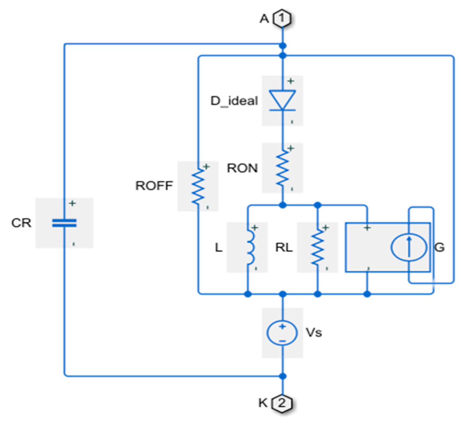
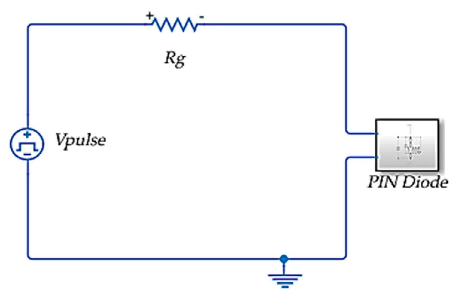
In the literature, a diode pin can be modeled as an equivalent circuit in
Figure 2. Reverse-biased diodes behave similarly to variable capacitors, which are modeled by voltage-controlled current sources with R
L and L [
29]; ROFF models the steady state of the diode during this period. R
ON represents the on-state resistance, while the voltage at the diode conduction threshold is denoted by VTH. The forward recovery current IF is established with a time constant imposed by the C
R capacitor. Notably, when the remaining charge is removed by the reverse current during the reverse recovery phase, the same capacitor interferes, generating oscillations of both current and voltage.
The expression for the reverse current during charge extraction by recombination is defined using the following:
where
t0 represents the time when the reverse current reached zero.
At the moment of the second discharge, the representation of the reverse current variation is expressed as follows:
where
=
L/
RL is the time constant, and
t1 is the moment the current crosses
IRRM.
A development of (1) and (2), together with the formula for the softness factor
s, yields Equation (3) for the maximum reverse current
IRRM, as well as Formulas (4) and (5) for
tL and the transconductance of the voltage-controlled current source.
G is calculable from [
30]:
For the
L inductor to remain unaffected by conduction, the
CF capacitor’s energy must be larger than the
L inductor’s energy.
Therefore, the inductance
L needs to check the following:
Manufacturers offer essential data, which may be utilized to identify all parameters using the equations presented in this section. These characteristics are derived from standard circumstances.
2.2. IGBT Behavioral Model
IGBTs have become a popular switching device in many power electronics applications due to their low conduction losses and high switching speeds. An accurate model of an IGBT is essential for analyzing and predicting various device and circuit characteristics, such as transients and power loss. Hefner’s physics-based model [
31,
32], widely regarded as one of the most comprehensive analytical IGBT models, has been adopted [
33] in well-known circuit-level simulators like Saber and PSpice.
This work builds on the model developed in [
34,
35]; the modeling of IGBT under MATLAB/SIMULINK is based on behavioral analysis. This type of modeling consists of replacing the power component with an electrical network composed of elements such as inductances, resistors, capacities, current and voltage generators, etc. Each element or set of elements in this network reflects a physical phenomenon. This type of model is simpler than analytical and numerical models, as its purpose is not to replicate the various physical phenomena of the semiconductor component. The electric model adapted was examined under the simulators of PSPICE and SABER in previous studies [
36]. The proposed model considers the IGBT’s static function as well as its transient behavior resulting from the impact of nonlinear inter-electrode capacities.
According to [
34], the electric IGBT model is a hybrid transistor that incorporates the advantages of both a Metal Oxide Semiconductor Field Effect Transistor (MOSFET) at its input and a BJT at its output. This results in the IGBT having high voltage-handling capabilities, low conduction losses of the BJT, and low power control advantages of the MOSFET. The developed model can predict both the static and dynamic behavior of the IGBT. Furthermore, the parameterization of the IGBT can be carried out easily using manufacturer data. This model represents the optimal balance between accuracy and simulation complexity.
2.2.1. Static IGBT Model
The following components make up the static MOSFET model:
Jmos: The controlled current source (Imos) represents the drain current.
VTH: DC voltage source represents the threshold voltage.
RGE: Resistance of the Leakage gate-emitter.
RDN: The resistive characteristic of the MOSFET channel, characterized by drain resistance.
DG: Diode permits the transition from the off to the on state.
DDC: An anti-parallel body diode is represented by a binary resistance RONDC/ROFFDC. It permits the transition from the linear to the saturated zone.
According to three scenarios, the VGE voltage controls the MOSFET current:
VGE < VTH: The transistor is off,
VGE + VCE0 − VTH > VCE is expressed below.
where
θ is the correction factor that accounts for the transverse field in the MOSFET channel, and
Kp is the transconductance.
The static BJT model for the bipolar component consists of the following:
VCE0 is the voltage threshold for the conduction of the base-emitter junction;
DP and DE represent base-collector junctions and the base-emitter, respectively;
β is the bipolar gain;
JPNP is a controlled current source that indicates the bipolar transistor’s current gain.
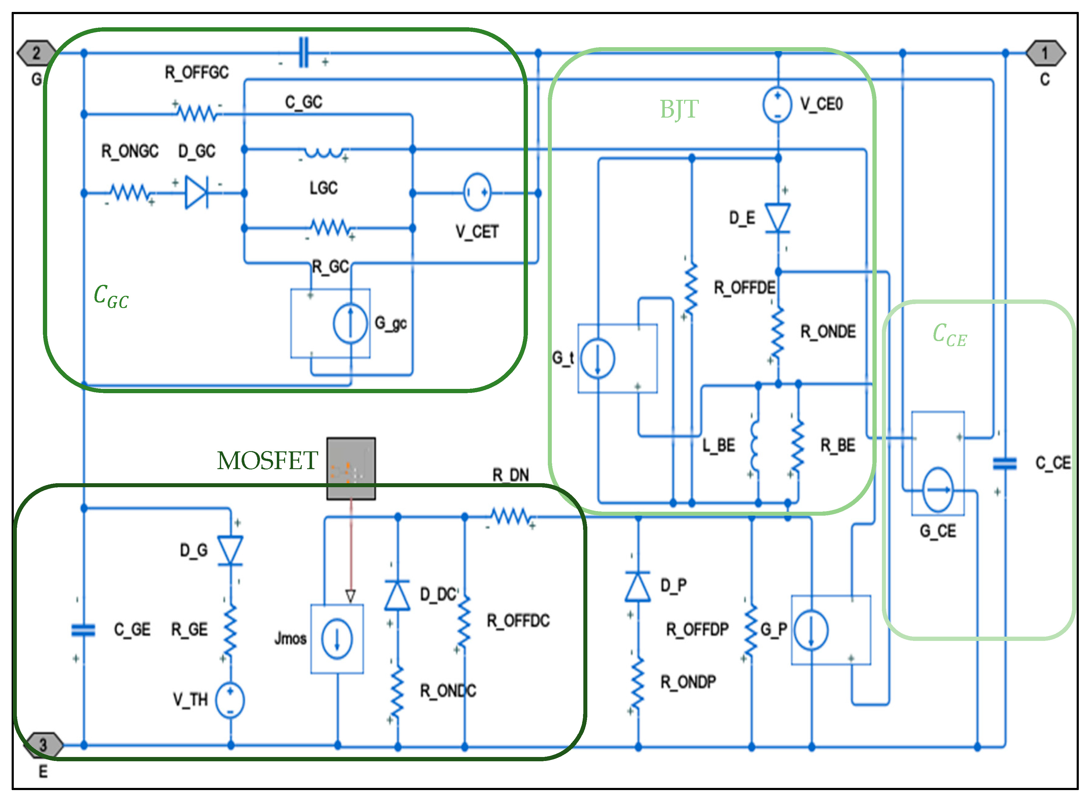
2.2.2. Dynamic IGBT Model
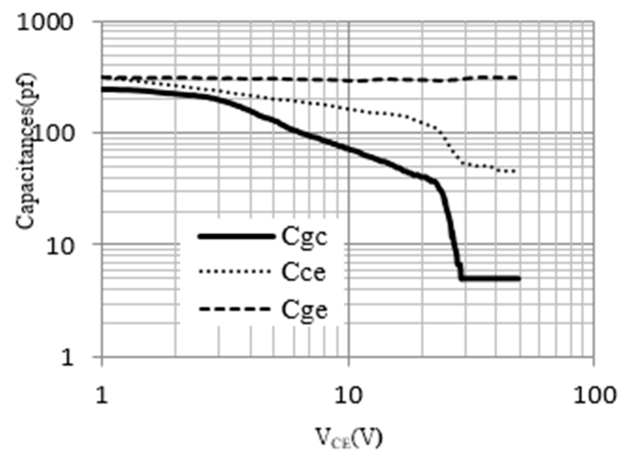
The static model is expanded with additional components to describe the dynamic behavior of the IGBT. These components include voltage-controlled current sources and non-linear terminal capacitances, representing the load responsible for the tail current (IC) during the turn-off state of the IGBT.
By removing one or two capacitors, constructors offer measuring capacitors between two terminals. The following Equation (11) may be used to calculate the values of the inter-electrode capacitances
CGE,
CCE, and
CGC using the reverse transfer capacitance (
CRE), the input capacitance (
CIE), and output capacitance (
COE).
The curve of the
CGE,
CCE, and
CGC capacitances is shown in
Figure 3.
Figure 4 depicts the modified model for these nonlinear capacitances.
The following equations are used to determine the coupling coefficients
GGC and
GCE:
The following equations are used to calculate the
CGC capacity parameters:
The CCE parameters are calculated using Equations (6)–(8).
The bipolar component is approximated by a controlled current source
Gt (
Figure 4), where Equation (17) provides the coupling coefficient
Gt:
where
CBE denotes the bipolar component that stores charges,
CBERonDE =
toff.
toff is determined using device datasheets.
Figure 4 depicts the investigated IGBT model.
The parameters for the model under investigation are obtained from technical specifications, established mathematical formulas, and then fine-tuned using a stochastic algorithm within Matlab [
34].
3. Design Methodology for Power Electronics
FPGAs are programmable logic devices composed of numerous simple logic elements (LEs). A high-speed Hardware Description Language (VHDL) can be used to program these LEs. The VHDL code is used to form logical functions by connecting individual LEs. Signal propagation delays and the number of LEs used are the main constraints of FPGA technology, but advancements in FPGAs have reduced propagation latency and increased the number of LEs available. The current market leaders in FPGA technology are AMD and Altera, offering various FPGA boards and kits.
Simscape HDL Workflow Advisor and HDL Coder are able to generate HDL code from the Simscape model for deploying on FPGA hardware. The Advisor translates the Simscape model to a Simulink implementation model that HDL Coder uses to generate HDL code.
Converting the Simscape model to HDL code enables the following:
Leverage the physical system modeling capabilities of Simscape;
Rapidly prototype models using the configuration and parallelism capabilities of the FPGA;
Simulate the HDL implementation in real time with hardware-in-the-loop (HIL).
Before executing the Simscape HDL Workflow Advisor, the network must be configured to rule out delays and execution parameters that are enabled.
The complex physical systems can be modeled and deployed in Simscape while converting the models into HDL code.
Figure 5 shows the workflow diagram of the functionalities at various stages:
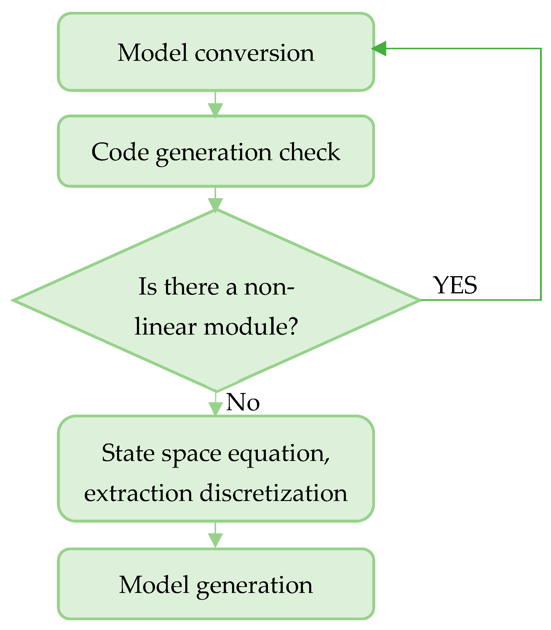
Each module must leverage the physical models in the Simscape library to guarantee the generation of HDL code for FPGA calls. While building the model, non-nonlinear modules cannot be used. The backward Euler method is adopted using the numerical integration algorithm.
3.1. State Space Model Generation
Before translating the Simscape model to an HDL low-level model, simulation verification must be performed after its successful development. The conversion of the physical model to a corresponding state-space model can be achieved by enabling HDL Workflow Advisor by typing “sschdladvisor(gcs)” on the MATLAB command. The configuration of the Configuration Solver must be examined to determine whether the Simscape model contains nonlinear modules or not. The same flow chart in
Figure 6 illustrates the conversion procedure. The state space equation is then extracted and discretized. Once the discrete state space model is constructed, the program identifies the number of valid modes in the Simscape model and its input and output states.
Once the HDL algorithm is validated, comparing the functionality of the HDL implementation model to the original Simscape algorithm, then HDL code can be generated for the implementation model. Using makehdl (‘gmStateSpaceHDL_current_model/HDL Subsystem’) MATLAB command prompt.
3.2. FPGA in the Loop Model Generation
Researchers widely use simulation tools that give the ideal tools to simulate any system without the risk of damage. The simulation is carried out via electronic design automation (EDA). The EDA simulator link presents a verification interface between the HDL simulator (and FPGA board) and Simulink (Matlab) tools. Using co-simulation, the verification operation between the Verilog HDL design and the Matlab/Simulink model is achieved. Using the EDA simulator link allows researchers to implement hardware verification on the FPGA board using FPGA in the loop (FIL) simulation. The Matlab/Simulink environment provides the toolbox and functions for HDL and FIL.
FIL has both hardware and software benefits and their approach. The FIL utilized the capabilities of Matlab/Simulink during co-simulation processing. The algorithm runs in real time when loaded on the FPGA board using FIL. During FIL processing, system components like power electronics, sensors, and other electrical elements are simulated on Matlab/Simulink.
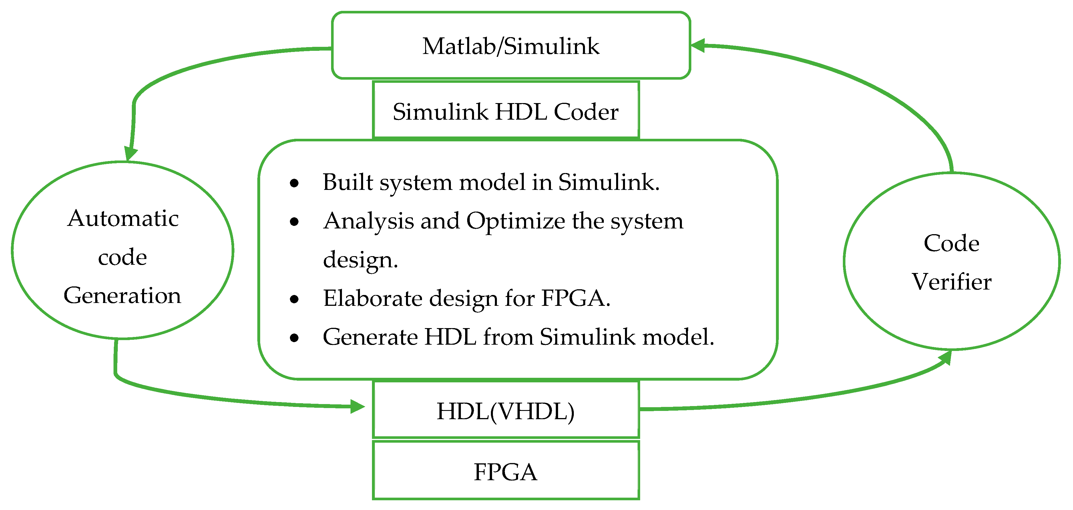
HDL describes electronic circuits in terms of the circuit’s operation, design, and tests to verify its operation using simulation. At the first step of the code conversion process, the new design ideas and algorithms are represented in terms of mathematical models and are tested in MA TLAB/Simulink floating point data types. The real HDL code generation process starts by modeling the model in MATLAB Simulink using an HDL Coder library. The components and blockset supported in HDL Coder can be found by typing hdllib in the command window.
Figure 7 shows the code conversion and verification process in MATLAB Simulink HDL Coder.
Once the Simulink model is created, HDL Workflow Advisor guides in a step-by-step process to generate code from the model. Moreover, it helps to check various other parameters and setting that is required for optimal code generation and verification.
The following steps in the HDL Workflow Advisor are essential and should be performed with caution [
37].
- ➢
Set Target Device and Synthesis Tool: You must select the correct target platform for your project. If you are using a custom board that is not supported by the Matlab Add-Ons, you must first install a custom board definition before you can proceed.
- ➢
Set Target frequency: You need to choose the clock frequency that will be used in the code that will be generated for the FPGA. This frequency can usually be set to the highest sampling frequency used in the code, which is the time it takes the FPGA to sample a signal.
- ➢
Prepare Model for HDL Code Generation: Follow the steps and accept the changes that are proposed. An error called “Abnormal exit” may occur during these steps. This problem is related to the Scope, and it can be resolved by erasing the Scope.
- ➢
Check Block Compatibility: If delay balancing is enabled globally, this task does not require any user input. However, if delay balancing is disabled globally and only enabled locally, a warning will be generated during this step. To avoid the verification from being blocked, the “Ignore warnings” option must be set.
- ➢
FPGA-in-the-loop Implementation: This section allows you to customize the FPGA-in-the-loop process. You can add additional files to the table below, such as HDL Coder black-box source code, custom FPGA design tool scripts, and/or constraint files. The last step of the process is to build the FPGA-in-the-loop code. This step can sometimes fail, even if all of the previous steps were successful. The most common problems are VHDL syntax errors, insufficient disk space, or insufficient permissions to write to the folder.
- ➢
Program Target Device: This step facilitates the loading of the bitstream onto the FPGA. The loading process can be accomplished either using a JTAG connection or by employing a network connection to the host computer via the “Download” option.
The generated HDL code is implemented on the FPGA. The Simulink reference model simultaneously sends input signals to the FPGA, and its output signals are returned from the FPGA. The board must be properly connected to the computer. Connections can be made using a JTAG-USB cable, Ethernet cable, or PCI-Express, depending on the board. The output signals from the FPGA are feedback to Simulink. This involves generating the input signals to the FPGA and analyzing its output signals in Simulink. With the FPGA in the loop, you can compare the implementation in the FPGA with the Simulink reference model. The HDL Workflow Advisor enables you to choose the board and create the system in Simulink. You can select one of the supported boards or customize the board you want to use. This technique provides the advantage of testing the system on the FPGA without the need for oscilloscopes or logic analyzers.
4. Case Study and Validation
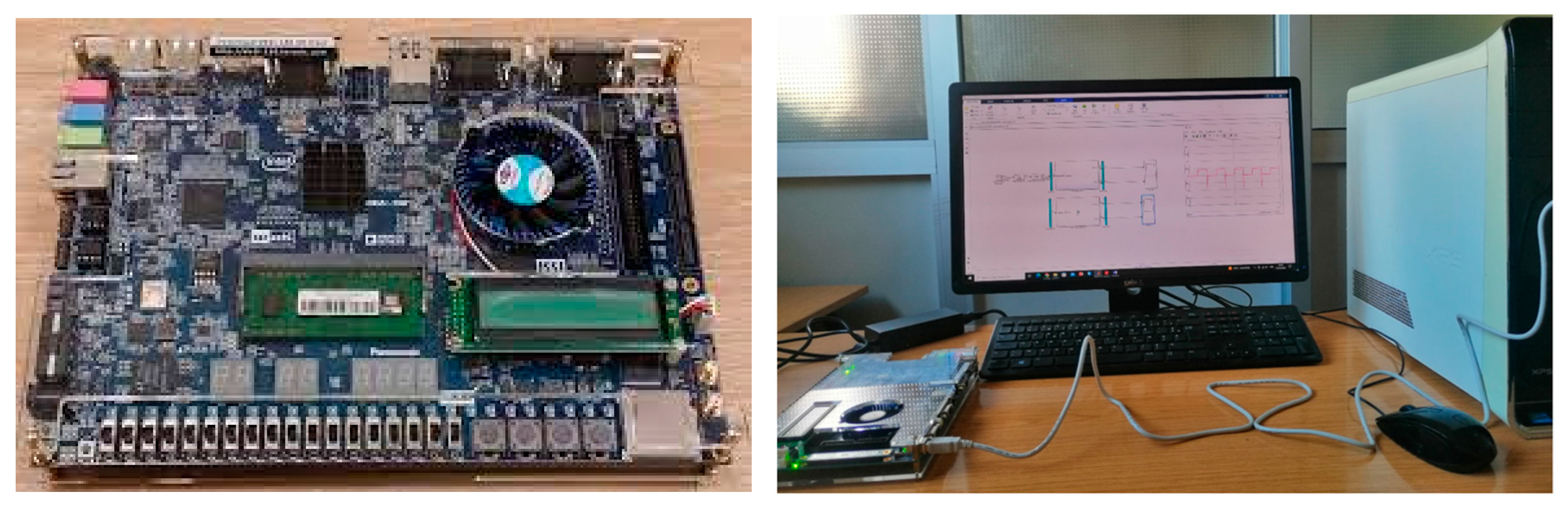
To validate the VHDL code of this case study, we use the DE1-SoC board from Altera. A combination of necessary technical details was compiled using the User Manual [
38]. Once the code is generated and loaded onto Fpga, it is time to test it by running the simulation (
Figure 8).
4.1. Single Diode
As illustrated in
Figure 9, the diode turn-on and turn-off transient characteristics as well as the DC mode behaviors are achieved using a resistance load and a square wave voltage source. The test circuit and diode parameters are shown in
Table 1. Actually, the diode utilized in this circuit is already illustrated in
Figure 2. The board resource usage of the circuit implementation is listed in
Table 2.
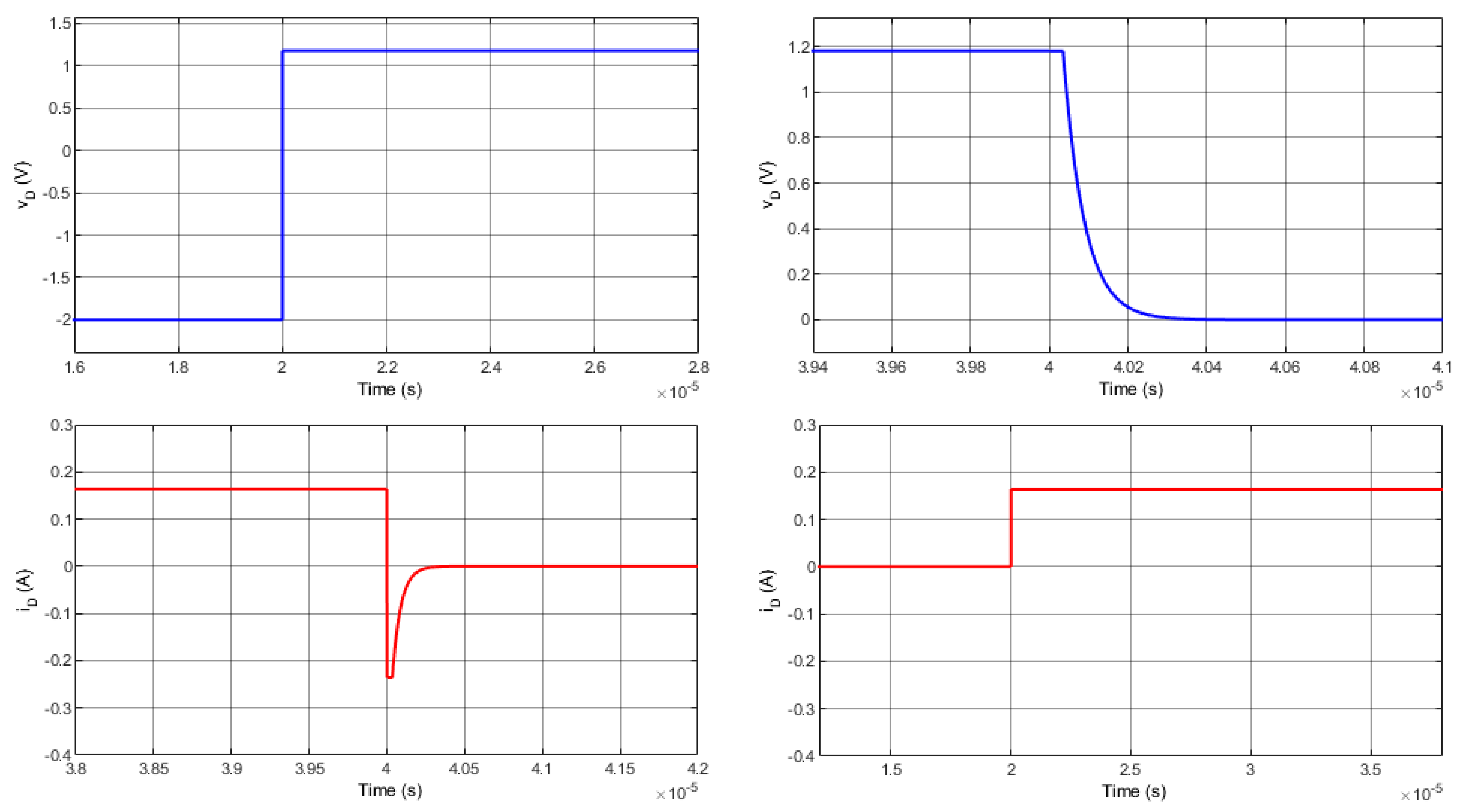
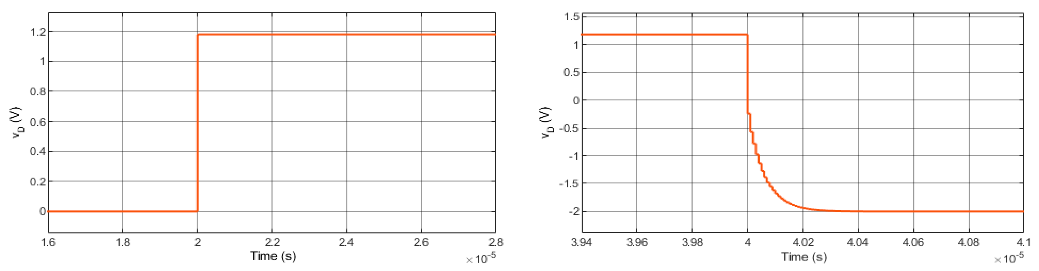
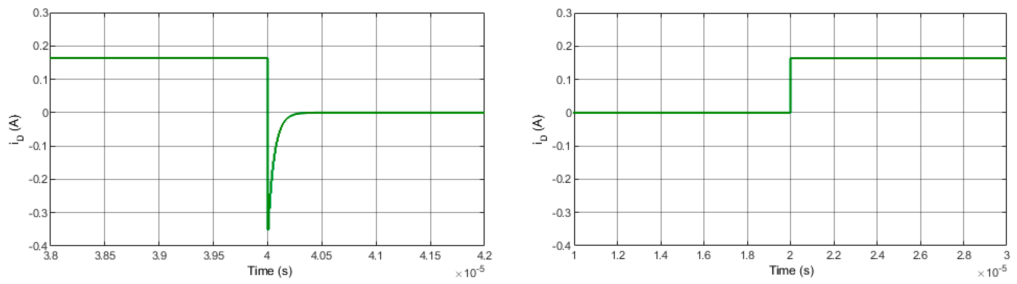
The steady-state results and transient-state results using Matlab toolbox and FIL are shown in
Figure 10 and
Figure 11. The current and voltage diode results using the FIL are the same as the results using the Matlab toolbox. In addition, diode transient-state results acquired are compared to those of Simulink. As seen, the FPGA-based loop simulation results are similar to the outputs of the Simulink simulation.
4.2. Single IGBT
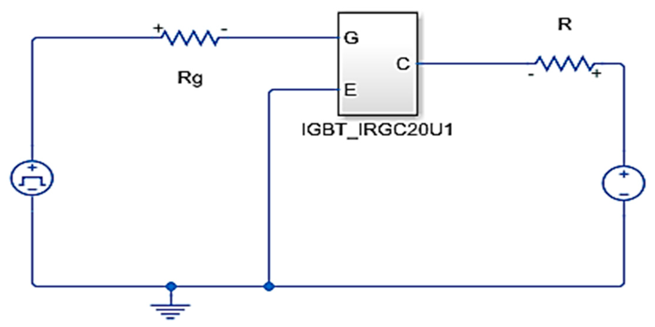
This case study focuses on the basic device-level simulation of an IGBT to validate its hardware model. As shown in
Figure 12, with a resistance load, a square wave voltage source at the gate, and a DC voltage source in the test circuit, the IGBT steady-state behaviors as well as the turn-on and turn-off transient characteristics can be observed. The IGBT device selected in this circuit is the IRGBC20U (
Figure 4). The test circuit and diode parameters are shown in
Table 3. The board resource usage of the circuit implementation is listed in
Table 4.
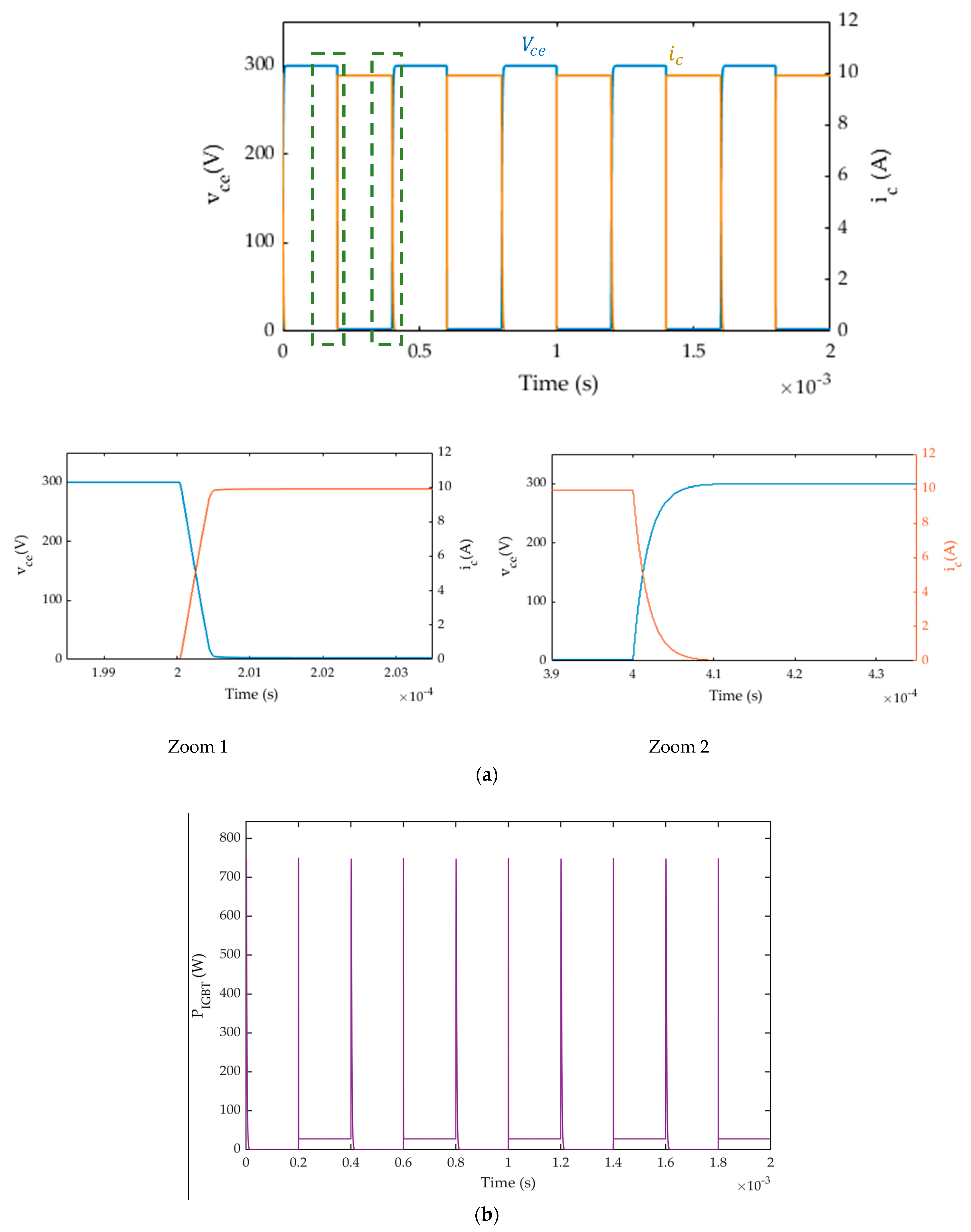
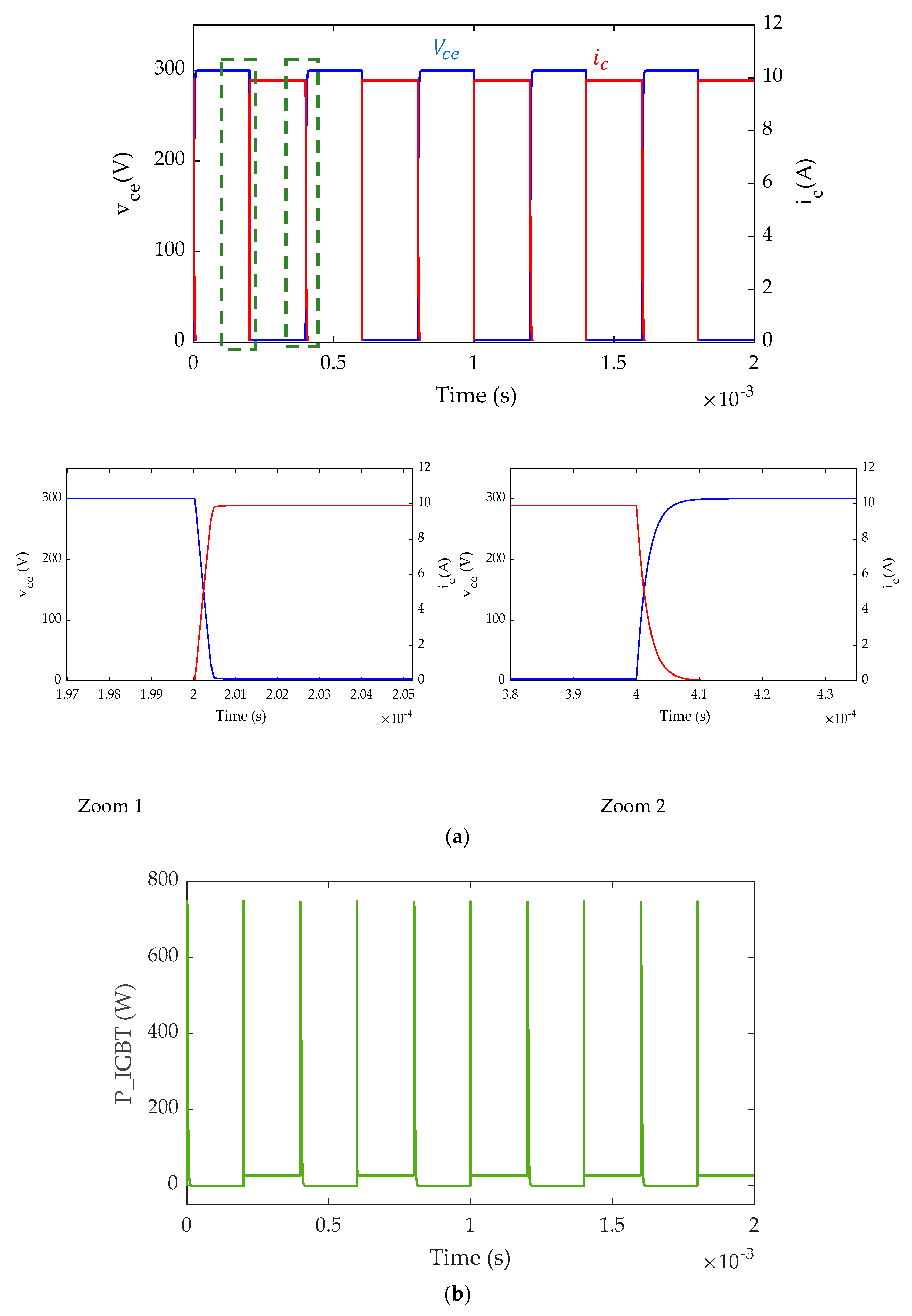
The steady-state voltage, steady-state collector current, and IGBT instantaneous power dissipation results using the Matlab toolbox and FIL are shown in
Figure 13 and
Figure 14. The transient-state voltages and currents results using the FIL are the same as the results using the Matlab toolbox. In addition, the transient-state voltages and currents results acquired are compared to those of Simulink. As seen, the FPGA-based loop simulation results are similar to the outputs of the Simulink simulation.
5. Conclusions
In this paper, we presented a method for hardware emulation of a device-level nonlinear behavioral IGBT model and power diode. The proposed method uses the HDL Workflow Advisor and Simscape tool to convert the HDL Subsystem to an FPGA and the simulation model to a state space model. This approach reduces development time and costs, and it also enables FPGA in-loop simulation without the need for a challenging hardware programming language.
The proposed method was verified via a circuit simulation in Matlab/Simulink. The results showed that the hardware emulation was in agreement with the simulation results, and it also had a faster performance on an FPGA compared to an offline computer program.
The proposed method is a valuable tool for the design and optimization of power electronic circuits. It allows designers to simulate the behavior of the circuit with a high degree of accuracy, which can help to ensure that the circuit will operate as desired.
The proposed method is also a promising approach for future research on FPGA code automation and power electronics transient simulation.
Author Contributions
Conceptualization, M.B. and E.E.; methodology, M.B. and E.E.; software, M.B.; validation, M.B., I.A.A. and E.E.; formal analysis, M.B. and E.E.; data curation, M.B. and E.E.; writing—original draft preparation, M.B.; writing—review and editing, E.E. and I.A.A. All authors have read and agreed to the published version of the manuscript.
Funding
This research received no external funding.
Data Availability Statement
Not applicable.
Conflicts of Interest
The authors declare no conflict of interest.
References
- Bin, L.; Wu, X.; Figueroa, H.; Monti, A. A low-cost real-time hardware in-the-loop testing approach of power electronics controls. IEEE Trans. Ind. Electron. 2007, 54, 919–931. [Google Scholar]
- Yunwei, L.; Vilathgamuwa, D.; Chiang, L.P. Design, analysis, and real-time testing of a controller for multibus microgrid system. IEEE Trans. Power Electron. 2005, 19, 1195–1204. [Google Scholar]
- Ivanović, Z.R.; Adžić, E.M.; Vekić, M.S.; Grabić, S.U.; Čelanović, N.L.; Katić, V.A. HIL evaluation of power flow control strategies for energy storage connected to smart grid under unbalanced conditions. IEEE Trans. Power Electron. 2012, 27, 4699–4710. [Google Scholar] [CrossRef]
- Zhang, B.; Hu, R.; Tu, S.; Zhang, J.; Jin, X.; Guan, Y.; Zhu, J. Modeling of Power System Simulation Based on FRTDS. Energies 2018, 11, 2749. [Google Scholar] [CrossRef]
- Leng, F.; Mao, C.; Wang, D.; An, R.; Zhang, Y.; Zhao, Y.; Cai, L.; Tian, J. Applications of Digital-Physical Hybrid Real-Time Simulation Platform in Power Systems. Energies 2018, 11, 2682. [Google Scholar] [CrossRef]
- Zamiri, E.; Sanchez, A.; Yushkova, M.; Martínez-García, M.S.; de Castro, A. Comparison of different design alternatives for hardware-in-the-loop of power converters. Electronics 2021, 10, 926. [Google Scholar] [CrossRef]
- Matar, M.; Iravani, R. FPGA Implementation of the Power Electronic Converter Model for Real-Time Simulation of Electromagnetic Transients. IEEE Trans. Power Deliv. 2010, 25, 852–860. [Google Scholar] [CrossRef]
- Zhang, B.; Wang, Y.; Tu, S.; Jin, Z. FPGA-Based Real-Time Digital Solver for Electro-Mechanical Transient Simulation. Energies 2018, 11, 2650. [Google Scholar] [CrossRef]
- Li, J.; Li, X.; Du, L.; Cao, M.; Qian, G. An Intelligent Sensor for the Ultra-High-Frequency Partial Discharge Online Monitoring of Power Transformers. Energies 2016, 9, 383. [Google Scholar] [CrossRef]
- Zhang, B.; Wu, Y.; Jin, Z.; Wang, Y. A Real-Time Digital Solver for Smart Substation Based on Orders. Energies 2017, 10, 1795. [Google Scholar] [CrossRef]
- Zhang, B.; Nie, S.; Jin, Z. Electromagnetic Transient-Transient Stability Analysis Hybrid Real-Time Simulation Method of Variable Area of Interest. Energies 2018, 11, 2620. [Google Scholar] [CrossRef]
- Stifter, M.; Cordova, J.; Kazmi, J.; Arghandeh, R. Real-Time Simulation and Hardware-in-the-Loop Testbed for Distribution Synchrophasor Applications. Energies 2018, 11, 876. [Google Scholar] [CrossRef]
- Benhalima, S.; Miloud, R.; Chandra, A. Real-Time Implementation of Robust Control Strategies Based on Sliding Mode Control for Standalone Microgrids Supplying Non-Linear Loads. Energies 2018, 11, 2590. [Google Scholar] [CrossRef]
- Garcia, J.; Garcia, P.; Capponi, F.G.; Donato, G.D. Analysis, Modeling, and Control of Half-Bridge Current-Source Converter for Energy Management of Supercapacitor Modules in Traction Applications. Energies 2018, 11, 2239. [Google Scholar] [CrossRef]
- Priyadarshi, N.; Padmanaban, S.; Lonel, D.M.; Mihet-Popa, L.; Azam, F. Hybrid PV-Wind, Micro-Grid Development Using Quasi-Z-Source Inverter Modeling and Control—Experimental Investigation. Energies 2018, 11, 2277. [Google Scholar] [CrossRef]
- Chen, Y.; Dinavahi, V. Hardware emulation building blocks for large-scale real-time simulation of power grids. IEEE Trans. Ind. Inf. 2014, 10, 373–381. [Google Scholar] [CrossRef]
- Liu, J.; Dinavahi, V. A real-time nonlinear hysteretic transformer transient model on FPGA. IEEE Trans. Ind. Electron. 2014, 61, 3587–3597. [Google Scholar] [CrossRef]
- Tavana, N.R.; Dinavahi, V. A general framework for real-time simulation of electrical machines on FPGA for HIL applications. IEEE Trans. Ind. Electron. 2015, 62, 2041–2053. [Google Scholar] [CrossRef]
- Caseiro, L.; Caires, D.; Mendes, A. Prototyping Power Electronics Systems with Zynq-Based Boards Using Matlab/Simulink—A Complete Methodology. Electronics 2022, 11, 1130. [Google Scholar] [CrossRef]
- Liu, J.; Dinavahi, V. Detailed magnetic equivalent circuit based real-time nonlinear power transformer model on FPGA for electromagnetic transient studies. IEEE Trans. Ind. Electron. 2016, 63, 1191–1202. [Google Scholar] [CrossRef]
- Tavana, N.R.; Dinavahi, V. Real-time nonlinear magnetic equivalent circuit model of induction machine on FPGA for hardware-in-the-loop simulation. IEEE Trans. Energy Convers. 2016, 31, 520–530. [Google Scholar] [CrossRef]
- Herrera, L.; Li, C.; Yao, X.; Wang, J. FPGA-based detailed real-time simulation of power converters and electric machines for EV HIL applications. IEEE Trans. Ind. Appl. 2015, 51, 1702–1712. [Google Scholar] [CrossRef]
- Shen, Z.; Dinavahi, V. Real-time device-level transient electrothermal model for modular multilevel converter on FPGA. IEEE Trans. Power Electron. 2016, 31, 6155–6168. [Google Scholar] [CrossRef]
- Wong, C. EMTP modeling of IGBT dynamic performance for power dissipation estimation. IEEE Trans. Ind. Appl. 1997, 33, 64–71. [Google Scholar] [CrossRef]
- van Beek, S.; Sharma, S.; Prakash, S. Four Best Practices for Prototyping MATLAB and Simulink Algorithms on FPGAs. Verif. Horiz. 2012, 8, 6. [Google Scholar]
- Versen, M.; Kipfelsberger, S.; Soekmen, F. Model-Based Reference Design Projects with MathWorks’ HDL Workflow Advisor for Custom-Specific Electronics with the Zedboard. In Proceedings of the ANALOG 2016; 15. ITG/GMM-Symposium, Bremen, Germany, 12–14 September 2016; pp. 1–4. [Google Scholar]
- Siwakoti, Y.P.; Town, G.E. Design of FPGA-controlled Power Electronics and Drives Using MATLAB Simulink. In Proceedings of the 2013 IEEE ECCE Asia Downunder, Melbourne, VIC, Australia, 3–6 June 2013; pp. 571–577. [Google Scholar]
- Sumam, M.; Shiny, G. Rapid Prototyping of High Performance FPGA Controller for an Induction Motor Drive. In Proceedings of the 2018 8th International Conference on Power and Energy Systems (ICPES), Colombo, Sri Lanka, 21–22 December 2018; pp. 76–80. [Google Scholar]
- Mijlad, N.; Elwarraki, E.; Elbacha, A. SIMSCAPE electro-thermal modelling of the PIN diode for power circuits simulation. IET Power Electron. 2016, 9, 1521–1526. [Google Scholar] [CrossRef]
- Elwarraki, E.; Sabir, A. Pspice behavior and thermal modeling of the PIN diode: A circuit approach. In Proceedings of the 14th IEEE International Conference on Electronics, Circuits and Systems, Marrakech, Morocco, 11–14 December 2007; pp. 1031–1034. [Google Scholar]
- Hefner, A.R.; Diebolt, D.M. An experimentally verifed IGBT model implemented in the Saber circuit simulator. IEEE Trans. Power Electron. 1994, 9, 532–542. [Google Scholar] [CrossRef]
- Hefner, A.R. Modeling buffer layer IGBTs for circuit simulation. IEEE Trans. Power Electron. 1995, 10, 111–123. [Google Scholar] [CrossRef]
- Oziemkiewicz, G.T. Implementation and Development of the NIST IGBT Model in a SPICE-Based Commercial Circuit Simulator. Ph.D. Thesis, Department of Electrical and Computer Engineering, University of Florida, Gainesville, FL, USA, 1995. [Google Scholar]
- Baghdadi, M.; Elwarraki, E.; Mijlad, N.; Ait Ayad, I. SIMSCAPE electrical modelling of the IGBT with parameter optimization using genetic algorithm. J. Electr. Comput. Eng. 2021, 2021, 6665384. [Google Scholar] [CrossRef]
- Mijlad, N.; Elwarraki, E.; Elbacha, A. Implementation of a behavioral IGBT model in SIMULINK. In Proceedings of the International Conference on Electrical and Information Technologies (ICEIT), Marrakech, Morocco, 25–27 March 2015; pp. 129–133. [Google Scholar]
- Elwarraki, E.; Sabir, A. Behavioural and electrothermal modelling of the IGBT for circuits simulation. In Proceedings of the 14th IEEE International Conference on Electronics, Circuits and Systems, Marrakech, Morocco, 11–14 December 2007; pp. 90–93. [Google Scholar]
- Mathworks. Getting Started with Altera FPGA Platform—MATLAB & Simulink. Available online: https://www.mathworks.com/help/hdlcoder/ug/getting-started-with-hardware-software-codesignworkflow-for-intel-soc (accessed on 10 January 2023.).
- DE2i-150 FPGA Development Ki. Available online: https://www.terasic.com.tw/cgibin/page/archive.pl?Language=English&CategoryNo=11&No=529&PartNo=2#contents (accessed on 15 December 2022.).
| Disclaimer/Publisher’s Note: The statements, opinions and data contained in all publications are solely those of the individual author(s) and contributor(s) and not of MDPI and/or the editor(s). MDPI and/or the editor(s) disclaim responsibility for any injury to people or property resulting from any ideas, methods, instructions or products referred to in the content. |
© 2023 by the authors. Licensee MDPI, Basel, Switzerland. This article is an open access article distributed under the terms and conditions of the Creative Commons Attribution (CC BY) license (https://creativecommons.org/licenses/by/4.0/).


