1. Introduction
Largest share of the today’s photovoltaic market belongs to crystalline silicon (c-Si) cells. The main advantages of this technology stem from basic properties of Si such as ideal band gap, durability, abundance, stability, and being environmentally friendly. However, the place of Si-cell technology is still limited in the world energy market. The most important reason is high material cost. To that end, the thin film technology is one of prominent solutions for reducing fabrication cost of Si based devices [
1,
2,
3]. Producing pc-Si thin films by means of in situ laser crystallization (LC) on various substrates draws attention in the electronic industry, especially for Si based TFTs and solar cell applications. In situ LC process is an adequate and cost-effective method in order to decrease the fabrication costs of pc-Si thin films on various substrates [
3].
During the LC process, versatile laser parameters allow to increase the efficiency of fabricating pc-Si thin films. LC process, with adjustable operation parameters such as pulse width, pulse frequency, average power, spot size, and even focus geometry (such as line- or spot-focus), offers unparalleled control on crystallization of Si thin films. Diverse laser parameters enable users to process thin films on any kind of substrates with a wide range of film thickness [
4]. Moreover, laser irradiation at different central wavelengths, such as 1064 nm and 532 nm, allows crystalline layers to be formed via dissimilar paths when their corresponding absorption depths throughout a-Si films are considered. In addition, overlap ratio of successive laser pulses is another crucial parameter that effects crystallization, considering heat diffusion dynamics in thin Si films.
In the literature, a variety of LC parameters for crystallization with different operation regimes (continuous wave (CW), pulsed etc.) and wavelengths are reported [
4,
5,
6,
7,
8,
9,
10,
11,
12,
13]. Ytterbium doped nanosecond pulsed fibre laser operating at 1064 nm was used for crystallization of hydrogenated amorphous silicon (a-Si:H) thin film on glass [
4]. A line-collimated optical fibre laser at 1064 nm was employed with a repetition rate of 80 kHz for crystallization process of de-hydrogenated a-Si thin film [
3]. Moreover, a CW laser was used for liquid-phase crystallization (LPC) in other studies [
4,
6,
7]. LPC was achieved with crystalline domains in size of centimetres by using CW laser [
4,
6]. Another two studies reported utilization of a 532 nm laser in LC for producing a pc-Si thin-film solar cell [
11,
12]. In another study, a-Si films deposited by plasma-enhanced chemical vapour deposition were crystallized by a pulsed multi-line Nd-YAG laser with central wavelengths of 1064 and 532 nm [
8].
In this study, we report a specific multi-wavelength laser crystallization platform design for a-Si thin film crystallization with a scanning line-focus. By our LC process platform with the ytterbium doped nanosecond pulsed fibre laser, which operates at 1064 nm and has the SHG at 532 nm, several hundred-micrometre sized crystalline domains were formed from 1 µm thick a-Si film on glass substrate in atmospheric conditions at room temperature. Contrary to the reported CW LC processes in the literature, the average power of our laser irradiation is in the range of several tens of watts, not in kilowatt range as in the previous works. The reported lengths of the crystalline domains in this study are found to be in the benchmark value range as in other pulsed laser crystallization works performed at these average powers. The pc-Si formation was confirmed by Raman spectroscopy and electron back scattered diffraction (EBSD). Our multi-wavelength laser processing platform enables the formation of pc-Si thin films which can be formed in various shapes and sizes starting from several micrometres up to several tens of centimetres.
2. Materials and Methods
The experimental setup for Si thin film crystallization is shown in
Figure 1. The fibre laser part of the system operates on an all-fibre design and it is followed by a free-space harmonic generation section. The fundamental irradiation wavelength of 1064 nm and its second harmonic (at 532 nm) are both aligned through a single periscope, and focused on a material processing platform with an active area of 350 mm × 350 mm. To increase the speed of the process and to improve heat distribution on the LC processed surface, a cylindrical lens is employed at the output of the focusing optics.
2.1. Fibre Laser
The fibre laser amplifier is based on MOPA (master oscillator power amplifier) configuration, such that several amplifier stages could be employed to amplify the output power [
13,
14,
15]. For this platform, three amplifier stages were designed, namely, the pre-amplifier, the middle-amplifier, and the final-amplifier. The pre-amplifier stage is regarded as the seed of the all-fibre laser and it comprises two amplifier sub-stages. Pulses are generated by modulating the current of the pump diode. A field programmable gate array (FPGA) based electronic board manages the modulation of the seed beam. In this part, the pulse duration and the repetition rate are 16 ns and 200 kHz, respectively, as provided in
Figure 2a,b.
A seed diode with a narrow spectral band of 0.2 nm is chosen in order to generate an efficient harmonic at later stages. Corresponding optical spectrum of the diode is given in
Figure 3.
A fibre-coupled polarization insensitive isolator is spliced to the laser diode in order to protect the laser diode from possible back-reflections. After the isolator, a 1064 nm band-pass filter is placed to protect the diode from backward amplified spontaneous emission (ASE). The signal and pump beams are combined by using wavelength division multiplexer (WDM) [
16,
17]. The seed is amplified by using a 976 nm pump diode. A pump protection filter is used to protect the pump diode from its back-reflections. There are two gain stages that are pumped with different ranges of pump powers within different types of active fibres. That ensures to achieve an optimum signal for second amplification stage of the pre-amplifier. A fibre-optical coupler, which divides incoming power at a ratio of 30% to 70%, is used in order to divide pump power into these two gain stages, as can be seen in Figure 5. The 30% part is combined by a WDM with another gain fibre. Another 1064 nm band-pass filter is used to protect the first stage from the back-reflected ASE. The second stage is combined to the 70% coupler part by using another WDM. A 1064 nm 2 W polarization-independent isolator is added at the end of the pre-amplifier to protect the pre-amplifier stage. An average power of 170 mW is attained after the isolator. The complete pre-amplifier layout is given in
Figure 4.
The temperature control of the diodes is important for efficiency of the signal and pump diodes since the optical power of the diode decreases at constant current while temperature of the diode increases. So, a thermo-electric cooler (TEC) is introduced to the system to control the temperatures of the diodes, in order to prevent thermal drift of the peak wavelength of the pump source and to maintain efficiency of the amplification process. The target temperature is set by a microcontroller and TEC is activated for compensation of temperature drifts.
After the pre-amplifier stage, a polarization controller is used to control the polarization orientation of the light while propagating through the fibres. In order to polarize the light inside the fibre linearly, an inline polarizer is spliced after polarization controller, which is followed by all-polarization-maintaining (PM) based fibre-optic components. For diagnostics, a 2-by-1 PM coupler is spliced to end of inline polarizer and the backward port of the coupler is used to analyse the back-reflected light. The signal is combined with pump by using a (2+1)-by-1 PM multi-pump combiner (MPC) which has a seed input fibre of 10 μm core diameter and an output fibre of 20 μm core diameter and both have a clad size of 125 μm. An 18 W wavelength stabilized multi-mode pump diode at 976 ± 0.5 nm wavelength is used for pumping this stage. Its optical spectrum shifts only by 0.02 nm with 1° of temperature change. A PM ytterbium fibre with core and its first clad diameters of 20/125 μm and 0.08 NA is used as a gain fibre. The middle-amplifier stage amplifies 170 mW output power to an average power of 4 W. Residual pump after amplification is eliminated by using index-matching gel on the splice point of the active fibre and the combiner of the final-amplifier stage. A (2+1)-by-1 PM MPC with 20 μm fibre core is used to combine the signal with the pump in the final-amplifier stage. The same kind of pump diodes, which have output power of 18 W as in middle-amplifier, are used after PM MPC. After the amplification process, 18 W average power is achieved at the output of this stage [
16,
18]. At the end of the final-amplifier, a high-power isolated PM collimator with 20/130 μm PM fibre and nominal output beam diameter of 4 mm is used to collimate the beam at the output of the laser system. Optical spectra at the end of the middle-amplifier and at the end of the final amplifier are shown in
Figure 5a and b, respectively. The net pump-signal conversion efficiency at the output of PM collimator is shown in
Figure 6.
The residual pump power in the end of the final amplifier can heat and burn the splice point in the end of gain fibre. This situation may also possibly damage further components. Therefore, the residual pump power needs to be eradicated at the end of the gain fibre in the final-amplifier. The residual pump is eradicated by means of index matching gel on splice points between the gain fibre and the collimator in final-amplifier. Schemes of the middle-amplifier and the final-amplifier are shown in
Figure 7. The constructed fibre laser is shown in
Figure 8 without its cover.
2.2. Harmonic Generation
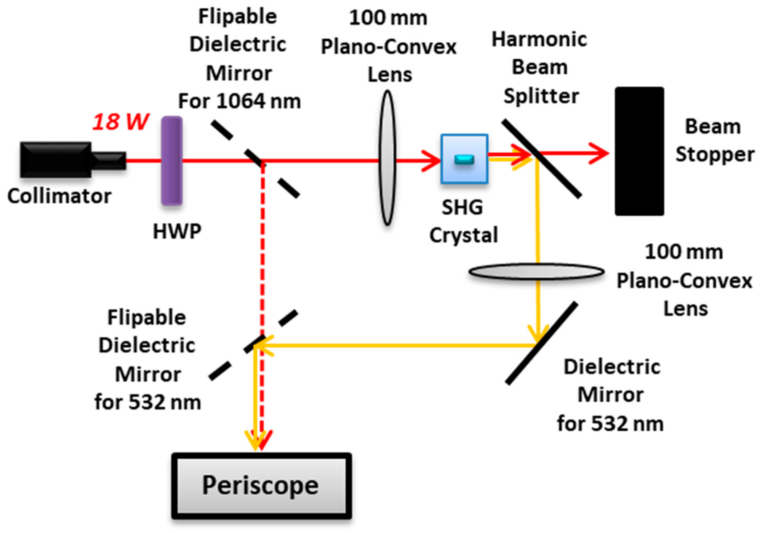
Crystalline Si has an optical band-gap of 1.12 eV corresponding to a wavelength of ~1100 nm, and dehydrogenated a-Si has an optical Tauc (band-to-band) bandgap of ~1.6-1.7 eV corresponding to ~750 nm. However, a-Si also has Urbach band tails and dangling bond defect states in the bandgap which effectively results in very high absorption at wavelengths >750 nm [
19]. The optical absorption in a-Si thin film can be achieved by wavelengths <1100 nm means that irradiation at both wavelengths of 1064 nm and 532 nm has the potential for LC process. Therefore, an SHG line is designed in order to construct an optical system which allows users to choose the wavelength by using a flip mirror [
4,
11,
12]. A dielectric flip mirror for 1064 nm is used after the collimator to interchange the LC process irradiation wavelength. The 1064 nm laser beam is directed to two different paths according to the position of the flip mirror. One path is aligned to a periscope and the other one continues to an SHG crystal [
20,
21,
22,
23,
24,
25,
26,
27,
28]. Before the flip mirror, a half wave plate (HWP) is used to rotate the polarization orientation of the incoming beams of the laser system. For SHG, an f = 100 mm lens is used to focus the fundamental beam inside a type-1 lithium triborate crystal (LiB
3O
5 -LBO) crystal with dimensions of 3 mm × 3 mm × 20 mm [
21,
22,
23,
24,
25,
26,
27]. The optical spectrum is limited by the phase-matching bandwidth of 1 nm for LBO at ~1064 nm [
21,
29,
30]. The optimum phase matching is achieved at 152.5 °C [
28]. Input and output surfaces of the crystal have anti-reflection coatings for the wavelengths of 1064 nm and 532 nm. Two different beams are expected in the output of SHG crystal because of the nature of frequency doubling [
21,
22,
23,
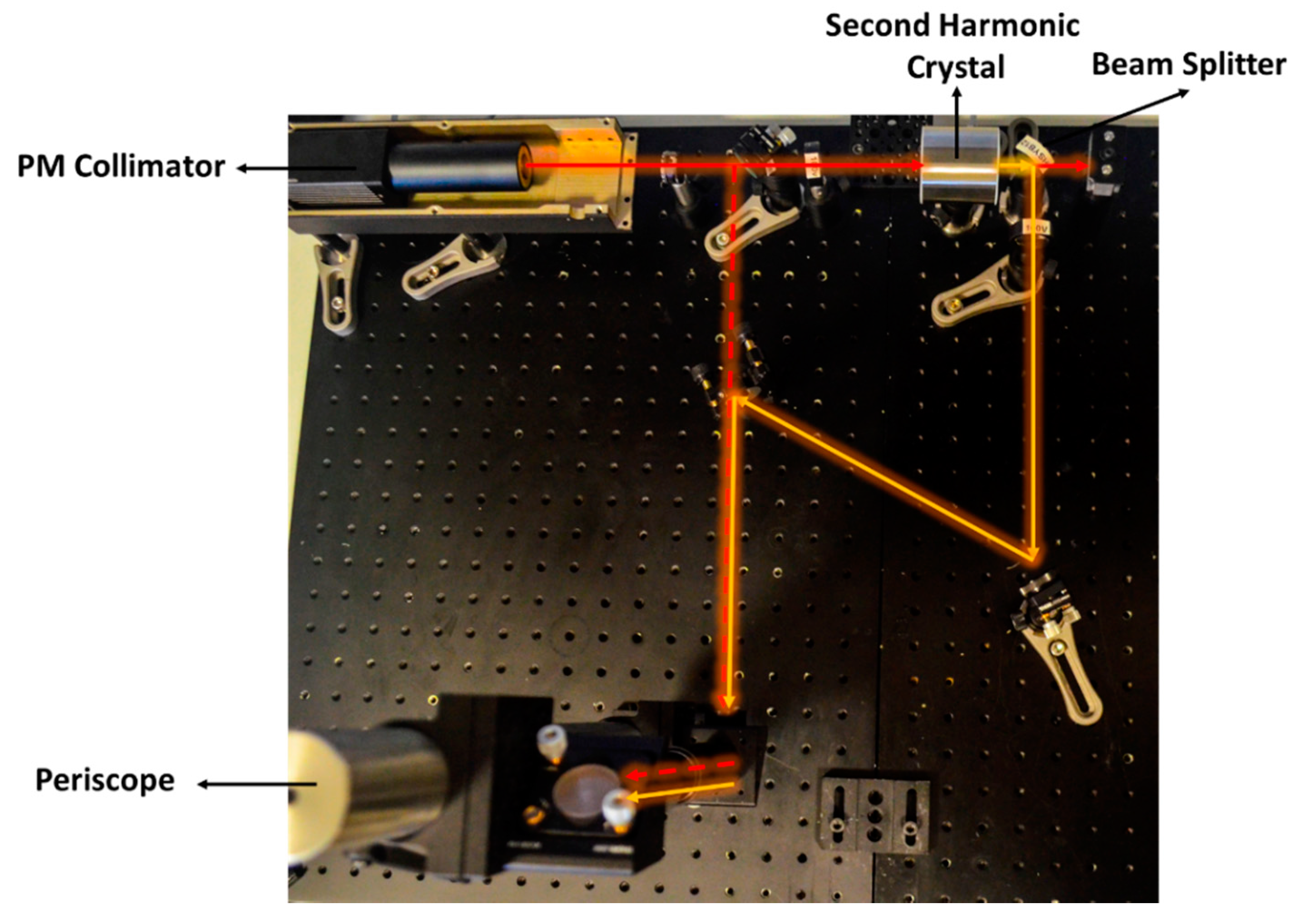
24]. After SHG, a harmonic beam splitter which reflects 532 nm and transmits the residual wavelengths is used to separate the residual fundamental radiation coming out from SHG process. An f = 100 mm lens is used to re-collimate the light. In the end, an additional flip mirror guides the frequency doubled beam to the periscope. The fundamental and frequency doubled beams are aligned collinearly and directed towards the periscope. The SHG stage layout and the corresponding photograph are shown in
Figure 9 and
Figure 10, respectively.
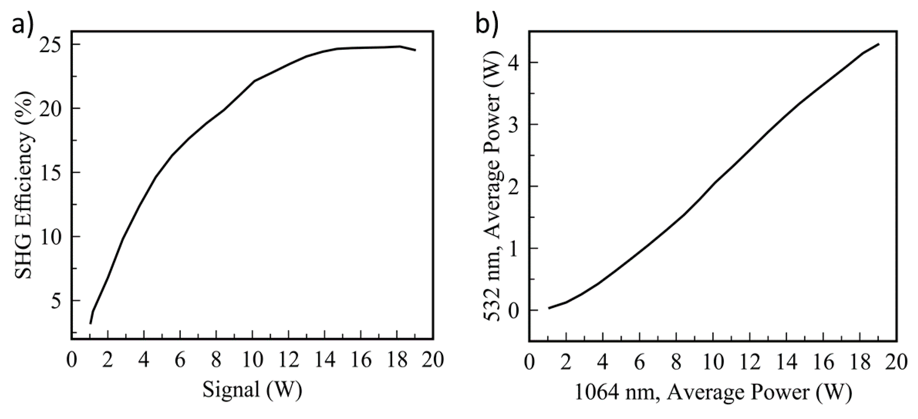
An efficiency of 25% is achieved in conversion of 1064 nm to 532 nm as shown in
Figure 11a and b, respectively.
The operation parameters belonging to 1064 nm and 532 nm lines are summarised in
Table 1.
2.3. Materials Processing Platform
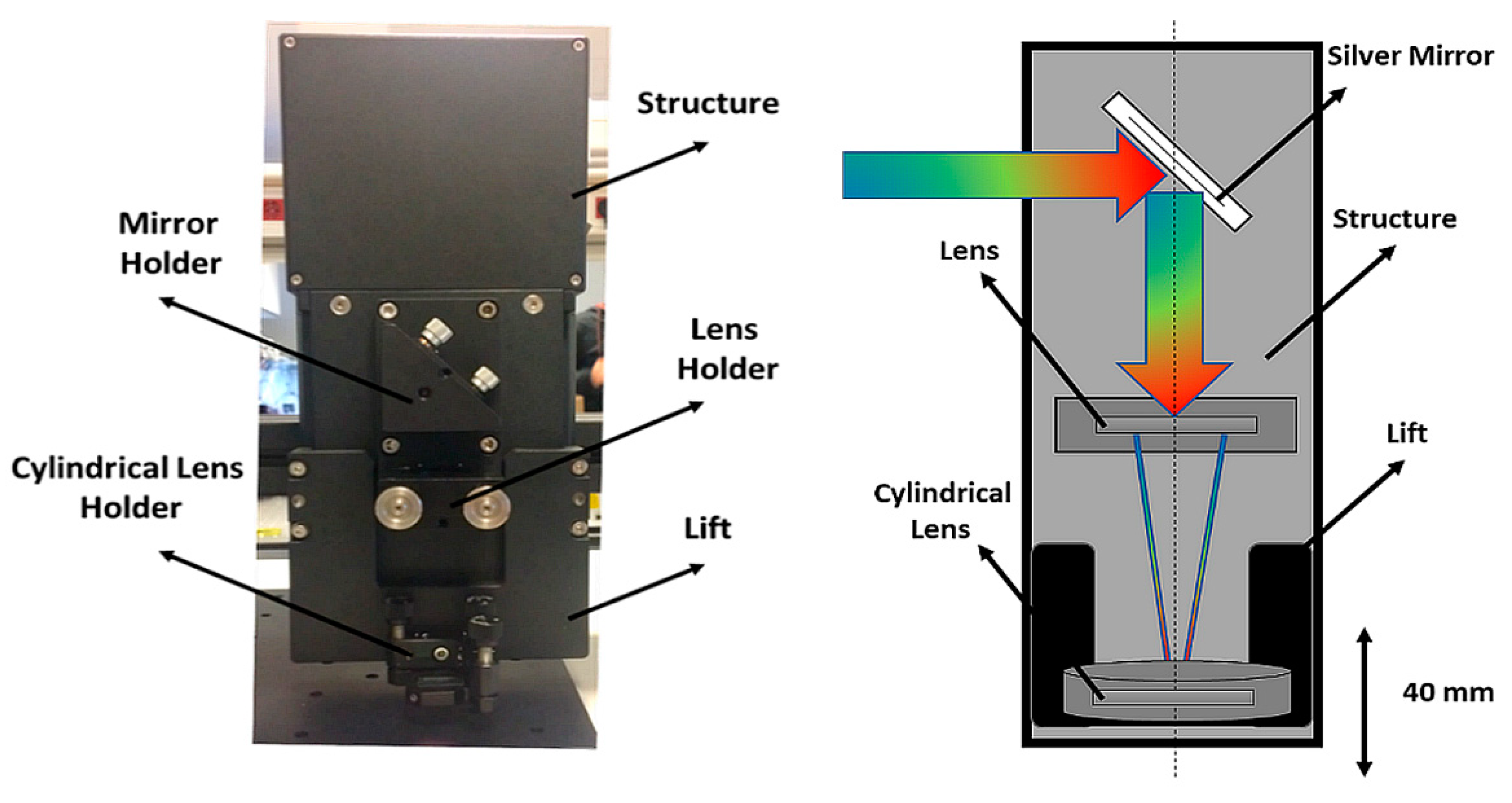
The last stage of the setup contains a motorized platform with an optical circuit generating a line-focus on the sample surface. The fundamental and SHG lines are aligned collinearly throughout the optical setup. It consists of kinematic mounts for a round mirror, a plano-convex lens, a cylindrical lens and a lift. All the optomechanical components and optics are fixed on the structure as shown in
Figure 12.
Kinematic mounts are used to hold optics and provide ±4° two axes tip and tilt adjustments. With these kinematic abilities, the incoming beam can easily be aligned throughout the setup with sufficient degrees of freedom. Distance between the cylindrical lens and the plano-convex lens is important in adjusting the length of line-focus on sample surface, so a lift is employed to provide capability of adjusting the distance between the cylindrical lens and the platform surface. Checking beam diameter and focal length of lenses at entrance of the setup is crucial for attaining a desired length of the line-focus. Moreover, the focal length of the plano-convex lens at 1064 nm and 532 nm are different due to dispersion. Another reason why a lift for the cylindrical lens is added to the structure is that fine adjustment of the focus size can thereby be performed. The layout of the line-focus setup is given in
Figure 13. The calculation of the line-focus length is given in Equation (1).
In Equation (1), L is the length of the line-focus at the focal point of plano-convex lens, y is the distance of the cylindrical lens from the surface where the focal point of plano-convex lens is fixed on the surface of the sample, D is the diameter of the beam and
Fc,
Fθ are the focal distances of the plano-convex and the cylindrical lenses, respectively [
31]. The width of the minor axis is measured to be approximately 45 µm and it is above the diffraction limit.
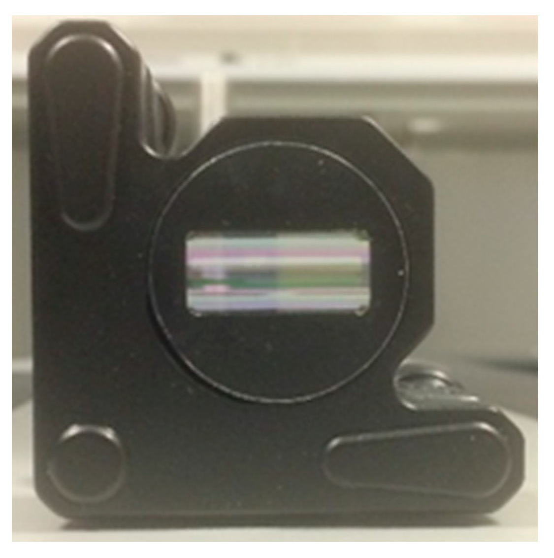
The holder of the cylindrical lens is designed with respect to the dimensions of cylindrical lens and placed in a kinematic mount. The lens holder is shown in
Figure 14. In addition, the kinematic mount has mounting screws at its own edges to orient the axis of the cylindrical lens perpendicularly with respect to the incoming beam as shown in
Figure 15. The two alternative mounting orientations of the cylindrical lens allows the successive pulses to form overlapping marks of the line-focus on the sample surface in a longitudinal or latitudinal manner. In other words, major and minor axes’ lengths of the line-focus can be interchanged easily without changing the scanning axes of the motorized sample scanner.
In order to keep the optical circuit (c in
Figure 16) above a large range sample scanner (b in
Figure 16), a sturdy bridge (d in
Figure 16) is constructed on a platform table (a in
Figure 16).
The step motorized scanner needs to stay on a vibration-isolated uniform planar surface, so it is mounted on a rigid table. In addition, the four table supports are tied together by horizontal bars for extra rigidity. The motorized scanner has a 350 mm × 350 mm processing area and it has a positional resolution of <0.2 µm. Its speed can be varied between 1–100 mm/s and positional repeatability is below 5 µm. In order to control the laser system and the motorized scanner simultaneously, a software user interface is also necessary. The user interface allows the movements of the motorized scanner to be controlled synchronously by modulating on/off times of the fibre-laser. Besides, user controls parameters such as pulse width and repetition rate through the user interface. The motion controls, such as acceleration, deceleration, and speed are also controlled through the user interface. By these software controls, unwanted vibrations due to large momentum of the scanner can be minimized as much as possible in fast movements.
2.4. Demonstration
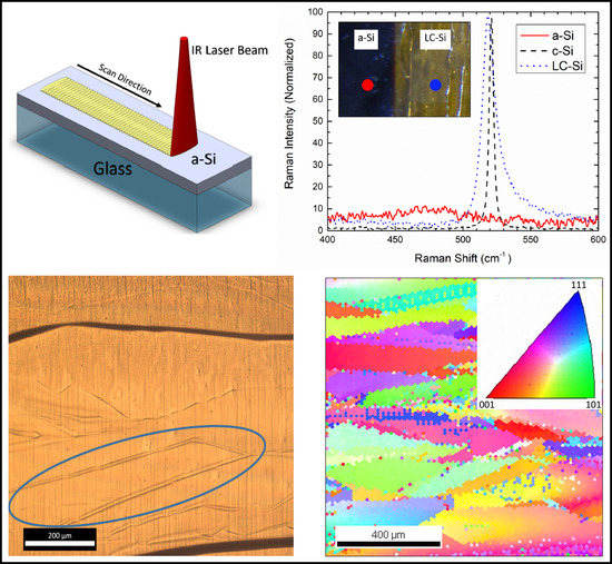
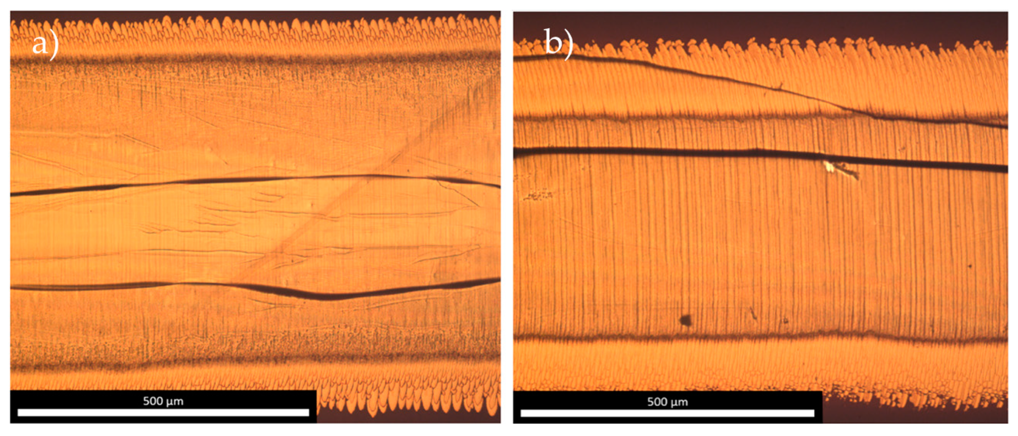
A 1 µm thick intrinsic a-Si film was deposited on a 1.1 mm thick solar glass substrate by e-beam evaporation method. Two different regions of the same sample were scanned by the fundamental line at 1064 nm and the SHG line separately at room temperature. The sizes of the line-focus were adjusted to form an elliptical shape with a major axis of 1000 µm and a minor axis of 45 µm length for both wavelengths. The repetition rate of pulses and the pulse duration were fixed at values of 200 kHz and 16 ns, respectively. For the LC process with 1064 nm, the optimum pc-Si formation was achieved with a pulse energy of 43 μJ and pulse overlap of 99.82% (see
Figure 17a). An optimum LC process with 532 nm was determined to be with a pulse energy of 16 μJ and a pulse overlap of 99.93% (see
Figure 17b).
The scan direction was from left to right in both
Figure 17a,b. The scan speeds were 16 mm/s and 6 mm/s for 1064 nm and 532 nm, respectively. At a first glance, the LC process by 1064 nm exhibited more homogeneous and directional growth of crystalline domains than that of the 532 nm. In
Figure 17b, successive vertical lines formed by surface shockwaves of explosive crystallization (EC) [
4,
32,
33] can be clearly observed. The dark regions located at the top and bottom and the bottom of
Figure 17a,b are unprocessed a-Si regions. Several bold dark horizontal features throughout scanned regions can be seen in both figures. These are confirmed to be deformations of the substrate surface at the film–substrate interface and the deformations do not reach the film surface (confirmed by atomic force microscopy, not shown). The deeper penetration of 1064 nm initiates a-Si to melt starting from the substrate interface with the film. This causes more homogenously formed crystalline domains with respect to 532 nm LC process.
Figure 18 shows a zoomed region of sample in
Figure 17a.
In the microscope image of
Figure 18, a pc-Si domain is noticeable under the optical microscope. However, this type distinctive domain formation features are not distinguishable in the sample shown in
Figure 17b, which was LC processed by 532 nm irradiation.
3. Results
Our pulsed laser processing platform providing 18 W of average power at 1064 nm converts with a 25% efficiency, yielding an average power of 4 W, to 532 nm via its SHG stage. Throughout our demonstrations, the crystallization was performed at constant sample scan speed. In our demonstrations we have optimized operation parameters for LC process by Raman spectroscopy and EBSD measurements.
Figure 19 shows Raman spectra of the LC processed regions that are shown in
Figure 17a,b. The spectra were compared with reference intrinsic bulk c-Si and non-processed regions of the a-Si film. The Raman spectra show that the LC process by both fundamental and SHG laser lines successfully induced crystallization with peak positions comparable to the reference bulk c-Si. The FWHM of both LC processes are larger than c-Si reference due to the resulting films’ polycrystalline nature.
The crystalline domain formation indicated by the microscope images as in
Figure 18 were confirmed by EBSD analyses.
Figure 20 shows an EBSD image of an LC processed region performed at 1064 nm.
The EBSD analyses showed that crystalline domains grow in the direction of the sample scan which is perpendicular to the long axis of the line-focus. The length of individual crystalline domains reaches up to several millimetres.
4. Discussion
As a general rule, short nonlinear crystals are preferred for SHG with ultrafast pulses, because excessively high peak powers of femtosecond pulses cause conversion efficiency to decrease drastically in long crystals. Moreover, femtosecond pulses disperse significantly when they are allowed to propagate in a nonlinear crystal [
29]. These effects occurring at the femtosecond regime have a negative influence on harmonic generation. However, dispersion of nanosecond pulses can be negligible when compared to femtosecond pulses in longer crystals. For that reason, in our nanosecond pulsed laser platform, long nonlinear crystals (in our case, 3 mm × 3 mm × 20 mm) could safely be utilised in harmonic generation. Nevertheless, spectral linewidth of the fundamental laser line should be sufficiently narrow for efficient harmonic conversion in a long nonlinear crystal. Since the phase-matching bandwidth of the type-1 LBO crystal is 1 nm at 1064 nm [
21,
29,
30], we paid special attention to keep the spectral linewidth of the fundamental line as narrow as possible.
It was observed that the passive fibre after the gain amplifiers caused nonlinear optical effects for peak powers exceeding 1 kW. This caused broadening in the optical spectrum of the signal and the conversion efficiency of SHG started to decrease in the crystal. Consequently, the length of the passive fibre before the collimator (after gain fibre of final-amplifier) was shortened as much as possible. However, the nonlinear effects could not be prevented completely. The highest conversion efficiency for SHG was achieved with a repetition rate of 200 kHz and a pulse duration of 16 ns where the average power was 18 W at 1064 nm. Using these parameters, the spectral linewidth of the fundamental line was maintained at 2 nm. The SHG conversion efficiency was limited to 25% in our all-fibre configuration. It can be increased by using free-space optical components. A free-space optical isolator and a free-space MPC design can be employed to decrease nonlinear effects. However, it should be noted that a higher SHG pulse energy can be achieved with a free-space design at the cost of robustness and compactness which is offered by the all-fibre design. Wavelength drift due to thermal build-up at the diodes was eliminated successfully by using TEC based wavelength stabilized diodes in amplifiers. With help of these diodes, the optical spectrum of pump signal was kept stable.
5. Conclusions
In this paper, a multi-wavelength laser processing platform design, its construction, and its successful demonstration are reported in laser crystallization of a-Si thin films. The design is based on ytterbium doped MOPA fibre laser operating at 1064 nm. The repetition rate, the average power, the pulse width and the LC process scan speed are determined to lie between lower and upper limits of 80 kHz–300 kHz, 1 W–18 W, 15 ns–40 ns, 1 mm/s–100 mm/s, respectively. By help of polarization maintaining fibre-optical components, the beam was kept at linear polarization with an extinction ratio of 1:450. An SHG stage was built and integrated to the fibre laser platform. A 25% conversion efficiency was achieved. A 2-axis materials processing stage was built and integrated with the laser system. This motorized process stage has a 350 mm × 350 mm area and a positional resolution of <0.2 µm. It is supported on a vibration-isolated table. The motorized stage is controlled synchronously with the laser system through modulation of the laser pulse duty cycle. Through a free-space optical setup, the SHG and fundamental beams were line-focused onto samples. In addition, a software user interface was developed to control diverse parameters of the laser and the motorized sample scanner.
The multi-wavelength laser crystallization platform operation in LC of Si thin films at both wavelengths of 1064 nm and 532 nm was successfully demonstrated. It was possible to maintain LC of 1 µm thick a-Si film without creating damage on the formed crystalline surfaces and the glass substrates using both wavelengths. The LCs of Si thin films were verified quantitatively by means of Raman and EBSD analyses. Rotating the long axis of the line-focus orthogonally, or using successive non-overlapping pulses, provides the means to pattern crystalline regions for fabrication of microscopically structured devices, such as TFTs and solar cells.
We plan in the near future to implement third harmonic generation (at a wavelength of 355 nm) in this platform as an additional process wavelength in order to extend its capabilities. This can be achieved by sufficient suppression of the unwanted nonlinear effects. For this, we plan on a free space isolator collimator, and backwards pumping scheme. In addition, we plan to improve the line-focus intensity uniformity by switching from the cylindrical lens to a Powell lens.
Author Contributions
Conceptualization, A.B.; Data curation, V.T., M.E.Y., S.H.S. and K.Ç.; Formal analysis, V.T. and K.Ç.; Funding acquisition, S.K.E. and A.B.; Investigation, V.T., M.E.Y. and K.Ç.; Methodology, V.T., M.E.Y. and S.H.S.; Project administration, A.B.; Resources, S.K.E. and A.B.; Software, V.T.; Supervision, S.K.E. and A.B.; Validation, V.T., M.E.Y. and K.Ç.; Writing—original draft, V.T.; Writing—review & editing, V.T., K.Ç. and A.B.
Funding
This research was funded by TÜBİTAK under grant number 115M061.
Acknowledgments
We thank METU Central Laboratories for the EBSD acquisition. We thank Ihor Pavlov for the suggestions which led to improvements at various places.
Conflicts of Interest
The authors declare no conflict of interest. The funders had no role in the design of the study; in the collection, analyses, or interpretation of data; in the writing of the manuscript, or in the decision to publish the results.
References
- Shah, A.; Torres, P.; Tscharner, R.; Wyrsch, N.; Keppner, H. Photovoltaic technology: The case for thin-film solar cells. Science 1999, 285, 692–698. [Google Scholar] [CrossRef] [PubMed]
- Green, M.A. Third generation photovoltaics: Ultra-high conversion efficiency at low cost. Prog. Photovolt. Res. Appl. 2001, 9, 123–135. [Google Scholar] [CrossRef]
- Çınar, K.; Karaman, M.; Bek, A. Improvement of laser-crystallized silicon film quality via intermediate dielectric layers on a glass substrate. ACS Omega 2018, 3, 5846–5852. [Google Scholar] [CrossRef]
- Salman, H.S.; Bacıoğlu, A.; Eken, S.K. Crystallization of Hydrogenated Amorphous Silicon Thin Film on Glass by Using NS-Pulsed Fiber Laser Operating at 1064 nm. Master’s Thesis, University of Hacettepe, Ankara, Turkey, 2019. [Google Scholar]
- Dore, J.; Evans, R.; Schubert, U.; Eggleston, B.D.; Ong, D.; Kim, K.; Huang, J.; Kunz, O.; Keevers, M.; Egan, R.; et al. Thin-film polycrystalline silicon solar cells formed by diode laser crystallization. Prog. Photovolt. Res. Appl. 2013, 21, 1377–1383. [Google Scholar] [CrossRef]
- Sonntag, P.; Haschke, J.; Kuhnapfel, S.; Gabriel, O.; Amkreutz, D.; Rech, B. Properties of liquid phase crystallized interdigitated backcontact solar cells on glass. Energy Procedia 2015, 77, 487–492. [Google Scholar] [CrossRef][Green Version]
- Pakhuruddin, M.Z.; Huang, J.; Dore, J.; Varlamov, S. Light Absorption Enhancement in Laser-Crystallized Silicon Thin Films on Textured Glass. IEEE Photovolt. 2016, 6, 852–859. [Google Scholar] [CrossRef]
- Varlamov, S. Polycrystalline silicon on glass thin-film solar cells: A transition from solid-phase to liquid-phase crystallised silicon. Sol. Energy Mater. Sol. Cells 2013, 119, 246–255. [Google Scholar] [CrossRef]
- Kühnapfel, S.; Gall, S.; Rech, B.; Amkreutz, D. Towards monocrystalline silicon thin films grown on glass by liquid phase crystallization. Sol. Energy Mater. Sol. Cells 2015, 128, 86–91. [Google Scholar] [CrossRef]
- Dore, J.; Ong, D.; Varlamov, S.; Egan, R.; Green, M.A. Progress in Laser-Crystallized Thin-Film Polycrystalline Silicon Solar Cells: Intermediate Layers, Light Trapping, and Metallization. IEEE Photovolt. 2014, 4, 33–39. [Google Scholar] [CrossRef]
- Taheri, M.L.; McGowan, S.; Nikolova, L.; Evans, J.E.; Teslich, N.; Lu, J.P.; LaGrange, T.; Rosei, F.; Siwich, B.J.; Browning, N.D. In situ laser crystallization of amorphous silicon: Controlled nanosecond studies in the dynamic transmission electron microscope. Appl. Phys. Lett. 2010, 97, 032102. [Google Scholar] [CrossRef]
- Weizman, M.; Rhein, H.; Dore, J.; Gall, S.; Klimm, C.; Andra, G.; Schultz, C.; Fink, F.; Rau, B.; Schlatmann, R. Efficiency and stability enhancement of laser-crystallized polycrystalline silicon thin-film solar cells by laser firing of the absorber contacts. Sol. Energy Mater. Sol. Cells 2014, 120, 521–525. [Google Scholar] [CrossRef]
- Green, M.A.; Basore, P.A.; Chang, N.; Clugston, D.; Egan, R.; Evans, R.; Hogg, D.; Jarnason, S.; Keevers, M.; Lasswell, P.; et al. Crystalline silicon on glass (CSG) thin–film solar cell modules. Sol. Energy 2004, 77, 857–863. [Google Scholar] [CrossRef]
- Liu, M.; Chen, S.; Zhang, B.M.; Li, X.; Shum, P.P.; Wang, Q.; Cheng, X. Pulse Shape Tuning for 1064 nm Nanosecond MOPA Fibre Laser. Procedia Eng. 2016, 140, 123–126. [Google Scholar] [CrossRef][Green Version]
- Zervas, M.N.; Codemard, C.A. High Power Fiber Lasers: A Review. IEEE J. Sel. Top. Quantum Electron. 2014, 20, 219–241. [Google Scholar] [CrossRef]
- Aydın, Y.O. Development of A 60 W Pulsed Fiber Laser Amplifier for Materials Processing. Master’s Thesis, Middle East Technical University, Ankara, Turkey, 2014. [Google Scholar]
- Paschotta, R.; Nilsson, J.; Anne, C.T.; David, C.H. Ytterbium-Doped Fiber Amplifiers. IEEE J. Sel. Top. Quantum Electron. 1997, 33, 1049–1056. [Google Scholar] [CrossRef]
- Limpert, J.; Röser, F.; Schreiber, T.; Tünnermann, A. High-power ultrafast fiber laser systems. IEEE J. Sel. Top. Quantum Electron. 2006, 12, 233–244. [Google Scholar] [CrossRef]
- Joannopoulos, J.D.; Lucovsky, G. The Physics of Hydrogenated Amorphous Silicon II—Electronic and Vibrational Properties; Springer: Berlin, Germany, 1984; Volume 56, pp. 154–196. [Google Scholar]
- Shanon, Z.S.; Alnayli, R.S.; Tahir, K.J. Study of the Second and Third Harmonics Generation in Lithium Tribrate Single Crystal. Int. J. Sci. Res. 2016, 5, 1614–1618. [Google Scholar]
- Sukhoy, K. Generation of Green Second Harmonic Radiation in LBO, BiBO, KTP, and PPLN Crystals Using Passively Q-Switched Sub-Nanosecond Microchip Laser. Master’s Thesis, University of Manitoba, Winnipeg, MB, Canada, 2011. [Google Scholar]
- Lin, S.; Sun, Z.; Wu, B.; Chen, C. The nonlinear optical characteristics of a LiB3O5 crystal. J. Appl. Phys. 1990, 67, 634–638. [Google Scholar] [CrossRef]
- Arne, P. Nonlinear Optical Frequency Conversion for Lasers in Space. Diplom Thesis, University of Tübingen, Tübingen, Germany, 2014. [Google Scholar]
- Nikogosyan, D.N. Lithium triborate (LBO)—A review of its properties and applications. Appl. Phys. A 1994, 58, 181–190. [Google Scholar] [CrossRef]
- Zhang, J.; Huang, J.Y.; Wang, H.; Wong, K.S.; Wong, G.K. Second-harmonic generation from regeneratively amplified femtosecond laser pulses in BBO and LBO crystals. Opt. Soc. Am. B 1998, 15, 200–209. [Google Scholar] [CrossRef]
- Favre, S.; Thomas, C.S.; Rene, P.S. High-Power Long-Pulse Second Harmonic Generation and Optical Damage with Free-Running Nd: YAG Laser. IEEE J. Sel. Top. Quantum Electron. 2003, 39, 733–740. [Google Scholar] [CrossRef]
- Gontijo, I. Determination of important parameters for second harmonic generation in LBO. Opt. Commun. 1994, 108, 324–328. [Google Scholar] [CrossRef]
- Thyagarajan, K.; Ghatak, A.K. Fiber and guided wave optics: nonlinear optics. In Encyclopedia of Modern Optics; Guenther, R.D., Ed.; Elsevier: Amsterdam, The Netherlands, 2005; Volume 1, pp. 472–486. [Google Scholar]
- Hussain, K.; Kumbhakar, P. Nonlinear optical properties of some newly developed crystals for measurement of ultrafast laser pulses. Braz. J. Phys. 2006, 36, 1281–1284. [Google Scholar] [CrossRef]
- Khanh, K.; Brian, G.S.; Gary, R.H.; Sunney, X.; Frank, W.W. High-power picosecond fiber source for coherent Raman microscopy. Opt. Lett. 2009, 34, 2051–2053. [Google Scholar]
- Çınar, K. Nanosecond Pulsed Infrared Laser Induced Crystallization of Amorphous Silicon Films for Potential Photovoltaic Applications. Ph.D. Thesis, Middle East Technical University, Ankara, Turkey, 2018. [Google Scholar]
- Jin, J.; Yuan, Z.; Huang, L.; Chen, S.; Shi, W.; Cao, Z.; Lou, Q. Laser crystallization of amorphous silicon thin films investigated by Raman spectroscopy and atomic force microscopy. Appl. Surf. Sci. 2010, 256, 3453–3458. [Google Scholar] [CrossRef]
- Andra, G.; Bergmann, J.; Falk, F. Laser crystallized multicrystal-line silicon thin films on glass. Thin Solid Films 2005, 487, 77–80. [Google Scholar] [CrossRef]
Figure 1.
Overview of the thin film a-Si crystallization laser platform.
Figure 1.
Overview of the thin film a-Si crystallization laser platform.
Figure 2.
(a) Pulse width and (b) repetition rate of seed diode.
Figure 2.
(a) Pulse width and (b) repetition rate of seed diode.
Figure 3.
Optical spectrum of the seed diode.
Figure 3.
Optical spectrum of the seed diode.
Figure 4.
The laser pre-amplifier layout.
Figure 4.
The laser pre-amplifier layout.
Figure 5.
Optical spectrum (a) after the middle-amplifier, (b) after the final-amplifier.
Figure 5.
Optical spectrum (a) after the middle-amplifier, (b) after the final-amplifier.
Figure 6.
Pump-signal conversion efficiency at the output of the fibre laser.
Figure 6.
Pump-signal conversion efficiency at the output of the fibre laser.
Figure 7.
The middle- and final-amplifier layout.
Figure 7.
The middle- and final-amplifier layout.
Figure 8.
Photograph of the unboxed laser system on an optical table.
Figure 8.
Photograph of the unboxed laser system on an optical table.
Figure 9.
Layout of the second harmonic generation (SHG) section.
Figure 9.
Layout of the second harmonic generation (SHG) section.
Figure 10.
Photograph of the SHG section.
Figure 10.
Photograph of the SHG section.
Figure 11.
(a) Conversion efficiency and (b) average power of SHG.
Figure 11.
(a) Conversion efficiency and (b) average power of SHG.
Figure 12.
Photograph (left) and layout (right) of the optical circuit for line-focusing.
Figure 12.
Photograph (left) and layout (right) of the optical circuit for line-focusing.
Figure 13.
Layout of the line-focus setup.
Figure 13.
Layout of the line-focus setup.
Figure 14.
Cylindrical lens holder.
Figure 14.
Cylindrical lens holder.
Figure 15.
Orientations of kinematic mount for cylindrical lens.
Figure 15.
Orientations of kinematic mount for cylindrical lens.
Figure 16.
Materials processing platform: (a) platform table, (b) motorized sample scanner, (c) optical circuit, (d) bridge.
Figure 16.
Materials processing platform: (a) platform table, (b) motorized sample scanner, (c) optical circuit, (d) bridge.
Figure 17.
Top view optical microscope image of the laser crystallization (LC) processed regions by (a) 1064 nm (b) 532 nm. The transverse line focus is scanned horizontally parallel to the scale bar. Darker top and bottom edges are unprocessed regions.
Figure 17.
Top view optical microscope image of the laser crystallization (LC) processed regions by (a) 1064 nm (b) 532 nm. The transverse line focus is scanned horizontally parallel to the scale bar. Darker top and bottom edges are unprocessed regions.
Figure 18.
LC of a-Si by 1064 nm. (See figure caption 17 for further details.).
Figure 18.
LC of a-Si by 1064 nm. (See figure caption 17 for further details.).
Figure 19.
Raman spectra of 1064 nm and 532 nm LC processed regions with c-Si and a-Si references.
Figure 19.
Raman spectra of 1064 nm and 532 nm LC processed regions with c-Si and a-Si references.
Figure 20.
Electron back scattered diffraction (EBSD) of an LC region processed at 1064 nm.
Figure 20.
Electron back scattered diffraction (EBSD) of an LC region processed at 1064 nm.
Table 1.
Parameters of fundamental and SHG laser lines.
Table 1.
Parameters of fundamental and SHG laser lines.
| Wavelength (nm) | Average
Power
(W) | Repetition
Rate
(kHz) | Pulse
Width
(ns) | Pulse
Intensity
(µJ) | Peak
Power
(kW) | Polarization | Beam
Quality (M2) |
|---|
| 1064 ± 1 | 18 ± 0.5 | 80–300 | 15–40 | 225–60 | 15–1.5 | Linear | 1.2 |
| 532 | 4 ± 0.1 | 200 | 15–17 | 20 | 1.25 ± 0.8 | Linear | <1.5 |
© 2019 by the authors. Licensee MDPI, Basel, Switzerland. This article is an open access article distributed under the terms and conditions of the Creative Commons Attribution (CC BY) license (http://creativecommons.org/licenses/by/4.0/).

 ,
, 


