Article

X-Rays Writing/Reading of Charge Density Waves in the CuO2 Plane of a Simple Cuprate Superconductor

1
Institute of Crystallography, CNR, Monterotondo, 00015 Roma, Italy
2
Deutsches Elektronen-Synchrotron DESY, 22607 Hamburg, Germany
3
Department of Physics, Harvard University, Cambridge, MA 02138, USA
4
Fondazione Santa Lucia I.R.C.C.S., 00179 Roma, Italy
5
Rome International Center of Materials Science (RICMASS), 00185 Roma, Italy
*
Author to whom correspondence should be addressed.
Condens. Matter 2017, 2(3), 26; https://doi.org/10.3390/condmat2030026
Submission received: 4 July 2017 / Revised: 2 August 2017 / Accepted: 8 August 2017 / Published: 11 August 2017

Abstract

:
It is now well established that superconductivity in cuprates competes with charge modulations giving an electronic phase separation at nanoscale. More specifically, superconducting electronic current takes root in the available free space left by electronic charge ordered domains, called charge density wave (CDW) puddles. This means that CDW domain arrangement plays a fundamental role in the mechanism of high temperature superconductivity in cuprates. Here we report about the possibility of controlling the population and spatial organization of the charge density wave puddles in a single crystal La2CuO4+y through X-ray illumination and thermal treatments. We apply a pump-probe method—based on X-ray illumination as a pump and X-ray diffraction as a probe—setting a writing/reading procedure of CDW puddles. Our findings are expected to allow new routes for advanced design and manipulation of superconducting pathways in new electronics.

Graphical Abstract

1. Introduction

The nano-electronics for new generations of devices made of complex modern materials are extremely sensitive to changes in defect disposition [1,2,3]. To control defect complexity in superconductors, some experimental approaches have been proposed. The manipulation of an array of superconducting grains has been found to be possible by either controlling defects self-organization using scanning tips [4] or using external stimulus [5,6,7,8,9]. Recently, the improvement of film deposition techniques has allowed the production of artificial superconducting puddles embedded in a 2D layer intercalated by different block layers in a layered material [10,11,12,13]. Although it is common knowledge that a suspended two-dimensional layer should be thermodynamically unstable, and therefore should not exist in nature [14], new advanced materials such as two-dimensional graphene have recently challenged this paradigm [15,16,17]. In this material, electronic properties are affected by curved geometries originating from topological defects such as dislocations or ripples.
High temperature superconductors (HTS) are hetero-structures, at their atomic limit, made of intercalated two-dimensional layers. Like graphene, CuO2 layers (with the structure of the 110 plane of a body centered cubic (bcc) lattice) in cuprates [18,19], as well as boron (B) layers in diborides [20,21,22] or FeSe layers in AxFe2−ySe2 chalcogenides [23] are truly two-dimensional crystals (just one atom thick). Because of their general instability with respect to bending fluctuations, these conductive planes are rippled and these effects are enormously relevant for their structural, thermodynamic, and electronic properties. Using strain engineering it is possible to modify in a desirable way the electronic structure of atomic layers with exciting perspectives for electronics. In case of HTS, electronic organization in modulated structures called charge density waves (CDWs) have been found to play an essential role in superconducting mechanisms [24,25,26,27]. In fact, it has been established that electronic superconducting currents develop in the space free from CDWs [28,29]. In this framework, the possibility of controlling both the population and the spatial arrangement of the CDW puddles becomes a key point to be investigated for different possible applications.
CDWs in cuprates have been found recently through the real space visualization of the 3D superlattices measured by scanning micro X-ray diffraction in different single crystals [8,9,18,23,28,29,30]. These transverse modulations are similar to those found in the superconducting Bi2212, characterized by the wave-vectors 0.21b* [31,32]. They are due to stripes with a period of 4.8b along the diagonal direction b. It has been found that the CDW puddles are spatially anti-correlated with other spin and charge ordered puddles and with domains rich with interstitial dopant oxygen defects [28,33,34,35,36] in a scenario of frustrated phase separation which is a common feature of doped cuprates [37,38,39,40,41]. Either oxygen interstitial-rich domains or CDW puddles are sensitive to X-ray illumination in a different temperature range [42,43] but together they work to establish the optimum inhomogeneity, which raises the critical temperature to the optimum value [18]. Here we study CDW puddles in an oxygen doped orthorhombic La2CuO4+y (LCO) superconductor showing the details of the manipulation process, which allow tuning of the order of the CDW puddles in the LCO system.

2. Materials and Methods

Diffraction measurements on a single crystal of underdoped La2CuO4+y of size 3 × 2 × 0.5 mm3, were performed on the crystallography beamline, XRD1, at ELETTRA, Trieste, Italy [44]. The sample was grown first as La2CuO4 by flux method and then doped by electrochemical oxidation. The X-ray beam, emitted by the wiggler source of the 2 GeV electron storage ring, was monochromatized by a Si(111) double crystal, and focused on the sample. The superconducting transitions of samples have been established using contactless single-coil inductance as described elsewhere [5,16,30]. The temperature of the crystal was monitored with an accuracy of ±1 K. We have collected the data in the reflection geometry using a charge coupled device (CCD) detector, a photon energy of 12.4 KeV (wavelength λ = 1 Å). The sample oscillation around the crystal b-axis was in a range 0 < Φ < 20°, where Φ is the angle between the direction of the photon beam and the crystal a-axis. We have investigated a portion of the reciprocal space up to 0.6 Å−1 momentum transfer, i.e., recording the diffraction spots up to the maximum indexes h = 3, k = 3, and l = 19 in the a*, b*, and c* directions of reciprocal space, respectively. Thanks to the high brilliance source, it has been possible to record a large number of weak superstructure spots around the main peaks of the average structure. Twinning of the crystal has been taken into account to index the superstructure peaks. The orthorhombic lattice parameters of single crystal were determined to be a = (5.386 ± 0.004) Å, b = (5.345 ± 0.008) Å, c = (13.205 ± 0.031) Å at room temperature. The space group of the sample is Fmmm.

3. Results

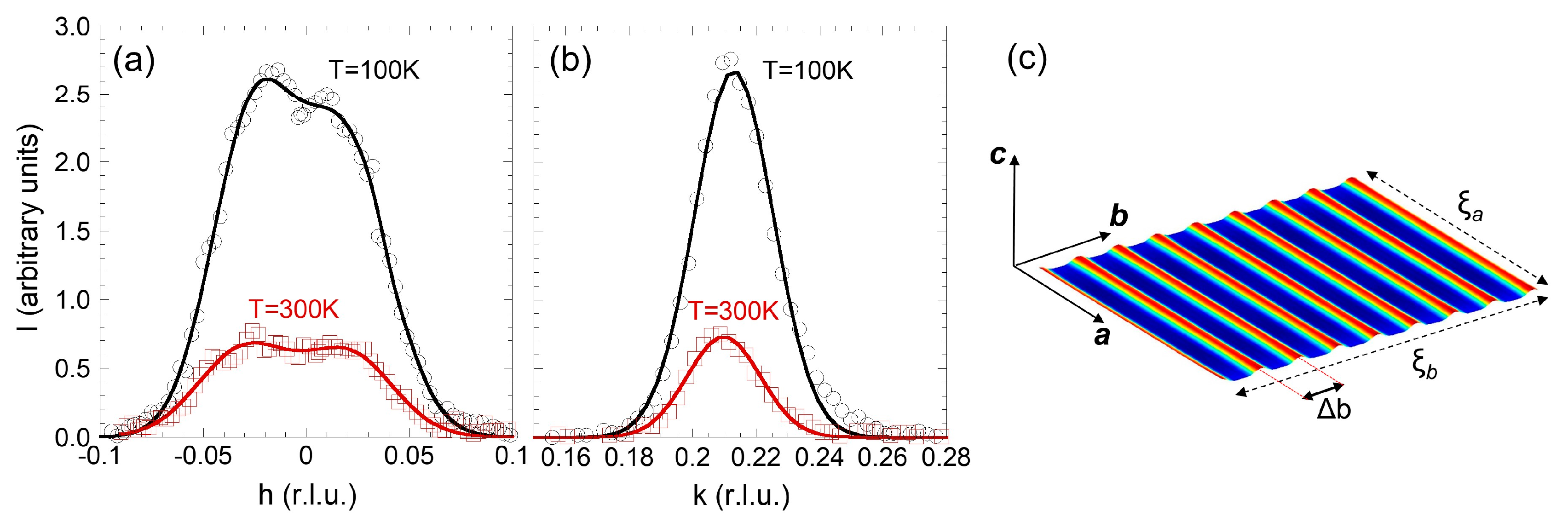
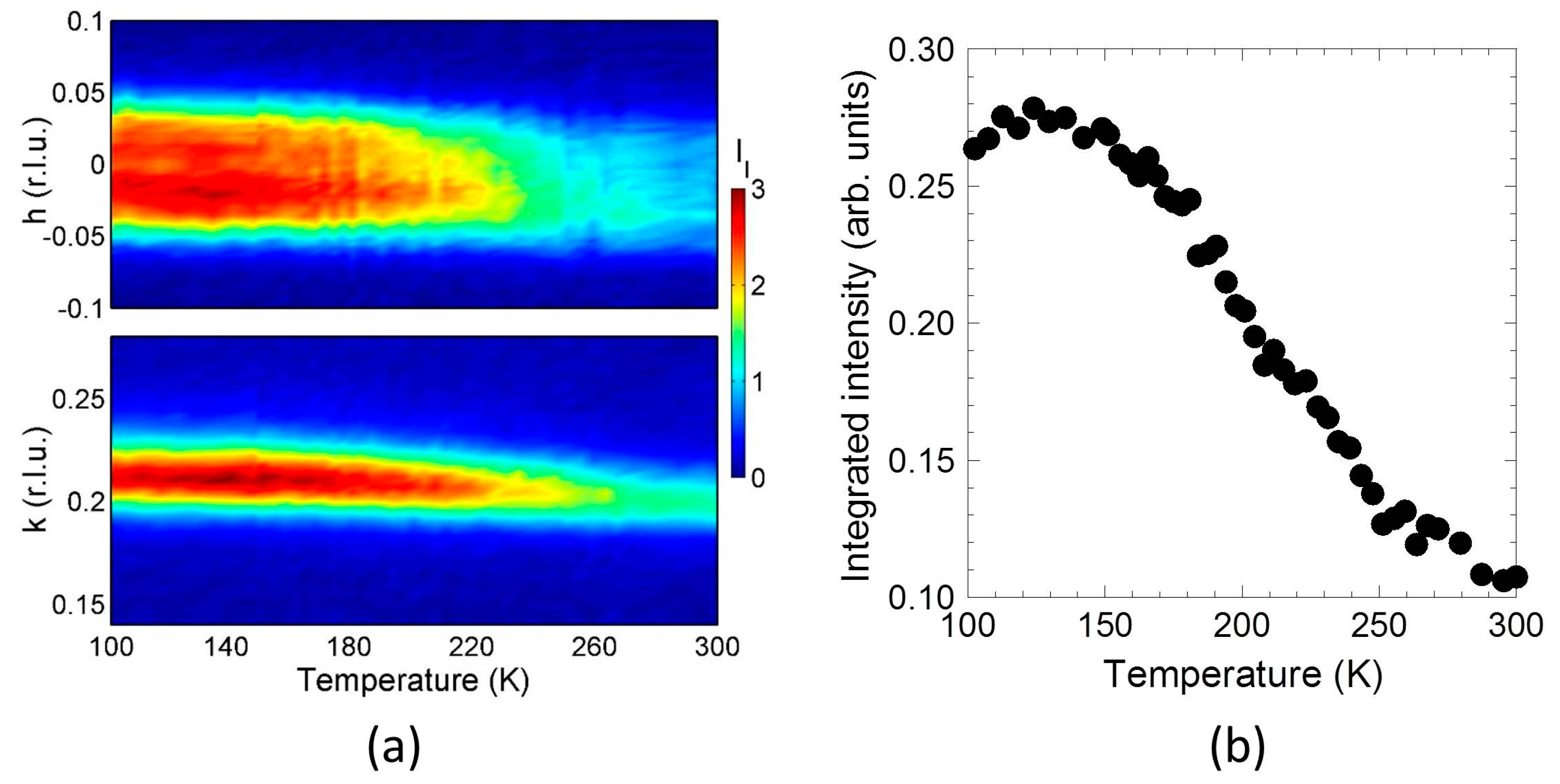
3.1. Temperature Dependence of CDW Puddles

Indexing of superlattice peaks around the Bragg lattice reflections shows the presence of incommensurate CDW modulation with wave-vector qCDW = (0.023a* + 0.21b* + 0.29c*) where a*, b*, and c* are the unit vectors of the orthorhombic reciprocal lattice. The profiles of this superstructure peak, measured at 300 K and 100 K in the a*b* plane and fitted by Gaussian line shape, are shown in Figure 1a,b.
The modulations along a* give X-ray diffuse superlattice peaks due to a quasi one-dimensional (1D) modulation associated with stripes running in the a direction with a period of about 2.6 nm in the b direction where a, and b represent the unit vectors of the orthorhombic lattice. These incommensurate charge density waves (CDWs) are established in nanoscale regions, as shown by the analysis of the widths of X-ray satellites. Indeed, the full width at half-maximum (FWHM) of the CDW peaks, along the a* and along the b* direction, are related with the correlation length of the CDW puddles ξa = a/FWHM(a*) and ξb = b/FWHM(b*). We have found 11 ± 2 nm and 19 ± 2 nm for ξa and ξb, respectively. A pictorial view of the qCDW modulation is given in Figure 1c.
The temperature dependence of the CDW order is shown in Figure 2.
The normalized profiles along the a* and b* directions are visualized by upper and lower panel in Figure 2a, respectively. The integrated intensity of the CDW peak increases by cooling the sample from room temperature down to 100 K, as shown in Figure 2b. We find a CDW onset temperature of 250 K.

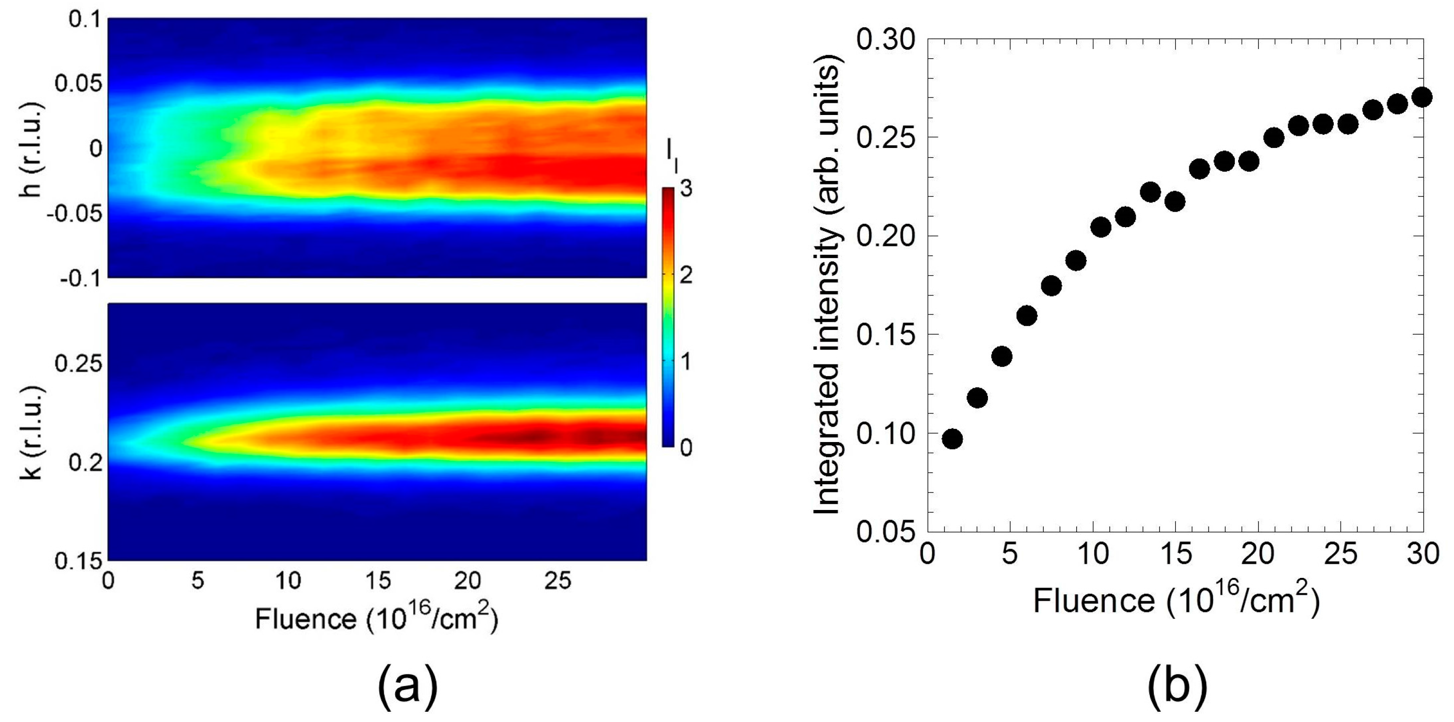
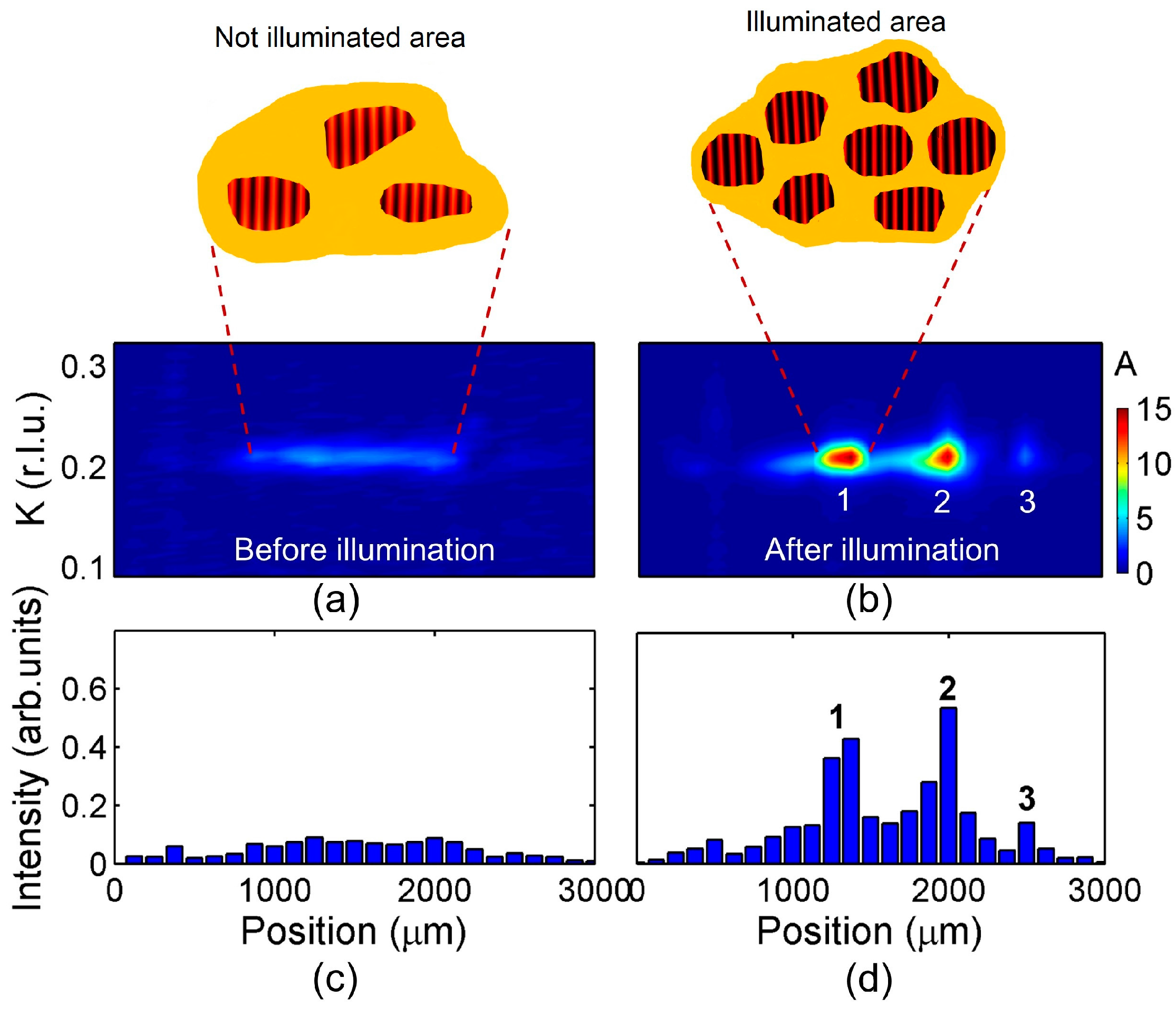
3.2. Controlling CDW Puddles by X-ray Illumination

The possibility of photo generating CDW puddles in La2CuO4+y has been previously shown in [18]. Our pump and probe experimental approach, based on X-ray illumination and diffraction, has been performed with synchrotron X-ray photons focused onto a spot size of 100 μm2 on the sample surface.
We have found that the effect of photo generation of CDW in the X-ray energy ranges between 8 KeV and 12 KeV and does not depend on photon energy but on the X-ray illumination fluence. Furthermore, new measurements are required to investigate the pump and probe process in the soft X-ray and optical regimes. The photon flux (defined as the number of photons hitting the sample surface per second per unit area) is given by ΦP(0.1nm) = 5 × 10¹⁴NP(0.1nm) s−1cm−2 and corresponds to the power density of 1 W·cm−2. In our method, the X-ray photon beam works at the same time as the pump and probe on a surface layer with an area of 100 μm2 and about 1.5 μm thick. In this volume, the physical state of the system is controlled by the fluence FP(0.1nm)(NP(0.1nm) cm−2) = ΦP·t.
We quenched the sample from room temperature, where CDW puddle population is weak, down to 100 K, leading the system to a frozen metastable disordered state. Then we illuminated the sample continuously. The pump and probe results are illustrated in Figure 3.
The color maps obtained from the normalized profiles, of qCDW(a*) and qCDW(b*) shown in the upper and lower panels of Figure 3a, respectively, visualize the evolution of CDW during the X-ray illumination. The CDW peak integrated intensity increases by about three times under illumination, as shown by the integrated intensity of qCDW peak in Figure 3b.
A single oscillation in each puddle is given by γb = b/qCDW(b*) = 2.5 nm and γa = a/ qCDW(a*) = 23.4 nm along the b and a direction, respectively; here qCDW(b*) and qCDW(a*) are the components of qCDW along the a* and b* directions. Each puddle contains a number of oscillations given by ξa/γa = 0.4 and ξb/γb = 7 in the a and b directions, respectively. Thus, we have ξa × ξb puddles made of about seven unidirectional stripes each. A pictorial view of CDW puddles is shown in the upper part of Figure 4.

3.3. CDW Writing/Reading Procedure

Thus, we have shown the feasibility of tuning the CDW population through X-ray illumination and also the possibility to erase such order by thermal treatments. These are the elementary steps for a writing/reading process. We have therefore performed a series of experiments of direct manipulation of the CDW puddles in real space in a La2CuO4+y sample through local X-ray continuous illumination at low temperatures.
Figure 4a shows the color-map of the intensity of the CDW peak, along b*, obtained by scanning the sample using an X-ray beam of 100 μm2 and a low fluence of 1.5 (1016 cm−2). The histogram in Figure 4c shows a quite flat distribution of the CDW intensity, but not zero. In fact, in order to have successful X-ray illumination growth of the CDW puddles, the region being irradiated must already have some seeds of CDW puddles, as shown by the light blue stripe in the map center of Figure 4a.
We irradiated three spots indicated by 1, 2, and 3 using an X-ray beam of 100 μm2 for a total fluence of 50 (1016 cm-2); the effects of this continuous local illumination are than monitored by re-scanning the sample using the low fluence of 1.5 (1016 cm−2). The results are shown in the map of Figure 4b by the 3 bright spots at the positions 1, 2, and 3 of increased integral intensity, respectively shown also in the histogram of Figure 4d.

4. Discussion

The relevance of the possibility of controlling and manipulating the spatial organization of CDW puddles populations lies in the fact that the free electrons form superconducting currents flowing in the interstitial space [28,29]. Thus, changing the population of the CDW puddles point by point leads to modifying the interstitial space available for the electron currents. In atomic layers, intrinsic thermodynamic instabilities give rise to charge (spin, orbital) ordering phenomena. Easy methods—such as thermal cycling and X-ray continuous illumination with focused beams—can write, read, and erase arbitrary CDW pathways. This will enable the design of new devices with controlled functionality.

5. Conclusions

In conclusion, in this paper we reported on the study of CDWs in an orthorhombic crystal La2CuO4+y where dopants are mobile oxygen interstitials. The CDWs in this compound has unique features in comparison with CDWs in different cuprate families [45,46,47,48]: the CDW wave-vector has been found to be aligned along the b orthorhombic axis in the diagonal direction from the Cu-O-Cu direction like in nikelates, cobaltates, and in the doped La124 family at very low doping. The photo-stimulated CDW puddles in La2CuO4+y are uniaxial and form a smectic phase in the crystal while in underdoped YBa2Cu3O6+y and Hg1201 form a nematic phase. Moreover, the average CDW puddles are formed by only seven oscillations which is larger than in Hg1201, but smaller than in other systems. These results support the increasing accumulating experimental evidence that the CDW character in cuprates changes in different families [45,46,47,48].
We have shown the details of the manipulation process which allow tuning of the order of the CDW puddles in the Lanthanum Copper Oxide system. This approach has unveiled the condition and the process of formation of charge density waves puddles in the CuO2 plane and shows a possible method for their direct control. In particular, we have shown that the synthesis of photo-stimulated CDW puddles in the LCO can be controlled by setting the fluence of synchrotron X-ray illumination and thermal cycling. Thanks to advanced X-ray optics, it will be possible to write and read CDW pathways whose size is determined by the X-ray beam size. This new approach in arbitrary nanostructures manipulation promises increasingly large-scale integration of conventional devices.

Acknowledgments

The authors thank Luisa Barba and XRD1 beamline staff at ELETTRA, Trieste, Italy.

Author Contributions

G.C. and A.B. conceived and designed the experiments; G.C. and M.F. performed the experiments; G.C., A.R. and M.F. analyzed the data; G.C., N.P. and A.B. wrote the paper.

Conflicts of Interest

The authors declare no conflict of interest.

References

  1. Littlewood, P. Superconductivity: An X-ray oxygen regulator. Nat. Mater. 2011, 10, 726–727. [Google Scholar] [CrossRef] [PubMed]
  2. Awschalom, D.D.; Bassett, L.C.; Dzurak, A.S.; Hu, E.L.; Petta, J.R. Quantum Spintronics: Engineering and Manipulating Atom-Like Spins in Semiconductors. Science 2013, 339, 1174–1179. [Google Scholar] [CrossRef] [PubMed]
  3. Bryant, B.; Renner, C.; Tokunaga, Y.; Tokura, Y.; Aeppli, G. Imaging oxygen defects and their motion at a manganite surface. Nat. Commun. 2011, 2, 212. [Google Scholar] [CrossRef] [PubMed]
  4. Custance, O.; Perez, R.; Morita, S. Atomic force microscopy as a tool for atom manipulation. Nat. Nanotechnol. 2009, 4, 803–810. [Google Scholar] [CrossRef] [PubMed]
  5. Poccia, N.; Fratini, M.; Ricci, A.; Campi, G.; Barba, L.; Vittorini-Orgeas, A.; Bianconi, G.; Aeppli, G.; Bianconi, A. Evolution and control of oxygen order in a cuprate superconductor. Nat. Mater. 2011, 10, 733–736. [Google Scholar] [CrossRef] [PubMed]
  6. Garganourakis, M.; Scagnoli, V.; Huang, S.W.; Staub, U.; Wadati, H.; Nakamura, M.; Guzenko, V.A.; Kawasaki, M.; Tokura, Y. Imprinting Magnetic Information in Manganites with X Rays. Phys. Rev. Lett. 2012, 109. [Google Scholar] [CrossRef] [PubMed]
  7. Poccia, N.; Bianconi, A.; Campi, G.; Fratini, M.; Ricci, A. Size evolution of the oxygen interstitial nanowires in La2CuO4+y by thermal treatments and X-ray continuous illumination. Superconduct. Sci. Technol. 2012, 25. [Google Scholar] [CrossRef]
  8. Ricci, A.; Poccia, N.; Campi, G.; Coneri, F.; Barba, L.; Arrighetti, G.; Polentarutti, M.; Burghammer, M.; Sprung, M.; v Zimmermann, M.; et al. Networks of superconducting nano-puddles in 1/8 doped YBa2Cu3O6.5 controlled by thermal manipulation. New J. Phys. 2014, 16. [Google Scholar] [CrossRef]
  9. Campi, G.; Ricci, A.; Poccia, N.; Barba, L.; Arrighetti, G.; Burghammer, M.; Caporale, A.S.; Bianconi, A. Scanning micro-X-ray diffraction unveils the distribution of oxygen chain nanoscale puddles in YBa2Cu3O6.33. Phys. Rev. B 2013, 87. [Google Scholar] [CrossRef]
  10. Hilgenkamp, H.; Mannhart, J. Grain boundaries in high-Tc superconductors. Rev. Mod. Phys. 2002, 74, 485–549. [Google Scholar] [CrossRef]
  11. Zubko, P.; Gariglio, S.; Gabay, M.; Ghosez, P.; Triscone, J.M. Interface physics in complex oxide heterostructures. Annu. Rev. Condens. Matter Phys. 2011, 2, 141–165. [Google Scholar] [CrossRef]
  12. Mannhart, J.; Schlom, D.G. Oxide interfaces—An opportunity for electronics. Science 2010, 327, 1607–1611. [Google Scholar] [CrossRef] [PubMed]
  13. Hwang, H.Y.; Iwasa, Y.; Kawasaki, M.; Keimer, B.; Nagaosa, N.; Tokura, Y. Emergent phenomena at oxide interfaces. Nat. Mater. 2012, 11, 103–113. [Google Scholar] [CrossRef] [PubMed]
  14. Mermin, N.D. Crystalline order in two dimensions. Phys. Rev. 1968, 176, 250–254. [Google Scholar] [CrossRef]
  15. Geim, A.K.; Novoselov, K.S. The rise of graphene. Nat. Mater. 2007, 6, 183–191. [Google Scholar] [CrossRef] [PubMed]
  16. Fasolino, A.; Los, J.H.; Katsnelson, M.I. Intrinsic ripples in graphene. Nat. Mater. 2007, 6, 858–861. [Google Scholar] [CrossRef] [PubMed] [Green Version]
  17. Bao, W.; Miao, F.; Chen, Z.; Zhang, H.; Jang, W.; Dames, C.; Lau, C.N. Controlled ripple texturing of suspended graphene and ultrathin graphite membranes. Nat. Nanotechnol. 2009, 4, 562–566. [Google Scholar] [CrossRef] [PubMed]
  18. Poccia, N.; Ricci, A.; Campi, G.; Fratini, M.; Puri, A.; Di Gioacchino, D.; Marcelli, A.; Reynolds, M.; Burghammer, M.; Saini, N.L.; et al. Optimum inhomogeneity of local lattice distortions in La2CuO4+y. Proc. Natl. Acad. Sci. USA 2012, 109, 15685–15690. [Google Scholar] [CrossRef] [PubMed]
  19. Saini, N.L.; Oyanagi, H.; Ito, T.; Scagnoli, V.; Filippi, M.; Agrestini, S.; Campi, G.; Oka, K.; Bianconi, A. Temperature dependent local Cu-O displacements from underdoped to overdoped La-Sr-Cu-O superconductor. Eur. Phys. J. B 2003, 36, 75–80. [Google Scholar] [CrossRef]
  20. Campi, G.; Cappelluti, E.; Proffen, T.; Qiu, X.; Bozin, E.S.; Billinge, S.; Agrestini, N.; Saini, L.; Bianconi, A. Study of temperature dependent atomic correlations in MgB2. Eur. Phys. J. B 2006, 52, 15–21. [Google Scholar] [CrossRef]
  21. Campi, G.; Ricci, A.; Bianconi, A. Local structure in Mg1−xAlxB2 system by high resolution neutron diffraction. J. Supercond. Nov. Magn. 2012, 25, 1319–1322. [Google Scholar] [CrossRef]
  22. Agrestini, S.; Metallo, C.; Filippi, M.; Campi, G.; Sanipoli, C.; De Negri, S.; Giovannini, M.; Saccone, A.; Latini, A.; Bianconi, A. Sc doping of MgB2: The structural and electronic properties of Mg1-xScxB2. J. Phys. Chem. Solids 2004, 65, 1479–1484. [Google Scholar] [CrossRef]
  23. Ricci, A.; Poccia, N.; Campi, G.; Joseph, B.; Arrighetti, G.; Barba, L.; Reynolds, M.; Burghammer, M.; Takeya, H.; Mizuguchi, Y.; et al. Nanoscale phase separation in the iron chalcogenide superconductor K0.8Fe1.6Se2 as seen via scanning nanofocused X-ray diffraction. Phys. Rev. B 2011, 84. [Google Scholar] [CrossRef]
  24. Croft, T.P.; Lester, C.; Senn, M.S.; Bombardi, A.; Hayden, S.M. Charge density wave fluctuations in La2−xSrxCuO4 and their competition with superconductivity. Phys. Rev. B 2014, 89. [Google Scholar] [CrossRef]
  25. Campi, G.; Innocenti, D.; Bianconi, A. CDW and similarity of the Mott insulator-to-metal transition in cuprates with the gas-to liquid- liquid transition in supercooled water. J. Supercond. Nov. Magn. 2015, 28, 1355–1363. [Google Scholar] [CrossRef]
  26. Carlson, E.W. Condensed-matter physics: Charge topology in superconductors. Nature 2015, 525, 329–330. [Google Scholar] [CrossRef] [PubMed]
  27. Giraldo-Gallo, P.; Zhang, Y.; Parra, C.; Manoharan, H.C.; Beasley, M.R.; Geballe, T.H.; Kramer, M.J.; Fisher, I.R. Stripe-like nanoscale structural phase separation in superconducting BaPb1−xBixO3. Nat. Commun. 2015, 6. [Google Scholar] [CrossRef] [PubMed]
  28. Campi, G.; Bianconi, A.; Poccia, N.; Bianconi, G.; Barba, L.; Arrighetti, G.; Innocenti, D.; Karpinski, J.; Zhigadlo, N.D.; Kazakov, S.M.; et al. Inhomogeneity of charge-density-wave order and quenched disorder in a high-Tc superconductor. Nature 2015, 525, 359–362. [Google Scholar] [CrossRef] [PubMed]
  29. Campi, G.; Bianconi, A. High-Temperature Superconductivity in a Hyperbolic Geometry of Complex Matter from Nanoscale to Mesoscopic Scale. J. Superconduct. Novel Magn. 2016, 29, 627–631. [Google Scholar] [CrossRef]
  30. Poccia, N.; Ricci, A.; Campi, G.; Caporale, A.-S.; Bianconi, A. Competing striped structures in La2CuO4+y. J. Superconduct. Novel Magn. 2012, 26, 2703–2708. [Google Scholar] [CrossRef]
  31. Bianconi, A.; Lusignoli, M.; Saini, N.L.; Bordet, P.; Kvick, Å.; Radaelli, P.G. Stripe structure of the CuO2 plane in Bi2Sr2CaCu2O8+y by anomalous X-ray diffraction. Phys. Rev. B 1996, 54. [Google Scholar] [CrossRef]
  32. Poccia, N.; Campi, G.; Fratini, M.; Ricci, A.; Saini, N.L.; Bianconi, A. Spatial inhomogeneity and planar symmetry breaking of the lattice incommensurate supermodulation in the high-temperature superconductor Bi2Sr2CaCu2O8+y. Phys. Rev. B 2011, 84. [Google Scholar] [CrossRef]
  33. Caivano, R.; Fratini, M.; Poccia, N.; Ricci, A.; Puri, A.; Ren, Z.-A.; Dong, X.-L.; Yang, J.; Lu, W.; Zhao, Z.-X.; et al. Feshbach resonance and mesoscopic phase separation near a quantum critical point in multiband FeAs-based superconductors. Superconduct. Sci. Technol. 2009, 22. [Google Scholar] [CrossRef]
  34. Bianconi, A. On the Fermi liquid coupled with a generalized Wigner polaronic CDW giving high Tc superconductivity. Solid State Commun. 1994, 91, 1–5. [Google Scholar] [CrossRef]
  35. Fratini, M.; Poccia, N.; Ricci, A.; Campi, G.; Burghammer, M.; Aeppli, G.; Bianconi, A. Scale-free structural organization of oxygen interstitials in La2CuO4+y. Nature 2010, 466, 841–844. [Google Scholar] [CrossRef] [PubMed]
  36. Zeljkovic, I.; Xu, Z.; Wen, J.; Gu, G.; Robert, S.M.; Hoffman, J.E. Imaging the Impact of Single Oxygen Atoms on Superconducting Bi2+ySr2-yCaCu2O8+x. Science 2012, 337, 320–323. [Google Scholar] [CrossRef] [PubMed]
  37. Zaanen, J. High-temperature superconductivity: The benefit of fractal dirt. Nature 2010, 466, 825–827. [Google Scholar] [CrossRef] [PubMed]
  38. De Mello, E.V.L. Describing how the Superconducting Transition in La2CuO4+y is Related to the iO Phase Separation. J. Superconduct. Novel Magn. 2012, 25, 1347–1350. [Google Scholar] [CrossRef]
  39. Kugel, K.I.; Rakhmanov, A.L.; Sboychakov, A.O.; Poccia, N.; Bianconi, A. Model for phase separation controlled by doping and the internal chemical pressure in different cuprate superconductors. Phys. Rev. B 2008, 78. [Google Scholar] [CrossRef]
  40. Campi, G.; Innocenti, D.; Bianconi, A. CDW and similarity of the Mott Insulator-to-Metal transition in cuprates with the Gas-to-Liquid-liquid transition in supercooled water. J. Superconduct. Novel Magn. 2015, 28, 1355–1363. [Google Scholar] [CrossRef]
  41. Bianconi, A. Quantum materials: Shape resonances in superstripes. Nat. Phys. 2013, 9, 536–537. [Google Scholar] [CrossRef]
  42. Campi, G.; Dell’Omo, C.; Di Castro, D.; Agrestini, S.; Filippi, M.; Bianconi, G.; Barba, L.; Cassetta, A.; Colapietro, M.; Saini, N.L.; et al. Effect of temperature and X-ray illumination on the oxygen ordering in La2CuO4.1 Superconductor. J. Superconduct. 2004, 17, 137–142. [Google Scholar] [CrossRef]
  43. Campi, G.; Di Castro, D.; Bianconi, G.; Agrestini, S.; Saini, N.L.; Oyanagi, H.; Bianconi, A. Photo-induced phase transition to a striped polaron crystal in cuprates. Phase Trans. 2002, 75, 927–933. [Google Scholar] [CrossRef]
  44. Lausi, A.; Polentarutti, M.; Onesti, S.; Plaisier, J.R.; Busetto, E.; Bais, G.; Barba, L.; Cassetta, A.; Campi, G.; Lamba, D.; et al. Status of the crystallography beamlines at Elettra. Eur. Phys. J. Plus 2015, 130, 1–8. [Google Scholar] [CrossRef]
  45. Achkar, A.J.; Zwiebler, M.; McMahon, C.; He, F.; Sutarto, R.; Djianto, I.; Hao, Z.; Gingras, M.J.P.; Hucker, M.; Gu, G.D.; et al. Nematicity in stripe-ordered cuprates probed via resonant X-ray scattering. Science 2016, 351, 576–578. [Google Scholar] [CrossRef] [PubMed]
  46. Tabis, W.; Li, Y.; Tacon, M.L.; Braicovich, L.; Kreyssig, A.; Minola, M.; Dellea, G.; Weschke, E.; Veit, M.J.; Ramazanoglu, M.; et al. Charge order and its connection with fermi-liquid charge transport in a pristine high-Tc cuprate. Nat. Commun. 2014, 5. [Google Scholar] [CrossRef] [PubMed]
  47. Comin, R.; Sutarto, R.; da Silva Neto, E.H.; Chauviere, L.; Liang, R.; Hardy, W.N.; Bonn, D.A.; He, F.; Sawatzky, G.A.; Damascelli, A. Broken translational and rotational symmetry via charge stripe order in underdoped YBa2Cu3O6+y. Science 2015, 347, 1335–1339. [Google Scholar] [CrossRef] [PubMed]
  48. Chen, X.M.; Thampy, V.; Mazzoli, C.; Barbour, A.M.; Miao, H.; Gu, G.D.; Cao, Y.; Tranquada, J.M.; Dean, M.P.M.; Wilkins, S.B. Remarkable stability of charge density wave order in La1.875Ba0.125CuO4. Phys. Rev. Lett. 2016, 117. [Google Scholar] [CrossRef] [PubMed]
Figure 1. Profiles of the qCDW superstructure along the (a) a* and (b) b* directions. The profiles, measured around the 006 Bragg peak, have been fitted by Gaussian lineshape (continuous lines). The peaks along the a* direction show quite diffuse scattering covering a larger h-range around zero. (c) A typical single charge density waves (CDW) puddle in La2CuO4+y in the a–b plane with size of ξa × ξb. Δb represents the period of the CDW, corresponding to 4.76 unit cells along the crystal b-axis. a, b, and c represent the orthogonal directions of the orthorhombic lattice.
Condensedmatter 02 00026 g001
Figure 2. (a) Map of normalized diffraction profiles qCDW along (upper panel) a* and (lower panel) b* directions during cooling from room temperature down to T = 100 K. (b) Integrated intensity of the qCDW peak during the cooling.
Condensedmatter 02 00026 g002
Figure 3. (a) Map of normalized diffraction profiles qCDW along (upper panel) a* and (lower panel) b* direction during the X-ray continuous illumination at T = 100 K. (b) Integrated intensity of the qCDW peak increases by a factor of ~3 during the illumination.
Condensedmatter 02 00026 g003
Figure 4. Writing/reading local CDW rich puddles domains by X-ray illumination. Diffraction scanning profiles along the sample (a) before and (b) after X-ray illumination by a 100 micron size beam in the points indicated with 1, 2, and 3. Scanning profile integral area (c) before and (d) after X-ray illumination.
Condensedmatter 02 00026 g004

