Article

Low-Cost Area-Efficient FPGA-Based Multi-Functional ECDSA/EdDSA

1
Department of Computer and Network Engineering, The University of Electro-Communications (UEC), 1-5-1 Chofugaoka, Chofu-shi, Tokyo 182-8585, Japan
2
Faculty of Computer Science and Engineering, Ho Chi Minh City University of Technology (HCMUT), 268 Ly Thuong Kiet St., Dist. 10, Ho Chi Minh City 740050, Vietnam
*
Author to whom correspondence should be addressed.
Cryptography 2022, 6(2), 25; https://doi.org/10.3390/cryptography6020025
Submission received: 16 March 2022 / Revised: 17 April 2022 / Accepted: 5 May 2022 / Published: 10 May 2022
(This article belongs to the Section Hardware Security)

Abstract

:
In cryptography, elliptic curve cryptography (ECC) is considered an efficient and secure method to implement digital signature algorithms (DSAs). ECC plays an essential role in many security applications, such as transport layer security (TLS), internet protocol security (IPsec), and wireless sensor networks (WSNs). The proposed designs of ECC hardware implementation only focus on a single ECC variant and use many resources. These proposals cannot be used for resource-constrained applications or for the devices that need to provide multiple levels of security. This work provides a multi-functional elliptic curve digital signature algorithm (ECDSA) and Edwards-curve digital signature algorithm (EdDSA) hardware implementation. The core can run multiple ECDSA/EdDSA algorithms in a single design. The design consumes fewer resources than the other single-functional design, and is not based on digital signal processors (DSP). The experiments show that the proposed core could run up to 112.2 megahertz with Virtex-7 devices while consuming only 10,259 slices in total.

1. Introduction

The urgent request for information security has led to the evolution of cryptography. Elliptic curve cryptography (ECC) is more and more preferred, as it provides an impressive security level. ECC is a brand of public-key cryptography based on the structure of elliptic curves over finite fields. Compared to other public-key cryptography algorithms, ECC offers a higher level of security. The elliptic curve digital signature algorithm (ECDSA) and Edwards-curve digital signature algorithm (EdDSA) are the two well-known ECC that are used in many security protocols such as transport layer security (TLS) [1] and internet protocol security (IPsec) [2].
ECDSA was published in 1992 by Scoot Vanstone. Until now, ECDSA has been accepted and recommended by many standards, such as the International Organization for Standardization (ISO) [3], Federal Information Processing Standards (FIPS) [4], and American National Standards Institute (ANSI) [5]. EdDSA [6] is a digital signature algorithm that was developed by Bernstein [7]. EdDSA is very effective, thanks to its fast operations while keeping a high level of security. The EdDSA algorithm includes Ed25519 and Ed448; Ed25519 is preferred when compared with Ed448 because it requires fewer resources while still providing perfectly adequate safety [6].
Many publications of EdDSA and ECDSA have been published over the last years. In 2017, Sghaier et al. proposed an ECDSA system over the field G F ( 2 163 ) [8,9]. Their implementation consumes 18,504 slices and can run up to 107.4 MHz on Virtex-5 devices. Montgomery ladder algorithm is used for elliptic curve point multiplication (ECPM). In this design, two separate cores are deployed for point adding and point doubling to increase the throughput. Although the authors try to implement the whole system of ECDSA, a clear structure of scalar multiplication or the number of digital signal processors (DSPs) usage are not reported. In 2015, Panjwani et al. suggested a hardware–software co-design approach for ECDSA with the National Institute of Standards and Technology (NIST) P-163 curve [10]. Their improvement version that was published in 2017 can run all NIST recommended field sizes from 192 to 521 bits [11]. Their ECDSA design relies on a general purpose processor (GPP), which is Microblaze in their work, and a hardware accelerator for some functions of ECDSA. Such an approach could take advantage of GPP, which can run at high frequency, and heterogeneous hardware, which provides a high level of parallelism. Their design provides a high performance, but it encounters some drawbacks. Firstly, the GPP cannot perform another task while the ECDSA core is working, and the design suffers too much overhead because many data exchanges between GPP and FPGA are performed through the communication bus. Secondly, the design consumes too many resources, with 24,135 slices and 234 DSP for NIST p-521. Although the design can be reconfigurable, another synthesis is required for a different configuration. The design in [12,13,14] targets a high-performance design with Curve25519. While the authors of [14] proposed a multicore design, the authors in [12,13] optimized the scalar multiplication by using the Karatsuba multiplication algorithm. In 2019, Turan and Verbauwhede provided a compact and flexible FPGA implementation of Ed25519 [15]. Although their work targets embedded and IoT devices, the resource consumption is still high. All the mentioned designs rely on the DSP of the FPGA. Although the DSP-based architectures provide high performance, they can be adjusted in the low-profile hardware platforms, where the number of DSPs is limited or not supported. On the contrary, the non-DSP architectures could be deployed on all devices. In [16], Islam et al. reports a high-performance design of ECPM for Curve25519. The core consumes 8900 slices on Virtex-7 without using any DSP. Asif et al. in [17] provided a novel method to apply the residue number system (RNS) to implement ECPM. The RNS significantly improves the parallelism of scalar multiplication. Therefore, the throughput is very high. However, the core consumes up to 24,200 slices and 276 block RAMs (BRAMs). These designs cannot be deployed on resource-constrained applications, such as wireless-sensor network (WSN) [18], and software-defined networking (SDN) applications [19]. In [19], the authors reported a platform for SDN, which has a wide range of applications in today’s world. In this work, Cheng et al. integrated a variety of ECC algorithms. However, to date, there are not any designs that can combine multiple ECC algorithms in a single optimized architecture.
In this work, we target an ECC processor that integrates multiple ECC algorithms in a single low-cost, area-efficient architecture. The proposed core could perform multiple algorithms without re-synthesizing. The selected algorithms are Ed25519, ECDSA with NIST P-256, NIST P-384, and the NIST P-521 curve. The experimental results show that the design consumes significantly low resources and provides a working frequency comparable with other proposals. In the experiments, we deploy two different configurations of the core. The first one is integrated with two lightweight algorithms, which are Ed25519 and ECDSA with NIST P-256. The second one can operate Ed25519, ECDSA with NIST P-256, NIST P-384, and NIST P-521. The resource usage for the later configuration is 10,259 slices on Virtex-7 devices, and the working frequency achieves 112.2 megahertz (MHz), which can be compared with other EdDSA or ECDSA single-functional architectures.
The rest of the paper is organized as follows. Section 2 introduces the ECDSA and EdDSA algorithms and reveals the essential similarities between them. Section 3 explains the optimized architecture of the multi-functional design. Section 4 gives the experimental results under various aspects. Finally, Section 5 concludes the paper.

2. Background Knowledge

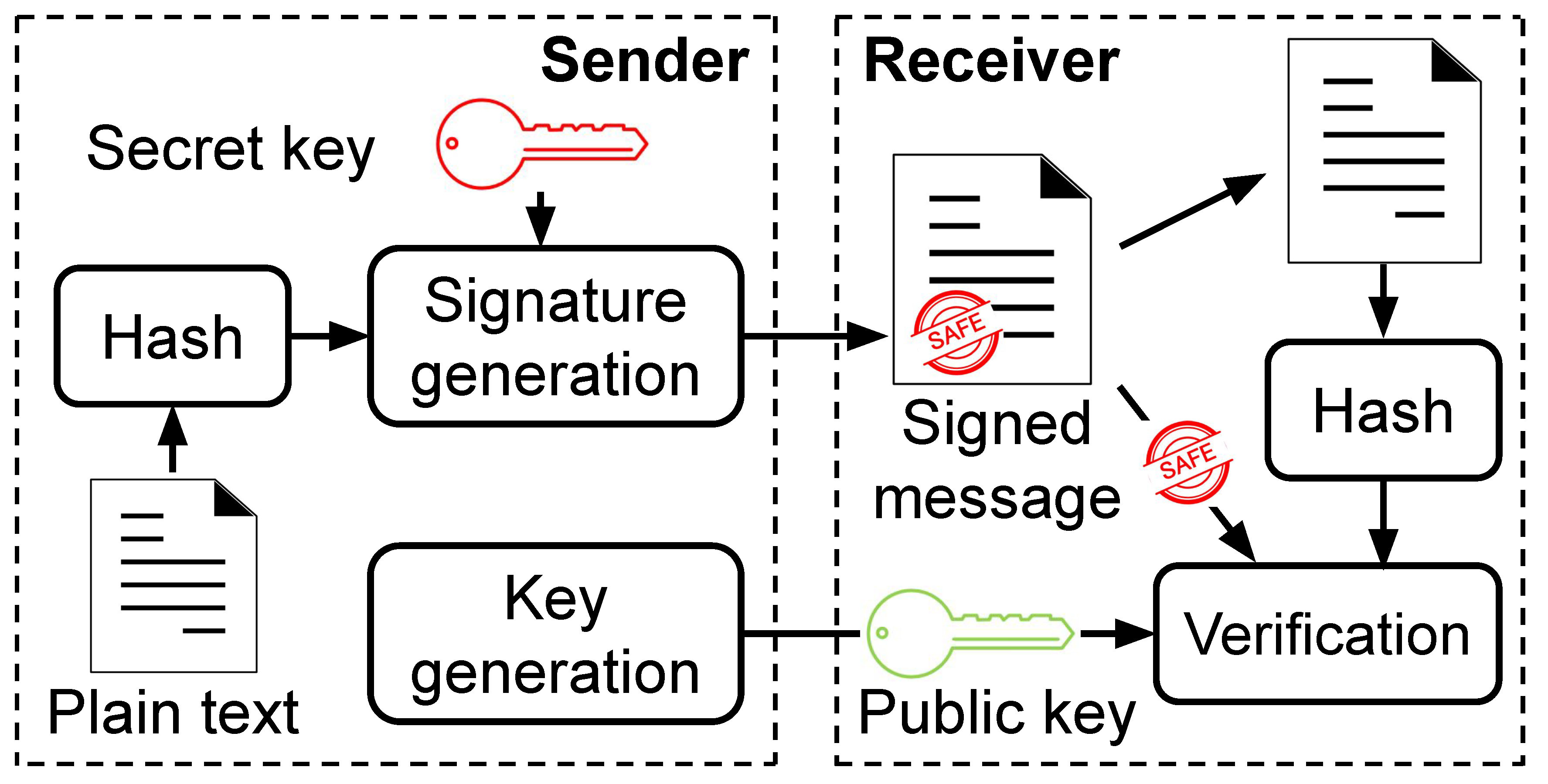
2.1. Digital Signature Algorithm

Digital signatures are effective in providing the authentication, integrity, and non-repudiation of messages. The digital signature algorithm (DSA) was adopted as a digital signature standard (DSS) by NIST from 1994. The DSA algorithms include three main stages. The first one is the key-generation stage, where the sender generates a public key from a random number. The generated key is then sent with the message and used to verify the signature. The second one is the signature-generation stage, where the sender generates the signature for the message based on a secret key and the hash of the message. The message is then digitally signed with this signature. The last one is the verification stage. In this stage, the receiver verifies the validity of the message by using the public key and the signature. The message is considered valid if the recovered signature matches the received signature. Figure 1 illustrates the three stages of DSA.

2.2. Elliptic Curve Digital Signature Algorithm—ECDSA

The high level of security of ECC relies on the difficulty level of the elliptic curve discrete logarithm problem (ECDLP). ECDSA depends on the elliptic curve cryptosystem. Like the other DSA, ECDSA has three stages. In the key-generation stage, a random number is multiplied by the base point of the selected curve to compute the public key. In the signature-generation stage, based on a secret key, a point multiplication and a hash function, additions are performed to find the signature. In the verification stage, the receiver recovers the signature from the received message and the public key, then compares it with the received signature. If the two signatures are identical, the received message is valid. Algorithm 1 explains ECDSA in detail.
Algorithm 1 Elliptic curve digital signature algorithm (ECDSA).
Key-generation
Input: Prime p, base point G
Output: Public key Q
  1: Select a random number d where 1 d n 1
  2: Compute Q = d G over the prime field F p
 
Signature generation
Input: Prime p, base point G, and the private key d
Output: Signature ( r , s ) for the message m
  1: Select a random number k where 1 k p 1
  2: Compute ( x 1 , y 1 ) = k G over the prime field F p
  3: Assign r = x 1
  4: Compute e = H a s h ( m )
  5: Compute s = k 1 ( e + d r ) over the prime field F p
 
Verification
Input: Prime p, base point G, signature ( r , s ) of the input message m, public key Q
Output: The input message m is valid or invalid
  1: Compute e = H a s h ( m )
  2: Compute w = s 1 over the prime field F p
  3: Compute v 1 = e w over the prime field F p
  4: Compute v 2 = r w over the prime field F p
  5: Compute ( x 1 , y 1 ) = v 1 G + v 2 Q over the prime field F p
  6: if ( x 1 , y 1 ) = O where O is the point at infinity then
  7:     State message m is invalid
  8: else
  9:     Assign v = x 1
  10: end if
  11: if v = r then
  12:     State message m is valid
  13: else
  14:     State message m is invalid
  15: end if

2.3. Edwards-Curve Digital Signature Algorithm—EdDSA

The EdDSA is based on the Edwards curves developed by Bernstein et al. The security of Ed25519 and Curve25519 are based on ECDLP. Ed25519 has three stages. In the key-generation stage, a public key is generated from a secret key and the based point of Curve25519. In the signature-generation stage, a pair of signatures is produced from the private key and the hash of the input message. The signature is then attached with the message and sent to the receiver. Finally, the received signature and the public key by the receiver are used to verify the message in the verification stage. Algorithm 2 reviews EdDSA in detail.
Algorithm 2 Edwards-curve digital signature algorithm (EdDSA).
Key-generation
Input: Prime p, base point G, private key k
Output: Public key Q
  1: Compute ( h k , l k ) = H a s h ( k ) where h k is 32 bytes MSB and l k is 32 bytes LSB.
  2: Assign a = h k as little-endian notation
  3: Compute Q = a G over the prime field F p
 
Signature-generation
Input: Prime p and q, base point G, private key k, public key Q, and message m
Output: Signature ( R , s ) for the message m
  1: Compute ( h k , l k ) = H a s h ( k ) where h k is 32 bytes MSB and l k is 32 bytes LSB.
  2: Compute r = H a s h ( l k , m ) mod q
  3: Compute R = r G over the prime field F p
  4: Compute h = H a s h ( R , Q , m ) mod q
  5: Compute s = ( r + h a ) mod q
 
Verification
Input: Prime p and q, base point G, signature ( R , s ) of the input message m, public key Q
Output: The input message m is valid or invalid
  1: Compute h = H a s h ( R , Q , m ) mod q
  2: Compute h Q = R + h Q over the prime field F p
  3: Compute s G = s G over the prime field F p
  4: if h Q = s G then
  5:    State message m is valid
  6: else
  7:    State message m is invalid
  8: end if

2.4. ECDSA/EdDSA Hierarchy

The hierarchy of the ECDSA/EdDSA combinational design can be illustrated as Figure 2. In this illustration, the operations in the higher position are performed based on the operations in the lower position. Figure 2 also reveals that there are three different layers of abstraction. The first layer is the DSA algorithm, where the processes of key-generation, signature-generation, and verification of a specific DSA are specified. The control flow for a DSA, such as ECDSA or EdDSA, is implemented in this layer. The second layer is the algorithms for the elliptic curve. Depending on the selected curve, the additions and subtractions between two points in this curve are defined. The point multiplication can be used for different curves. The third layer describes the methods of modular operations, such as modular multiplication, inversion, addition, and subtraction. An additional modular reduction may be required for this layer. Finally, the base of all layers is binary addition, subtraction, and comparison. Among these layers, the implementation for point multiplication, modular multiplication, modular inversion, modular addition, modular subtraction, and binary operation can be reused. In Figure 2, the gray boxes illustrate the functions that could be shared among different elliptic curves.

3. Hardware Architecture

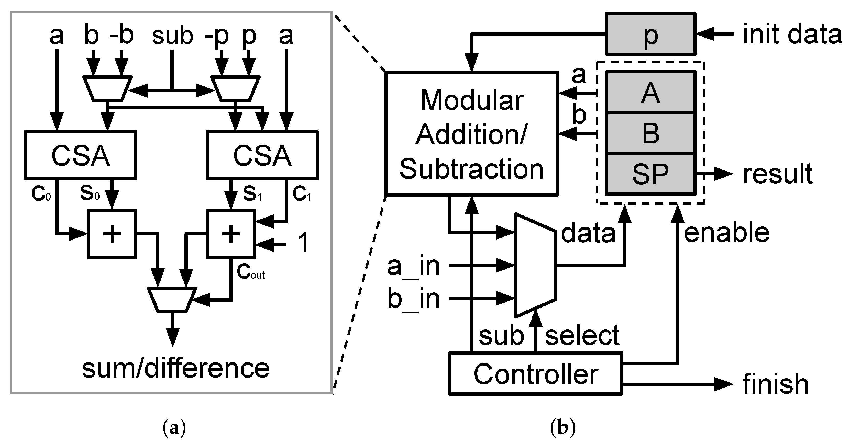
3.1. Modular Arithmetic-Logic Unit

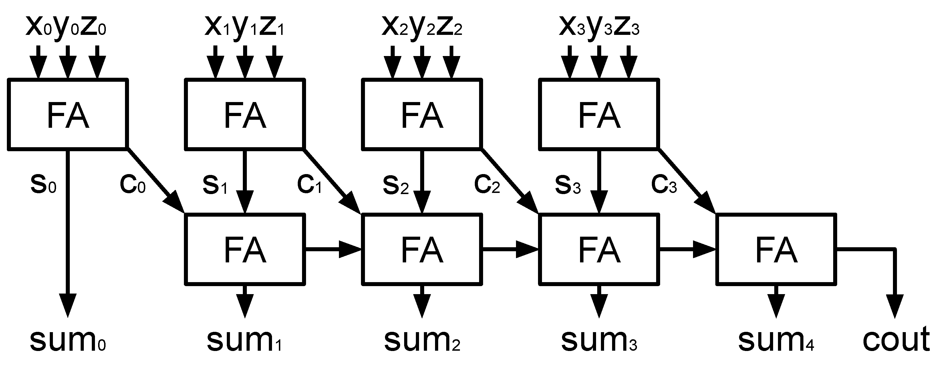
3.1.1. Modular Addition/Subtraction

The base of ECC algorithms is modular operations. Figure 3 shows the combinational architecture of modular addition/subtraction. This module could perform both addition and subtraction with the modularity of a prime number p. The architecture is split into two branches. The left branch performs the operation without p, and the right branch performs the operation with p. When the s u b signal is activated, the multiplexer at the left-side selects b , then < a b > is performed, while the multiplexer at the right-side selects p and then the addition circuit performs < a b + p > . When the s u b signal is inactivated, < a + b > is calculated on the left circuit, and < a + b p > is calculated on the right circuit. The final value is selected depending on the carry out of the right branch. In this architecture, the carry save adders (CSAs) are used to reduce the logic delay of the three-operands additions.
Figure 4 illustrates the architecture CSAs that are used in Figure 3. A three-operands CSA includes two layers. In the first layer, the corresponding bits from each operand are simultaneously added together using full adders (FAs). The results of the first layer is the sum bits [ s 0 ... s n ] and the carry bits [ c 0 ... c n ]. In the second layer, a ripple–carry addition is performed between the generated sum and carry from the first layer. The result of this layer is the final result of the three-operands addition. The delay of CSA is the total delay of two layers. The delay of the first layer is equal to the delay of a 1-bit FA. The delay of the second layer is the delay of the two-operands adder. Figure 5 illustrates the architecture of a conventional three-operands adder. Two operands are added in the first layer, and then the result is added with the third operands in the second layer. Figure 4 and Figure 5 reveal that the conventional three-operand adder suffers more ripple carry delay from two consecutive adders while using the same resource as CSA.

3.1.2. Processing Element

The processing element (PE) includes an addition/subtraction module and a controller. The controller drives the addition/subtraction module to perform modular additions, subtractions, or multiplications. In our design, the addition/subtraction module naturally performs the modular reduction in each operation; there is no need for an additional modular reduction module. Each PE contains three registers. In the case of addition and subtraction, two registers are used to store the operands (registers A and B), and the sum/product (SP) register stores the sum or difference. In the case of multiplication, the multiplier and multiplicand are stored in registers A and B; the product is put into register SP. During the multiplication, the multiplier is shifted for each cycle. Depending on the width of the operands, the multiplication could be performed in multiple cycles. The final result is valid when the finish signal is activated. Figure 3 illustrates the architecture of the processing element. The register p is used to store the prime number for the modular operations. It is shared among different PEs in the system.

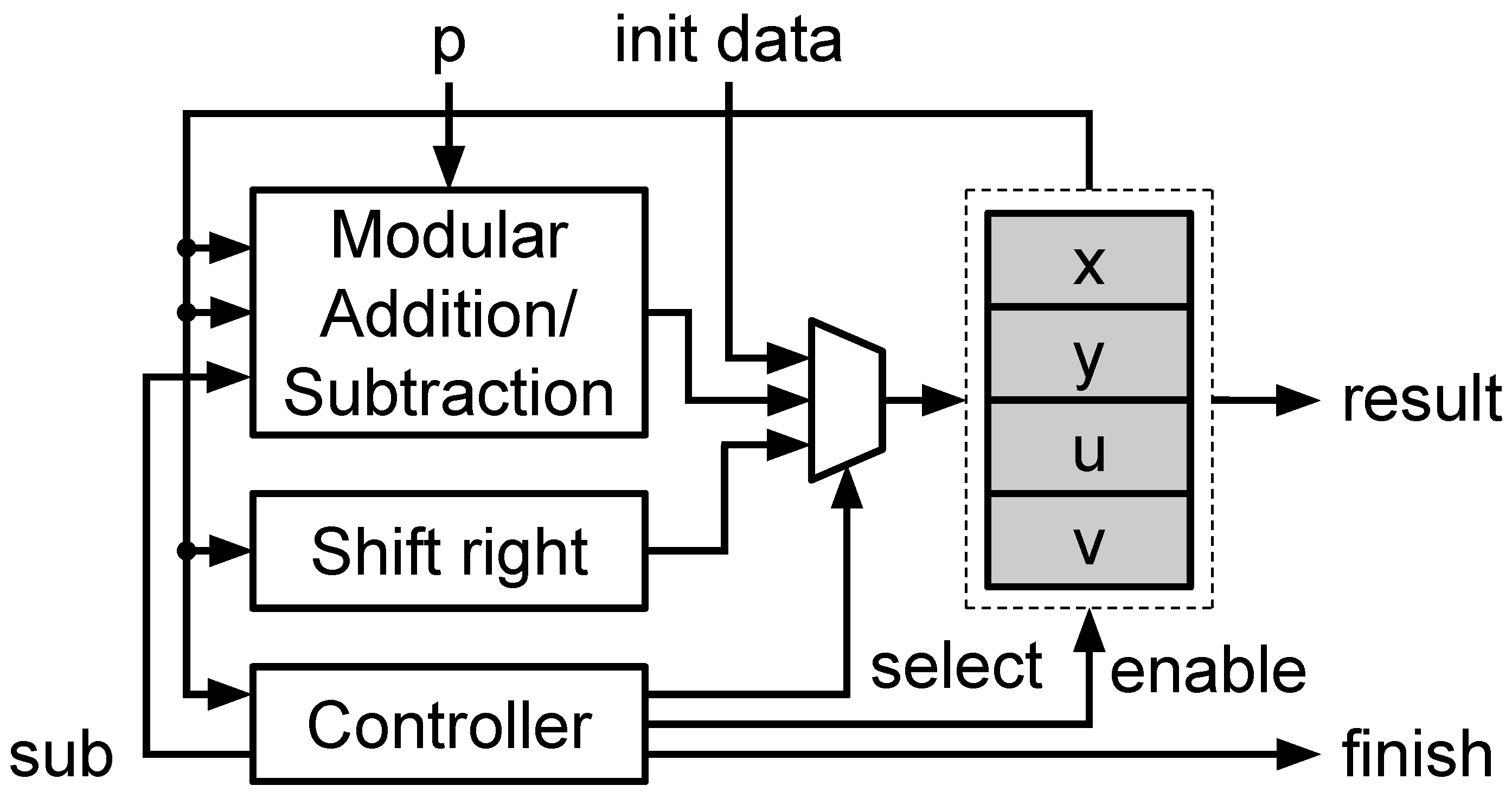
3.1.3. Modular Inversion

In our design, the modular inversion is calculated by using the binary Euclidean algorithm (BEA) [20]. BEA is the traditional method that can calculate the inversion of a number over the prime field. It is independent of the usage of the ECC algorithm. Therefore, it is the most suitable for a multi-functional design. Algorithm 3 reveals the binary Euclidean algorithm. Figure 6 shows the optimized hardware implementation of BEA in our proposed architecture. The BEA memory system includes four registers to store the temporal data during calculation. The datapath contains a modular addition/subtraction and a right shift circuit. The controller determines the updated register and the source of updated data. The controller of the modular inversion module is based on a finite state machine (FSM). Depending on Algorithm 3, the FSM includes the following states: calculate new value of u; calculate new value of v; compare new value of u and v; update the value of u; update new value of v; calculate new value of x; calculate new value of y; update x; update y; check the condition; and assign the final result. BEA contains three kinds of operation, which are right shift, modular addition, and modular subtraction. Based on our design of FSM, only one modular addition/subtraction module and one shift right module are needed. Finally, after the calculation process is completed, the final result is assigned for y, and the system raises the finish signal to indicate that the process is finished.
Algorithm 3 Binary Euclidean algorithm (BEA).
Input: Prime p and a [ 1 , p 1 ]
Output: a 1 mod p
  1: u a , v p , x 1 , y 0
  2: while u 1 and v 1 do
  3:    while u mod 2 = 0  do
  4:          u u 1
  5:         if x mod 2 = 0  then
  6:             x x 1
  7:         else
  8:             x ( x + p ) 1
  9:         end if
  10:    end while
  11:    while v mod 2 = 0 do
  12:         v v 1
  13:        if y mod 2 = 0  then
  14:             y y 1
  15:        else
  16:             y ( y + p ) 1
  17:        end if
  18:    end while
  19:    if  u v  then
  20:         u ( u v ) mod p
  21:         x ( x y ) mod p
  22:    else
  23:         v ( v u ) mod p
  24:         y ( y x ) mod p
  25:    end if
  26: end while
  27: if u = 1 then
  28:      return x
  29: else
  30:      return y
  31: end if

3.2. Elliptic Curve Cryptography Unit

The ECC unit is the top module of the system. It includes a controller, a random access memory (RAM), a read-only memory (ROM), an inversion module (Inv.), and four PEs. Figure 7 illustrates the architecture of the ECC unit. In our design, the point adding and doubling for both ECDSA and EdDSA are performed under projective coordination. The conversion from affine to projective coordination is performed without any additional fee. In comparison with other types of coordination, projective coordination offers optimization for parallelism processing by reducing data dependency. Four PEs and an inversion module are integrated to achieve the highest performance in projective coordination.
Each processing element and inversion module has their register to store the temporal data during their operation. The input data for each PE are selected from the RAM, the initial data from ROM, the calculated data from the other PEs, and the generated data by themselves. The controller controls the operations of the four PEs and the inversion module to produce the appropriate results. The FSM of the ECC unit controller is designed to promote the parallelism of the four PEs. The RAM is used for multiple purposes: to store the data/result and exchange data among the PEs. The result is read from RAM in a specific address. When the operation of the processing elements and the inversion module is completed, the controller raises the finish signal to indicate that the result is valid and it can be read.

4. Results

We deploy our design on the field-programmable gate array (FPGA) Virtex-7 and Virtex-6 devices. Two different designs are used in the experiments. We use Xilinx ISE 14.7 to implement our design on Virtex-6 device, and Vivado 2020.1 for Virtex-7 device. The first one is integrated with Ed25519 and ECDSA with NIST P-256. The second one is the combination of Ed25519 and ECDSA with NIST P-256, P-384, and P-521. The results and comparison are shown in Table 1. The input message and parameters are taken from [2] for the ECDSA mode and from [6] for the Ed25519 mode.
It is clear that our design consumes significantly lower resources in comparison with other proposals. The four-mode design also uses fewer resources than the ECDSA P-256, ECDSA P-384, and ECDSA P-521 single-functional core of [11]. In addition, our design supports all functions of DSA, including sign, verify, and key generation (Keygen). The authors of [21] proposed a multi-core architecture that can generate up to 21,686 keys per second. Despite the throughput and the number of Slices 2 /Ops being impressive, their design requires too many resources for only key generation, and its practical applications are limited. In this experiment, we estimate a DSP as 100 slices [9] to calculate the slices equivalently. The comparison is performed based on the number of slices, number of DSPs, and the working frequency (Freq) in MHz. Other technical details, including Slices 2 /MHz, Slices 2 /Ops, throughput in kilo-bits-per-second (Kbps), and Slices 2 /Kbps, are added to evaluate the efficiency of the design. In this study, we target a low-resource, multi-functional design. Therefore, the number of slices is emphasized rather than the other aspects.
The ECPM is the essential part of an elliptic curve cryptography design. We also compare our processing core, with four PEs, with other proposals in Table 2. Table 2 reveals that the processing core occupies nearly 70% of the total resource. In comparison with other ECPM proposals, the resource consumption of our ECPM design is significantly lower, even though the core supports multiple curves. Table 2 also reveals that the DSP-based architectures [13,22] provides high throughput but consumes too many resources for a single curve. Therefore, they cannot be deployed on resource-constrained applications.
We also deploy our system on the Xilinx VC707 Evaluation Kit. Figure 8 illustrates the experimental system, including a RISC-V softcore processor, a Secure Hash Algorithm 2 (SHA2) core, and the EdDSA/ECDSA core with Curve25519 and NIST P-256/384/521. The RISC-V processor communicates with the SHA2 core and EdDSA/ECDSA core through a communication bus. The implemented SHA2 core could perform three SHA2 variants, which are SHA2-256, SHA2-384, and SHA2-512 in a single design. The RISC-V processor configures the operating mode for the SHA2 core and EdDSA/ECDSA core, controls the SHA2 core to perform the hash on the input message, and then transfers the hash value to the EdDSA/ECDSA core. When the EdDSA/ECDSA process terminates, the processor reads the results and then compares them with the correct results in [2,6]. A computer connects with the RISC-V processor through UART to monitor the experimental process. Such a design system allows the processor to perform the SHA2 hash process and EdDSA/ECDSA process at the same time. Furthermore, the SHA2 functions and EdDSA/ECDSA functions can be used separately.

5. Conclusions

In this study, a low-cost, area-efficient ECC processor is developed for multiple ECC algorithms in a single design. Based on the proposed architecture, four well-known algorithms, which are Ed25519, ECDSA with NIST P-256, NIST P-384, and NIST P-521, are deployed. The novel hardware architecture satisfies multiple requirements that were trade-offs from the previous designs. It consumes significantly few resources and does not use any DSP. Therefore, it can be easily deployed on multiple hardware platforms without re-design. Especially, this proposal provides an approach to deploy multiple ECC algorithms in a single architecture without re-synthesis.
In the experiments, we suggest a system that can improve the flexibility of the design. By combining with a separate SHA2 processor, the system not only performs the EdDSA/ECDSA, but also the SHA2 hash functions. The experimental results show that the core consumes 10,259 slices, which is lower than other single-functional ECC designs and can run up to 112.2 MHz on a Virtex-7 device. Another implementation that can perform two lightweight ECC algorithms, which are Ed25519 and ECDSA with NIST-P256, is also deployed. It consumes only 4276 slices and can run up to 122.05 MHz on the Virtex-7 device. Based on the features of the proposed EdDSA/ECDSA core and the experimental results, it can be concluded that our design can serve a wide range of applications and be able to deploy on multiple hardware platforms, especially for the resource-constrained devices that need a high level of security.
For future works, we are working on higher performance for the processing elements. Two targets can be achieved if the processing elements are able to operate with a lower delay but keep the same resource usage. For the first target, our core can provide higher overall performance while ensuring efficiency in the area. For the second target, the resource consumption can be further reduced by removing some processing elements while maintaining the current working performance.

Author Contributions

Supervision, C.-K.P. and T.-T.H.; methodology, B.K.-D.-N. and T.-T.H.; investigation, B.K.-D.-N., C.P.-Q. and N.-T.T.; writing—original draft preparation, B.K.-D.-N.; writing—review and editing, C.-K.P. and T.-T.H. All authors have read and agreed to the published version of the manuscript.

Funding

This research was funded by New Energy and Industrial Technology Development Organization (NEDO) project JPNP16007.

Institutional Review Board Statement

Not applicable.

Informed Consent Statement

Not applicable.

Data Availability Statement

No new data were created or analyzed in this study. Data sharing is not applicable to this article.

Acknowledgments

This paper is based on results obtained from project JPNP16007, commissioned by the New Energy and Industrial Technology Development Organization (NEDO).

Conflicts of Interest

The authors declare no conflict of interest.

References

  1. The Transport Layer Security (TLS) Protocol Version 1.3. Available online: https://www.rfc-editor.org/info/rfc8446 (accessed on 10 March 2022).
  2. IKE and IKEv2 Authentication Using the Elliptic Curve Digital Signature Algorithm (ECDSA). Available online: https://www.rfc-editor.org/info/rfc4754 (accessed on 10 March 2022).
  3. IT Security Techniques—Digital Signatures. Available online: https://www.iso.org/standard/76382.html (accessed on 10 March 2022).
  4. Digital Signature Standard (DSS). Available online: https://csrc.nist.gov/publications/detail/fips/186/2/archive/2000-01-27 (accessed on 10 March 2022).
  5. Public Key Cryptography for the Financial Services Industry: The Elliptic Curve Digital Signature Algorithm (ECDSA). Available online: https://standards.globalspec.com/std/1955141/ANSI%20X9.62 (accessed on 10 March 2022).
  6. Edwards-Curve Digital Signature Algorithm (EdDSA). Available online: https://www.rfc-editor.org/info/rfc8032 (accessed on 10 March 2022).
  7. Bernstein, D.; Duif, N.; Lange, T.; Schwabe, P.; Yang, B.Y. High-Speed High-Security Signatures. J. Cryp. Eng. 2011, 2, 124–142. [Google Scholar]
  8. Sghaier, A.; Zeghid, M.; Machhout, M. Fast hardware implementation of ECDSA signature scheme. In Proceedings of the International Symposium on Signa, Image, Video and Communications (ISIVC), Tunis, Tunisia, 21–23 November 2016; IEEE: Piscataway, NJ, USA, 2017; pp. 343–348. [Google Scholar]
  9. Sghaier, A.; Zeghid, M.; Massoud, C.; Mahchout, M. Design And Implementation of Low Area/Power Elliptic Curve Digital Signature Hardware Core. Electronics 2017, 6, 46. [Google Scholar] [CrossRef] [Green Version]
  10. Panjwani, B.; Mehta, D.C. Hardware-software co-design of elliptic curve digital signature algorithm over binary fields. In Proceedings of the International Conference on Advances in Computing, Comm. and Informatics (ICACCI), Kochi, India, 10–13 August 2015; IEEE: Piscataway, NJ, USA, 2015; pp. 1101–1106. [Google Scholar]
  11. Panjwani, B. Scalable and parameterized hardware implementation of elliptic curve digital signature algorithm over prime fields. In Proceedings of the International Conference on Advances in Computing, Comm. and Informatics (ICACCI), Udupi, India, 13–16 September 2017; IEEE: Piscataway, NJ, USA, 2017; pp. 211–218. [Google Scholar]
  12. Bisheh-Niasar, M.; Azarderakhsh, R.; Mozaffari-Kermani, M. Cryptographic Accelerators for Digital Signature Based on Ed25519. IEEE Trans. Very Large Scale Integr. (VLSI) Syst. 2021, 29, 1297–1305. [Google Scholar] [CrossRef]
  13. Salarifard, R.; Bayat-Sarmadi, S. An Efficient Low-Latency Point-Multiplication Over Curve25519. IEEE Trans. Circ. Syst. I Regul. Pap. 2019, 66, 3854–3862. [Google Scholar] [CrossRef]
  14. Sasdrich, P.; Güneysu, T. Implementing Curve25519 for Side-Channel–Protected Elliptic Curve Cryptography. ACM Trans. Embed. Comput. Syst. 2015, 9, 1–15. [Google Scholar] [CrossRef]
  15. Turan, F.; Verbauwhede, I. Compact and Flexible FPGA Implementation of Ed25519 and X25519. ACM Trans. Embed. Comput. Syst. 2019, 18, 1–21. [Google Scholar] [CrossRef]
  16. Asif, S.; Hossain, M.S.; Kong, Y. High-throughput multi-key elliptic curve cryptosystem based on residue number system. IET Comp. Dig. Tech. 2017, 5, 165–172. [Google Scholar] [CrossRef]
  17. Islam, M.M.; Hossain, M.S.; Hasan, M.K.; Shahjalal, M.; Jang, Y.M. FPGA Implementation of High-Speed Area-Efficient Processor for Elliptic Curve Point Multiplication Over Prime Field. IEEE Access 2019, 7, 178811–178826. [Google Scholar] [CrossRef]
  18. Kodali, R.K. Implementation of ECDSA in WSN. In Proceedings of the International Conference on Control Communication and Computing (ICCC), Thiruvananthapuram, India, 13–15 December 2013; IEEE: Piscataway, NJ, USA, 2014; pp. 310–314. [Google Scholar]
  19. Cheng, H.; Liu, J.; Mao, J.; Wang, M.; Chen, J.; Bian, J. A Compatible OpenFlow Platform for Enabling Security Enhancement SDN. Sec. Commun. Netw. 2018, 2018, 8392080. [Google Scholar] [CrossRef] [Green Version]
  20. Sunar, B. Binary Euclidean Algorithm. In Encyclopedia of Cryptography and Security; van Tilborg, H.C.A., Ed.; Springer: Boston, MA, USA, 2005; pp. 31–32. [Google Scholar] [CrossRef]
  21. Sasdrich, P.; Güneysu, T. Efficient Elliptic-Curve Cryptography Using Curve25519 on Reconfigurable Devices. In Proceedings of the Applied Reconfigurable Computing (ARC), Vilamoura, Portugal, 14–16 April 2014; Goehringer, D., Santambrogio, M.D., Cardoso, J.M.P., Bertels, K., Eds.; Springer: Cham, Switzerland, 2014; pp. 25–36. [Google Scholar]
  22. Koppermann, P.; De Santis, F.; Heyszl, J.; Sigl, G. X25519 Hardware Implementation for Low-Latency Applications. In Proceedings of the Digital Syst. Design (DSD), Limassol, Cyprus, 31 August–2 September 2016; IEEE: Piscataway, NJ, USA, 2016; pp. 99–106. [Google Scholar]
Figure 1. Digital signature algorithm.
Cryptography 06 00025 g001
Figure 2. ECDSA/EdDSA hierarchy.
Cryptography 06 00025 g002
Figure 3. (a) Modular addition/subtraction architecture. (b) Processing element architecture.
Cryptography 06 00025 g003
Figure 4. Three-operands carry save adder.
Cryptography 06 00025 g004
Figure 5. Three-operands conventional adder.
Cryptography 06 00025 g005
Figure 6. Modular inversion architecture.
Cryptography 06 00025 g006
Figure 7. Elliptic curve cryptography unit.
Cryptography 06 00025 g007
Figure 8. Experimental system.
Cryptography 06 00025 g008
Table 1. ECDSA/EdDSA comparison, ●/○ represents for supported/not-supported.
This Work[11][15][21]
Support
Mode
EdDSA25,519
ECDSAP-256
P-384
P-521
Support
Func.
Sign
Verify
Keygen
FPGAVirtex-6Virtex-7Virtex-6Virtex-7Virtex-6Virtex-6Virtex-6Artix-7Artix-7
Slices43274276861010,25910,62516,74723,633430311,277
DSP000013619628016220
Slices equivalent43274276861010,25924,22536,34751,633590333,277
Frequency (MHz)116.72122.0572112.210083.371.582100
Slices 2 /MHz × 10 3 1601501030938586915,86037,28642511,074
Operations
per
sec.
(Ops)
Ed25519Sign12713278122---118-
Verify55573453---78-
Keygen12513177120---9021,686
ECDSA
P-256
Sign10811367104787----
Verify55573453674----
Keygen10911367104-----
ECDSA
P-384
Sign--3047-292---
Verify--1523-276---
Keygen--3047-----
ECDSA
P-521
Sign--1625--109--
Verify--813--83--
Keygen--1626-----
Slices 2 /Ops × 10 3 Ed25519Sign148138950865---295-
Verify34131821881994---447-
Keygen150140960875---38751
ECDSA
P-256
Sign17316111091011746----
Verify34232021982003871----
Keygen17316111071009-----
ECDSA
P-384
Sign--24742254-4524---
Verify--49364497-4790---
Keygen--24712251-----
ECDSA
P-521
Sign--45324129--24,458--
Verify--90678260--32,120--
Keygen--45284125-----
Table 2. Elliptic curve point multiplication comparison, ●/○ represents for supported/not-supported.
This Work[17][16][13][22]
Support
Curve
25519
P-256
P-384
P-521
FPGAVirtex-6Virtex-7Virtex-6Virtex-7Virtex-6Virtex-7Virtex-7Kintex-7Kintex-7
Slices30252932595771729246887324,20033628639
DSP0000000182260
Slices equivalent30252932595771729246887324,20021,56234,639
Frequency (MHz)116.72149.2388.82138.58161.1177.772.987115
Slices 2 /MHz × 10 3 78584003715314438033534410,434
Through-
put
(Kbps)
255199111769108---57732159
P-256114146871351571731816--
P-384--5890-----
P-521--4366-----
Slices 2 /Kbps
× 10 3
2551910074511475---81556
P-2568059409380545455322--
P-384--614570-----
P-521--833774-----
Publisher’s Note: MDPI stays neutral with regard to jurisdictional claims in published maps and institutional affiliations.

