Article

HAIPO: Hybrid AI Algorithm-Based Post-Fabrication Optimization for Modern 3D NAND Flash Memory

School of Computer Science and Engineering, Kyungpook National University, Daegu 37224, Republic of Korea
Processes 2024, 12(12), 2760; https://doi.org/10.3390/pr12122760
Submission received: 22 November 2024 / Accepted: 2 December 2024 / Published: 4 December 2024
(This article belongs to the Section Manufacturing Processes and Systems)

Abstract

:
To successfully meet the various requirements of modern storage systems, NAND flash memory should be highly optimized by precisely tuning a huge number of internal operating parameters. Although 3D NAND flash memory succeeds in increasing the capacity of storage systems, its complex architecture and unique error behavior make such optimization a more difficult and time-consuming process during NAND manufacturing. In this paper, we introduce HAIPO, a novel methodology for post-fabrication optimization of NAND flash memory, which is an essential step in the manufacturing process of modern 3D NAND flash memory to simultaneously meet various requirements on reliability, performance, yield, etc. HAIPO is based on simple machine-learning approaches that consist of (i) a lightweight deep-learning (DL) model to generate initial device parameters and (ii) an evolutionary algorithm (EA) to explore device parameters automatically. To more effectively explore device parameters, we introduce three key guidelines for each generation in the EA: (1) domain-specific rules, (2) recent optimization results, and (3) online Bayesian simulation, respectively, to enable quick optimization for a huge number of device parameters within the limited product turnaround time (TAT). In addition, we integrate two optimization modules with HAIPO to improve optimization efficiency even in environments with severe process variation. We demonstrate the feasibility and effectiveness of HAIPO using real 320 3D TLC/QLC NAND flash chips, showing significant performance and reliability improvements by up to 8.8% and 12% on average, respectively, within a quite limited optimization TAT.

1. Introduction

NAND flash memory is the key memory technology in architecting modern storage systems. NAND flash-based solid-state drives (SSDs) provide various advantages over traditional hard disk drives (HDDs), such as high performance, low power consumption, and small form factor while achieving high device capacity (e.g., several tens of terabytes per SSD [1,2,3,4]). However, due to the rapid expansion of the data-centric computing market, NAND flash-based solid-state drives (SSDs) are faced with new challenges that should meet various requirements simultaneously. For example, data center applications require quality of service (QoS), in which 99.99% or 99.9999% of the total read requests should be performed without delay in response time. In addition, due to the explosive increase in data generation, NAND flash memory is required to satisfy large capacity, high reliability, and high performance at the same time.
To successfully implement a mass production system based on high yield while satisfying various requirements of modern applications, post-fabrication optimization. (Generally, many NAND manufacturers and storage companies have referred to tuning eFuses to improve their characteristics after manufacturing the chip as “post-manufacturing optimization”. In our paper, we use the term “optimization” following such a convention.) is an essential step in the manufacturing process of modern NAND flash memory. After fabricating a chip, manufacturers configure various device parameters (e.g., the voltage/timing parameters for read/program/erase operations) that determine the chip’s performance, reliability, and yield. Chip information related to device parameters is stored in special NAND flash cells. (The minimum unit for storing data in NAND flash memory is called a flash cell.) During system booting, the NAND flash chip reads the chip information stored in the special NAND flash cells according to the power-up sequence. The NAND flash chip moves it into a register-type circuit with a latch structure called an eFuse (electrical fuse) in peripheral circuits to access the chip information. All device parameters affecting the NAND flash memory characteristics (i.e., reliability and performance) are determined by the combinations of eFuse values. Post-fabrication optimization is a complex and time-consuming process that determines the best device parameters based on the optimized eFuse combinations.
Traditionally, post-fabrication optimization has been manually done by experienced engineers at NAND manufacturers. However, manual-based post-fabrication optimization is no longer practical in modern high-capacity 3D NAND flash chips for three reasons. First, the number of device parameters to optimize for a single chip has significantly increased. For example, a modern triple-level cell (TLC) NAND flash chip has more than thousands of device parameters that must be carefully configured depending on the physical characteristics of target NAND flash cells. Second, there exists a complex trade-off correlation between NAND flash memory performance, reliability, and yield. For example, improving performance can lead to reliability degradation or make it difficult to secure high yields. Moreover, in modern NAND flash chips, such correlation between device characteristics shows significant variations between flash chips, flash blocks within a single chip, and even pages in a single block. (Generally, a NAND flash chip consists of thousands of blocks, and a single block comprises multiple pages.) Therefore, the difficulty of post-fabrication optimization increases exponentially as NAND flash memory technologies are advanced. Finally, post-fabrication optimization is a time-critical task. To meet the limited product turnaround time (TAT), i.e., the amount of time taken to complete the chip production since the start of development, post-fabrication optimization should be completed in quite a short time (e.g., a few days). Therefore, manually optimizing a large number of device parameters within a limited time requires significant human effort and often fails to obtain optimal results.
To address the challenges in post-fabrication optimization, we introduce HAIPO (Hybrid AI Algorithm-based Post-fabrication Optimization), a new post-fabrication optimization scheme that enables optimizing modern high-density 3D NAND flash memory to better meet various performance, reliability, and yield requirements within the limited optimization TAT during NAND manufacturing. HAIPO aims to automatically search and find the optimal eFuse combinations based on deep learning (DL) [5] and evolutionary algorithm (EA) [6]. HAIPO uses (i) a lightweight deep-learning (DL) model to generate initial device parameters that can roughly meet the given design requirements and (ii) an evolutionary algorithm (EA) to automatically explore device parameters from the initial values. In addition, to more carefully yet more extensively explore the device parameter sets (i.e., populations), HAIPO introduces three key guidelines for each generation in the EA to generate device parameters. First, it ensures that each population satisfies a set of predefined rules based on domain-specific knowledge from experienced engineers. If the EA generates a value that violates any rules, HAIPO chooses a random value that meets all related rules. Second, HAIPO checks that every device parameter is in a desirable value range based on the recent populations (i.e., newborns) that provide the highest performance and reliability levels (i.e., the highest achievement score). Third, HAIPO simulates the optimization level of each population based on a simple Bayesian model (trained online with real-measurement results) to select the best populations to be tested on real chips. By doing so, we can effectively evaluate a large number (e.g., ∼ 10 7 ) of populations within the limited measurement times, which accelerates the entire post-optimization process. In addition, to further improve the efficiency and robustness of our HAIPO, we integrate two optimization modules with our technique. These modules enable HAIPO both to take into account chip variation due to complex 3D manufacturing processes and to improve the optimization TAT in an environment where multiple requirements must be satisfied simultaneously.
To validate the effectiveness of our technique, we evaluate HAIPO using 320 real state-of-the-art 3D TLC/QLC NAND flash chips. Our results show that HAIPO improves the performance and reliability of NAND flash chips by 12% and 8.8% on average, respectively. Furthermore, HAIPO efficiently reduces the total optimization TAT up to 70% compared with the manual-based optimization.
The rest of this paper is organized as follows. In Section 2, we review the overview of NAND flash memory and NAND eFuse tuning operations. Section 3 provides a key concept of NAND post-fabrication optimization. In Section 4, we present a design and implementation of our technique, HAIPO. The experimental results follow in Section 5, and the related work is summarized in Section 6. Section 7 concludes with a summary and future work.

2. Background

We provide a brief background on modern NAND flash memory, which is necessary to understand the rest of the paper.

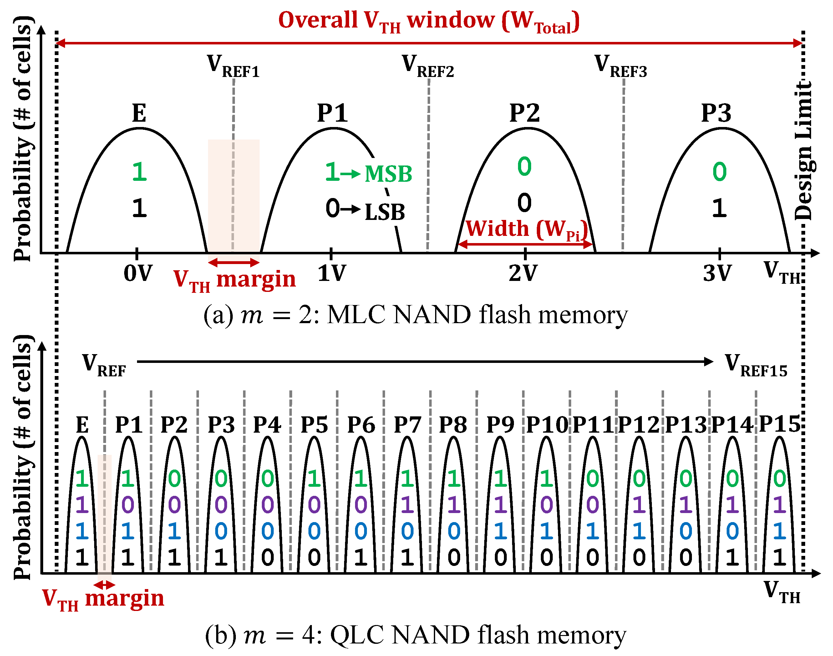
2.1. Overview of NAND Flash Memory

NAND Flash Organization. The NAND flash memory consists of flash cells, which store data, and peripheral circuits, which support flash commands such as read and write. Flash cells are grouped into a page, and multiple pages form a block. Figure 1 illustrates the hierarchical organization of a NAND flash chip. A set of flash cells form a NAND string that is connected to a bitline (BL), and NAND strings of different BLs compose a block. The control gate of each flash cell at the same vertical location in a block is connected to a wordline (WL), so all the cells at the same WL (i.e., sharing WL) concurrently operate. Thousands of blocks constitute a plane while sharing all the BLs in the plane. There are typically two or four planes in a single NAND flash chip (or die).
Data Storage Mechanism. A flash cell stores bit data as a function of its threshold voltage ( V t h ) level that highly depends on the amount of charge in the cell’s charge trap layer; the more electrons in the charge trap layer, the higher the cell’s V t h level. Depending on the number of electrons in the cell’s charge trap layer, the flash cell works as an off switch or an on switch under a given control gate voltage (i.e., WL gate voltage), thus effectively storing bit data. For example, we can assign a ‘0’ state when the flash cell has a high V t h and a ‘1’ state when the flash cell has a low V t h . Since the flash cell is surrounded by dielectric materials, electrons in the charge trap layer are electrically insulated. This cell organization gives NAND flash memory a non-volatile characteristic so that the electrons trapped in the flash cell do not leak even after the power is off.
NAND Flash Operations. There are three basic operations to access or modify the data stored in NAND flash memory: (i) program, (ii) read, and (iii) erase operations. The program operation, which increases V t h of selected flash cells, injects electrons from the substrate into the charge trap layer of the selected flash cells using FN tunneling [7] by applying a high voltage (>20 V) to WL gates (i.e., changing the state of the flash cell from ‘1’ state to ‘0’ state). On the other hand, to erase programmed cells (i.e., change the state of the flash cell from ‘0’ state to ‘1’ state), a high voltage (>20 V) is applied to the substrate (while WL gates are set to 0 V) to remove electrons from the charge trap layer, which decreases the V t h of the flash cells. Since the program operation can change the bit value of a flash cell only from ‘1’ to ‘0’, all the flash cells of a page should be erased to program data on the page (erase-before-program property). The erase operation works in block granularity because the high voltage is applied to the entire substrate that underlies the whole block, while the program operation is performed in page granularity.
To read the stored data from flash cells, the V t h levels of the flash cells on the selected WL are probed using a read reference voltage V r e f . In Figure 1, when WL k is selected for read, since other WLs (e.g., WL k + 1 or WL k 1 ) should not affect the read operation of WL k , all the flash cells in other WLs should behave like pass transistors. Therefore, their gate voltage is set to V R E A D (>6 V), which is much higher than the highest V t h value of a flash cell. If V t h of the i-th flash cell in WL k is higher than V REF , the i-th flash cell turns off, so the cell current of BL i is blocked (i.e., the flash cell is identified as ‘0’). On the other hand, if the V t h of the i-th flash cell is lower than V REF , the i-th flash cell turns on, so the cell current can flow through BL i (i.e., the flash cell is identified as ‘1’). By sensing BL i ’s from the selected WL k , the stored data are read out to the page buffer. Please note that if we can prevent the page buffer from reading the data in a flash cell or inhibit the data in the page buffer from transferring out of the flash chip via a data-out path, its effect will be equivalent to destroying the stored page in the selected WL.
Multi-level Cell Technology. Since the mid-2000s, multi-level cell techniques have been widely used to continuously increase the capacity of NAND flash memory. Multi-level cell technology aims to store multi-bit information in a single flash cell. Figure 2 illustrates V t h distributions for 2 m -state NAND flash memory, which stores m bits within a single flash cell using 2 m distinct V t h states. For example, m is 2 for MLC (i.e., storing 2 bits per cell), m is 3 for TLC, and m is 4 for QLC NAND flash memory, respectively [8,9,10,11].
As m increases to store more bits within a flash cell, more V t h states should be put into the limited V t h window, which makes a V t h margin (i.e., a gap between two neighboring V t h states calculated as W Total i = 0 k W Pi ) inevitably narrower. Since narrow V t h margin makes NAND flash memory more vulnerable to various noise effects, in turn, significantly degrades the flash reliability, more careful management is required for multi-level cell NAND flash memory to form finer V t h states, as m increases [12,13].
Shaping a narrow V t h state can be achieved by reducing ISPP step voltage, but it directly degrades the flash performance (e.g., program latency) [14,15] (More details are in Section 3). In higher m-bit multi-level cell NAND flash memory, such a trade-off between performance and reliability of NAND flash memory makes flash optimization more complex and difficult. Therefore, to meet various requirements of a storage system (e.g., performance, requirement, and yield), it is essential to efficiently optimize NAND flash memory by precisely tuning internal NAND operating parameters.
3D Cell Stacking Technology. Figure 3 illustrates an organizational difference in a NAND block between 2D NAND flash and 3D NAND flash memory. Although the architecture of 3D NAND flash memory is conceptually described as if multiple 2D NAND flash layers are stacked in a vertical direction [16], the inner organization of 3D NAND flash memory is quite different from this logical explanation. In the example shown in Figure 3, the 2D NAND flash memory has a 2D matrix structure in which four WLs and three bitlines (BLs) intersect at 90 degrees. On the contrary, the 3D NAND flash memory has a cube-like structure. The 3D NAND flash block consists of four vertical layers (v-layers) on the y-axis, where each v-layer has four vertically stacked WLs separated by select-line (SSL) transistors. As shown in Figure 3, when the 2D NAND flash block is rotated by 90 ° in a counterclockwise direction using the x-axis as an axis of rotation (i.e., if the WLs are set vertically), it corresponds to a single v-layer. Similarly, the 3D NAND flash block can be described as having four horizontal layers (h-layers) stacked along the z-axis, and each horizontal layer consists of four WLs. To increase the capacity of a 3D flash chip, the most effective approach is to increase the number of h-layers in 3D NAND flash memory (i.e., stacking more h-layers along the z-axis). As the number of h-layers increases, the block size increases as well. For example, the advanced 3D NAND flash memory has more than 200 layers, and the capacity of one flash chip reaches 1 Tb [17].
The stacked flash cells are vertically connected through cylindrical channel holes. The channel holes are formed at the early stage of 3D NAND flash manufacturing by an etching process [18]. Since the dimension of the flash cells is greatly dependent on the structural shape of the underlying channel hole, the etching process is regarded as one of the most critical steps for manufacturing 3D NAND flash memory. Ideally, we expect that each channel hole has the same geometrical structure regardless of its physical location to achieve uniform characteristics between flash cells. However, while the etching process proceeds from the topmost layer to the bottom substrate, it introduces structural variations to channel holes depending on their vertical locations [19]. These structural variations, in turn, cause significant differences in flash cells’ characteristics. As the number of stacked layers increases, the non-ideal process effect becomes higher, resulting in strong variability in the 3D NAND flash chip characteristics (i.e., reliability and performance).

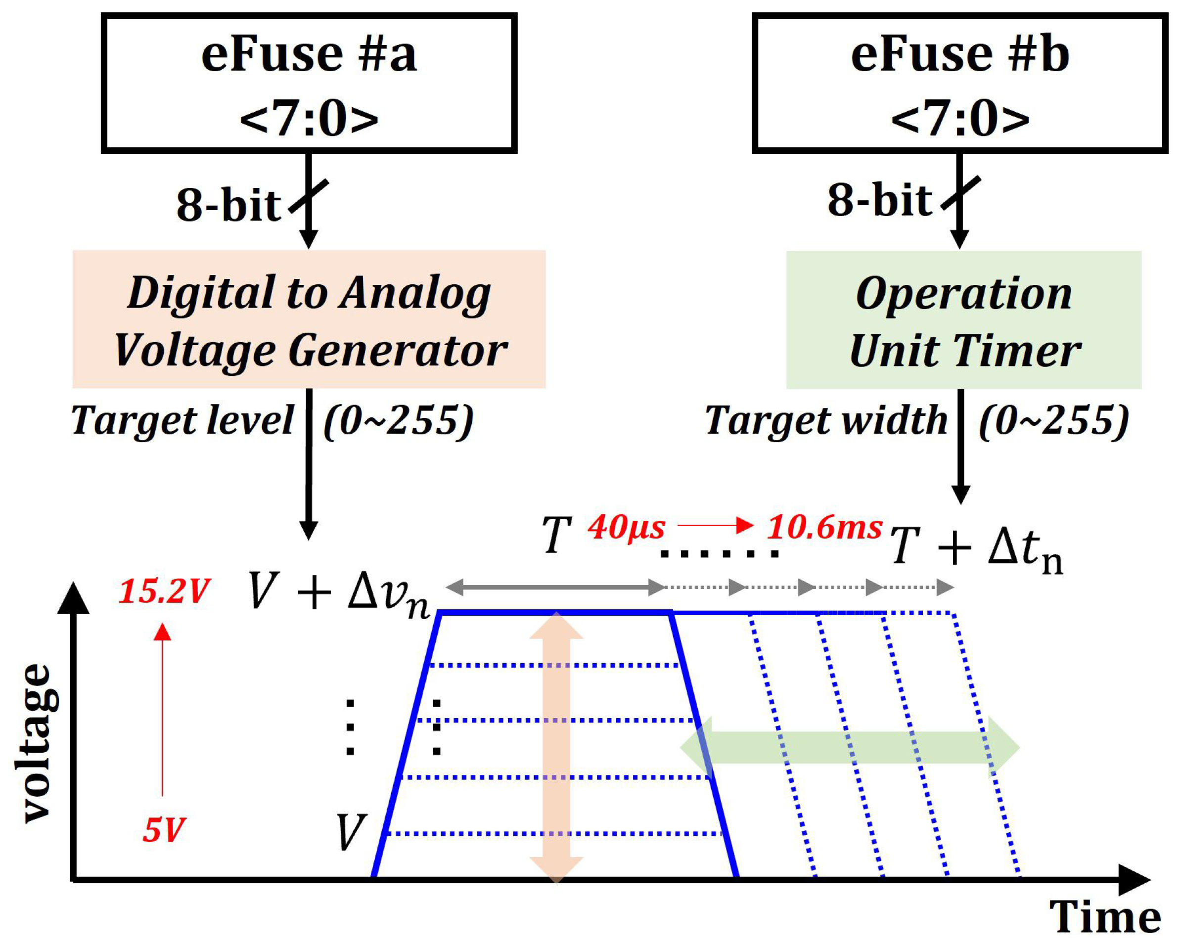
2.2. Tuning NAND Operating Parameter

Just after a NAND flash chip is fabricated, its characteristics are insufficient to work as a commercial memory product. Hence, the internal operating device parameters of NAND flash chips should be carefully tuned to ensure various requirements. Key internal device parameters (e.g., voltage levels or timing values) can be modified by setting a value of electrical fuse (eFuse) that is placed in the peripheral circuit, enabling quick access during NAND operations [20].
Figure 4 shows how internal operating parameters can be tuned using the 8-bit eFuse. The 8-bit eFuse can contain a value from 0 to 255. The analog voltage generator or operation timer circuit is connected to the eFuse, and its corresponding output is determined based on the eFuse’s setting value. For example, when the eFuse value is incremented sequentially from 0 to 255, the analog voltage level output can linearly increase from 5 V to 15.2 V with 40 mV resolution. Similarly, an 8-bit eFuse can change the timing parameter from 40   μ s to 10.6 ms with 40   μ s stepping. As NAND flash memory becomes more advanced, the number of eFuses to be optimized is increasing, so post-fabrication optimization is expected to be more difficult and complex.

3. Overview of NAND Post-Fabrication Optimization

3.1. Example of Post-Fabrication Optimization: Program Operation

Post-fabrication optimization is a key step of the NAND flash manufacturing process to meet various requirements on reliability and performance while maximizing the yield. After fabricating a NAND flash chip, manufacturers should carefully optimize various internal device parameters that determine the target voltage levels and timing values closely related to NAND read/program/erase operations. Each target device parameter value would be stored inside the NAND flash chip using an electrical fuse (eFuse) described in Section 2, and the NAND flash chip performs read/program/erase operations referring to optimized device parameters.
Figure 5 shows how the device parameters for program operation are configured during post-fabrication optimization, which significantly affects the NAND flash chip’s reliability and performance. Modern NAND flash memory commonly adopts the incremental step pulse programming (ISPP) scheme [14] to secure sufficient V t h margins (shown in Figure 2) between adjacent threshold voltage ( V t h ) states (i.e., narrowing the width of each state’s V t h distribution). To maximize V t h margin for flash reliability, the ISPP scheme performs multiple programming steps, gradually increasing the program voltage of each step from V P G M 1 by a certain amount of step voltage Δ V PGM . At the end of each programming step, the ISPP scheme performs verify operations to determine whether target flash cells are programmed sufficiently (i.e., check each cell’s current V t h level). If a cell’s V t h level has sufficiently increased to be higher than the target verify voltage V V F Y i , the ISPP scheme excludes the cell from the next programming steps. Therefore, for optimizing the program operation in NAND flash memory, we need to configure various voltage and timing parameters such as V P G M 1 , Δ V PGM , and V V F Y i .

3.2. Limitation of Conventional Post-Fabrication Optimization

Traditionally, post-fabrication optimization has been done manually by experienced engineers, but doing so becomes highly challenging to modern NAND flash memory for three reasons: (i) increasing device parameters to optimize, (ii) strong process variability, and (iii) limited TAT.
Increasing Parameters. The number of device parameters to optimize for a single NAND flash chip has significantly increased. As NAND flash memory technologies (e.g., 3D stacking or multi-level cell technologies) become more advanced, NAND manufacturers put more device parameters into a NAND flash chip to precisely control each read/program/ erase operation. For example, the number of program-related parameters is around one hundred in triple-level cell (TLC) NAND flash memory, but it increases to more than 2000 in modern quad-level cell (QLC) NAND flash memory. Moreover, these device parameters significantly affect flash reliability and performance in a complex trad-off way. For example, using a smaller Δ V PGM value enables wider V t h margins between adjacent V t h states (i.e., higher reliability), but it leads to a longer program latency (i.e., poor performance).
Process Variability. The strong process variability among 3D flash blocks, which comes from their 3D manufacturing process [21], makes the post-fabrication optimization process more difficult and complex. To evaluate how serious process variability is in 3D NAND flash memory, we performed comprehensive characterization studies using real 160 3D TLC NAND flash memory. In our evaluation, we followed the standard industry practice (i.e., the JEDEC standard [22]), and reliability is measured using an accelerated lifetime test. For example, to emulate a 1-year retention time condition, we baked the flash chips at 85   ° C for 13 h, which is equivalent to one year at 30   ° C based on Arrhenius’s law [23].
As shown in Figure 6a, our characterization study reveals that there are considerable variations in lifetime over different blocks. Furthermore, as shown in Figure 6b, even within a single block, there are large variations in the bit error rates (RBER, Row Bit Error Rates) among different WLs in the block. For example, even in the same operating condition, the RBER of the worst WL exceeds 2.25 times more than that of the best WL. Therefore, manual-based post-fabrication optimization for all different chips, blocks, and WLs is no longer practical in modern 3D NAND flash memory.
Limited TAT. The post-fabrication optimization is a time-critical process. The turnaround time (TAT), i.e., the total amount of time taken to complete the production of new NAND flash chips, is quite limited for developing a new generation of NAND flash memory. As the TAT includes the time for not only post-fabrication optimization but also many other tasks, e.g., the layout design, fabrication, and verification of chips, only a week or even fewer days are given for post-fabrication optimization in many cases. Manually optimizing a large number of parameters within such a limited time requires significant human effort and fails to achieve near-optimal results.

4. HAIPO: Hybrid AI Algorithm-Based Post-Fabrication Optimization

This section introduces a new optimization system, HAIPO, that efficiently exploits the AI algorithm for NAND post-fabrication optimization. The key idea of our HAIPO is to automatically search and find the optimal eFuse configuration based on deep learning (DL) and rule-based evolutionary algorithm (EA) with three guidelines. Since our work is the first attempt to automate post-fabrication optimization of NAND flash memory, we develop our technique using a well-known deep-learning model and evolutionary algorithm. (In the future, we plan to evaluate more advanced and various deep-learning models and algorithms to better optimize our work.) First, to develop HAIPO efficiently, we design a 2-phase framework for a machine-learning-based optimization system called HAIPO(-). Second, to further optimize HAIPO(-), we add three guidelines for each generation in EA to complete the final technique, HAIPO. Since three guidelines in EA can effectively reduce the eFuse configuration to be measured, we can evaluate a large number of populations within the limited measurement times, accelerating the entire post-optimization process. Finally, we integrate two additional optimization modules with our technique: one aims to improve the robustness by considering process variability in a 3D NAND flash chip, and the other enhances optimization TAT in an environment where multiple requirements must be satisfied simultaneously.

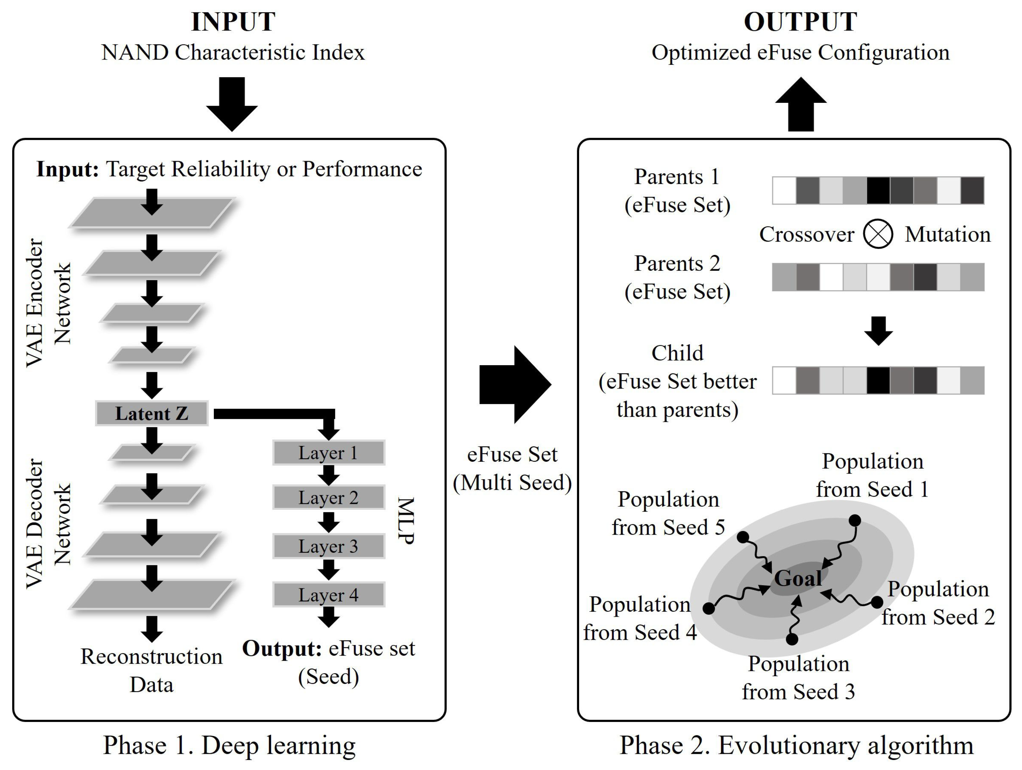
4.1. 2-Phase Framework for a Machine-Learning-Based Optimization, HAIPO(-)

Figure 7 illustrates the overall procedure of how HAIPO(-) works. In the first phase, the DL model generates initial device parameters that can roughly meet the given performance and reliability requirements. The engineer decides the values of target characteristic indices (e.g., reliability and performance requirements) and applies them to the input of DL networks. HAIPO(-) uses (i) a variational autoencoder (VAE) to encode the performance and reliability characteristics of target chips into latent values to reduce the dimension of eFuse searching and (ii) a Multi-Layer Perceptron (MLP) to generate initial device parameters (i.e., eFuse configurations) from the latent values. To reduce the eFuse dimension, instead of using a general autoencoder, HAIPO(-) employs VAE to create new data similar to the input characteristics [24]. By doing so, we can effectively avoid unexpected inputs given to the model due to the complex physics of NAND flash memory and can design a more flexible DL model [25]. HAIPO(-) also adopts the Multi-Layer Perceptron (MLP), a fully connected structure, to connect the latent z layer of the VAE with eFuses value [26]. Given the inputs, MLP creates the eFuse combinations that are expected to achieve target characteristics. In conclusion, the DL is a generative model that transforms NAND characteristic data into latent z and makes eFuses configuration using the transformed latent z. The eFuses configuration generated through this process is called a seed, and DL creates several types of seeds and delivers them to the second phase.
In the second phase, the EA performs parameter exploration from the initial values by repeating (i) random mutation/crossover on the previous populations and (ii) evaluation of new populations on target chips. The EA terminates the exploration either when the given time for post-fabrication optimization is over or when it finds a parameter set that can meet all requirements. The EA progressively optimizes device parameters immediately using each real-device measurement, therefore increasing the possibility of finding the optimal eFuse configuration for the target NAND flash chip.

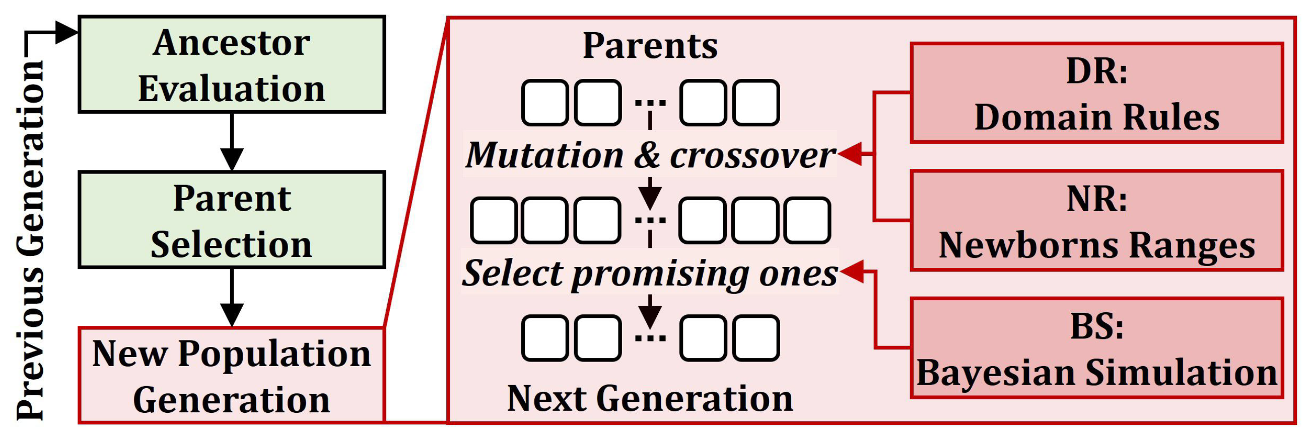
4.2. Rule-Based EA, HAIPO

The key idea of this technique is to efficiently generate the device parameters for each generation in the EA so that more promising parameters can be tested on real chips. Doing so can accelerate the entire optimization process and maximize the optimization level.
Figure 8 shows how HAIPO generates the next-generation populations from the previous populations called ancestors. The overall procedure of HAIPO is similar to a typical EA’s process that consists of three steps: (i) ancestor evaluation, (ii) parent selection, and (iii) new population generation. The first two steps are simple; HAIPO first calculates each ancestor’s achievement score that indicates how well the ancestor’s device parameters meet the performance/reliability requirements and then selects the high-score parents for generating a new population. In the third step, HAIPO effectively explores a large number of populations using three guides, i.e., DR, NR, and BS, along with random mutation and crossover. The first guide, DR, sets the conditions that every population should satisfy, which can be obtained from domain-specific knowledge. The second guide, NR, specifies a suitable range for every parameter based on the recent populations with high achievement scores. The third guide, BS, predicts the achievement score of each candidate population (generated by random mutation and crossover with the other two guides) using Bayesian simulation and selects the ones with the highest simulated scores as the next generation. In the following sections, we provide more details about the overall steps of rule-based EA and three guidelines.

4.2.1. Ancestor Evaluation and Parent Selection

For each ancestor A i that consists of N device parameter values { a 0 , a 1 , …, a N 1 }, HAIPO characterizes target NAND flash chips using the ancestor’s device parameters and an object function that calculates the achievement score S i as follows:
S i = k = 0 M 1 w k × m k ( A i ) ,
where m k is k-th evaluation metric (total M metrics), and w k is the corresponding weight. Examples of m k include (i) VSum (the total margins between every two adjacent V t h states), (ii) Disturb (the maximum V t h level of erased cells after programming), and (iii) tPROG (the average program latency), all of which can be obtained via real-device measurements with each ancestor A i . After measuring m k ( A i ) values for all metrics and ancestors, HAIPO calculates an ancestor’s benefit for each metric by multiplying the predefined w k ; if a lower value is preferable (e.g., Disturb and tPROG), the weight is negative value; if a higher value is preferable (e.g., VSum), the weight is positive value. Finally, HAIPO adds up all benefits as the ancestor’s achievement score (the higher the score, the better). And then, the ancestors with the best scores are chosen to be the parents of the following generation.

4.2.2. New Population Generation

HAIPO generates new populations using three key guidelines that enable efficient finding of optimal parameters across candidates.
Guideline 1. DR: Domain Rules. DR specifies the necessary conditions, called domain rules, that certain device parameters should not violate in any crossover and mutation process. Domain rules are predefined by experienced engineers using domain-specific knowledge. Based on the NAND flash memory physics, highly correlated device parameters and their effect on reliability/performance are well known. As shown in Section 3, the range of program-related device parameters such as Δ V PGM or V V F Y i is quite limited in terms of performance and reliability tread-off relationships. For example, if the target tPROG is less than 1 ms, DR can specify that Δ V PGM cannot exceed 50 mV. Therefore, among the populations generated by the EA algorithm, eFuse combinations with Δ V PGM exceeding 50 mV are considered unnecessary populations that cannot be used for optimization and are eliminated from the new population candidates. Similarly, if you remember V V F Y i is used for checking a cell’s V t h level during each program step, we can easily extract DR for V V F Y i that V V F Y i must be lower than V V F Y j if i < j . In conclusion, DR prevents the scarce real-device measurements from being wasted for unrealistic values that violate the basic properties but can be generated by random mutation and crossover. In our HAIPO, we use five key domain rules closely related to ∼600 device parameters.
Guideline 2. NR: Newborns Ranges. NR specifies desired ranges of certain parameters of the new populations, called newborn ranges, based on the device parameters of ancestors that record the highest achievement scores. To efficiently implement NR, HAIPO maintains greatest ancestors list (GAList) that stores a fixed number of ancestors with the highest achievement scores until the current iteration. For each device parameter, HAIPO searches the corresponding Min./Max. values in GAList among the ones that satisfy all the related domain rules. It enables the EA to (i) avoid generating undesirable values for highly correlated parameters and (ii) find near-optimal parameters more rapidly by updating GAList every iteration, which leads to the highest achievement scores (i.e., it reinforces the desired ranges every iteration).
Figure 9 shows an example of how HAIPO generates new populations using domain rules and newborn ranges. In this example, HAIPO determines the k-th device parameter, V V F Y 3 , from P x and P y that is selected as the parent. HAIPO performs either mutation that generates a random value at a very low probability μ or crossover that selects one of the corresponding values from the parent at a probability of ( 1 μ ). In both cases, HAIPO identifies all domain rules related to the device parameter, e.g., V V F Y 3 > V V F Y 2 . For mutation, HAIPO repeats random number generation until the value meets all the related domain rules (Case 1 in Figure 9). For crossover, HAIPO uses the new value only if the value meets all the related newborn ranges as well as all the related domain rules (Case 2-1). As shown in Figure 9, HAIPO derives a newborn range for V V F Y 3 when V V F Y 2 = 1 V, e.g., 1.2 ≤ V V F Y 3 ≤ 2, based on the Min./Max. values for V V F Y 3 when V V F Y 2 = 1 V in GAList (Case 2-2). If the new crossover value for V V F Y 3 violates any domain rules and newborn ranges, HAIPO randomly selects a value in the newborn ranges.
Guideline 3. BS: Bayesian Simulation. We start developing our technique using a well-known Bayesian simulation to reduce the time-consuming real-device measurements for calculating the achievement score. BS effectively alleviates the inherent bottleneck in the post-fabrication optimization by predicting the achievement score of each new population generated by EA based on two guidelines, DR and NR. The entire time for post-fabrication optimization is determined by the time-consuming real-device measurements required to obtain the achievement score. For example, even though DR and NR effectively generate promising populations, only a fixed number of populations can be explored because the capability of real-device measurements within the given time is quite limited. To explore more populations within the limited time, BS performs a simple simulation using a Bayesian model to estimate a population’s achievement score.
Figure 10 depicts how HAIPO decides the final next-generation populations. BS maintains a Bayesian model throughout the optimization process, which takes a population (i.e., a set of device parameters) as input and returns the estimated achievement score of the population as output. For the ancestors in the previous generation (the initial parameter sets for the first generation), BS updates the Bayesian model (i.e., (re)training) by feeding each ancestor A i along with its achievement score S i calculated based on real-device measurement results as described in Equation (1). Then, once a new population is generated via mutation and crossover with the other two guides, BS performs inference using the Bayesian model that estimates the new population’s achievement score without real-device measurements. Finally, HAIPO selects the new populations with the highest estimated scores as the ancestors for the next generation.
Since BS can rapidly perform the Bayesian simulation for a candidate, HAIPO can explore much more candidate populations than real-device measurements. For example, it takes ∼100 min per iteration to generate/test all populations on real-device measurement for 400 ancestors per generation, whereas ∼1000 candidate populations can be simulated within 1 min. Details of our Bayesian simulation are summarized in Table 1.

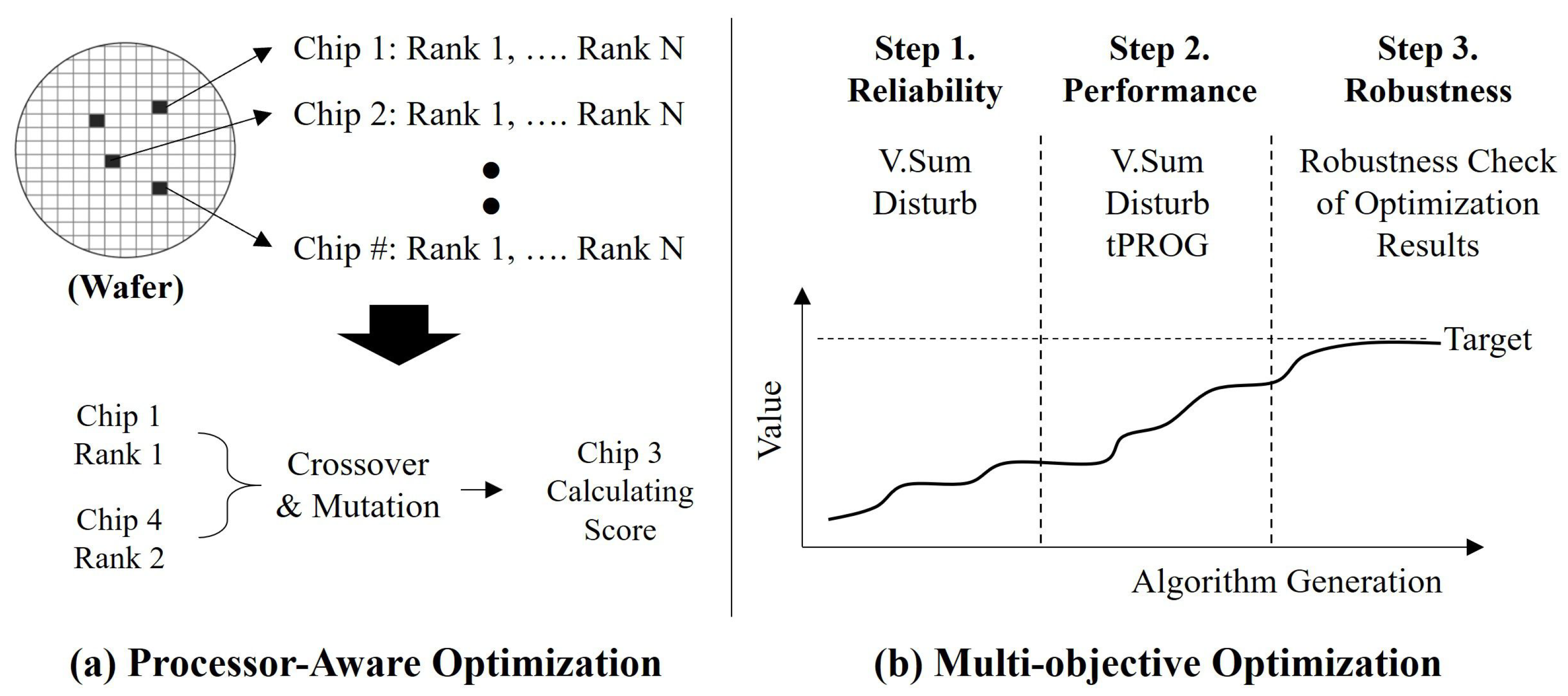
4.3. Additional Optimization Modules: Process-Aware and Multi-Objective Optimization
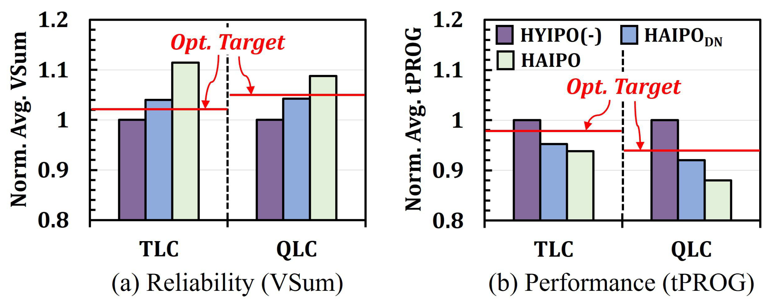
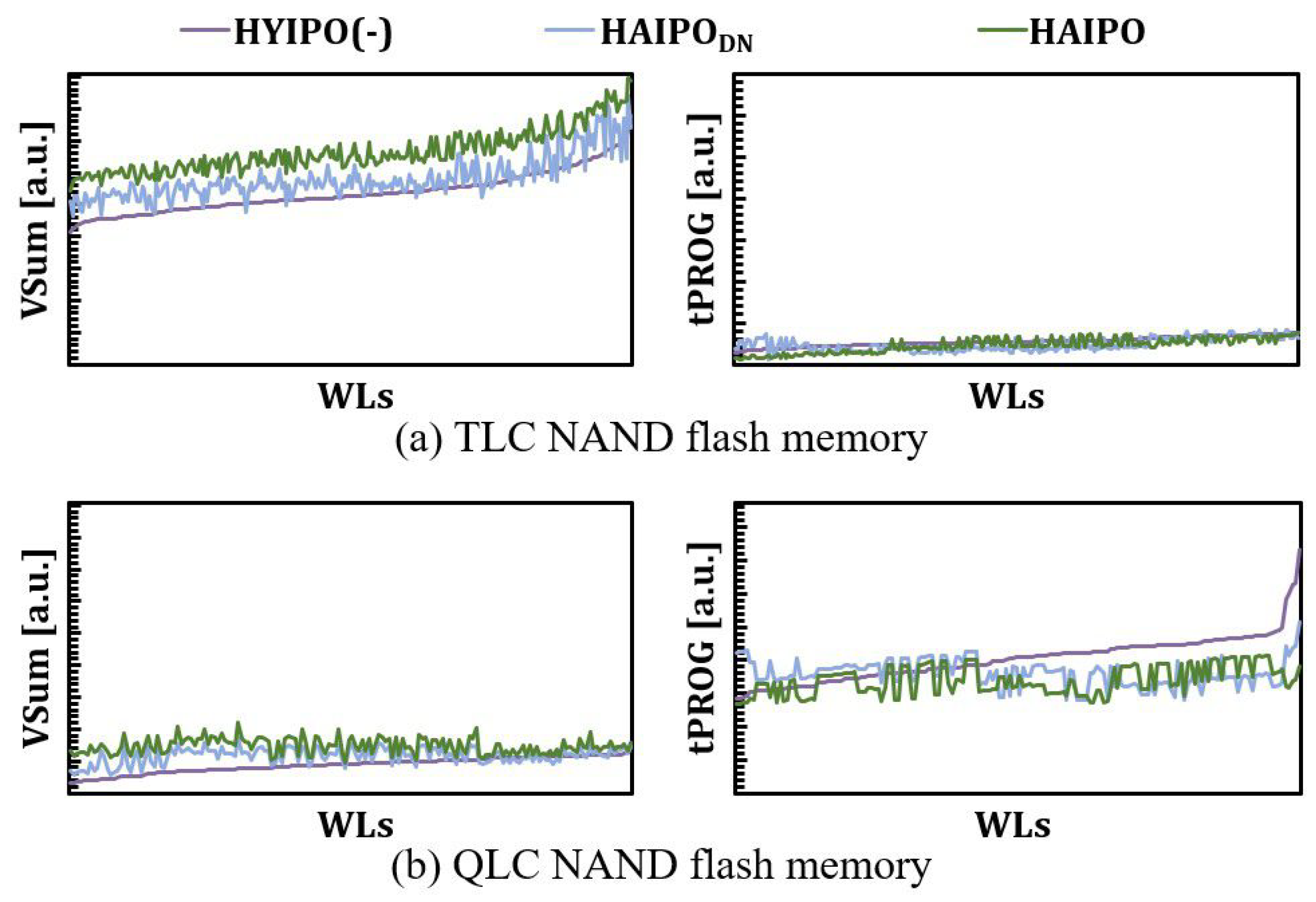
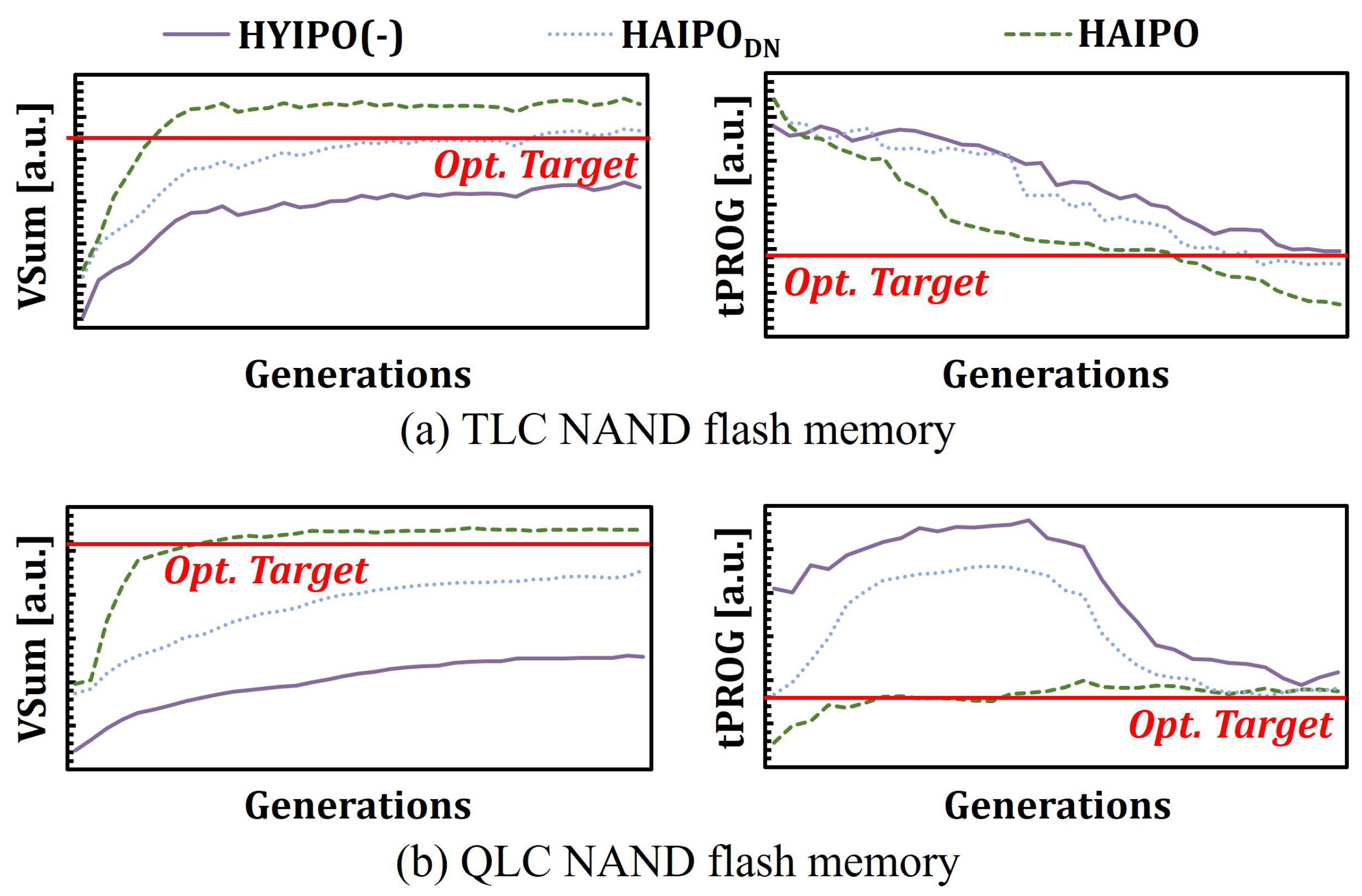
To further improve the entire optimization process, we devise two modules and integrate them with our HAIPO: (i) process-aware optimization and (ii) multi-objective optimization.
Process-Aware Optimization. As explained in Section 3, strong process variability originating from the 3D manufacturing process results in different characteristics of NAND flash chips even in the same eFuse configuration, thus increasing the complexity of post-fabrication optimization. Due to process variability, even NAND flash chips within the same wafer can exhibit different performance and reliability. (NAND flash memory is fabricated on the wafer, and more than hundreds of NAND flash chips are produced in a single wafer.) Moreover, blocks within a single NAND flash chip and WLs in a block also represent different characteristics. Therefore, achieving the global optimal eFuse configuration for different NAND flash chips becomes more challenging. To address such challenges, we introduce process-aware optimization that efficiently compensates for a noise factor from process variability. Figure 11a illustrates the basic concept of process-aware optimization technique. For individual NAND flash chips, the EA calculates the achievement score and ranks the score of each eFuse configuration. The EA selects two eFuse configurations from different NAND flash chips and generates a new population through the crossover and mutation. The EA evaluates the achievement score of a new population in different NAND flash chips and repeats this procedure for all generations to obtain the effect of circulating eFuse configurations on all NAND flash chips. By doing so, our HAIPO efficiently achieves global optimization for all target NAND flash chips with different characteristics.
Multi-objective Optimization. Various objectives (i.e., requirements) should be satisfied in our optimization process. However, as the number of objectives increases, the total time for optimization becomes longer. To efficiently optimize multiple objectives, HAIPO introduces an adaptive fitness function that performs optimization by flexibly changing the target objectives instead of optimizing all objectives simultaneously. As shown in Figure 11b, HAIPO selects reliability objectives in the initial step. It gradually expands the target objectives by adding performance in the mid-step and robustness in the final step. This approach makes our HAIPO reduce the optimization TAT efficiently (e.g., by up to 20%).

5. Evaluation

Methodology. We validate our HAIPO using two types of 320ea modern 3D NAND flash chips: (i) 3D TLC NAND flash chips and (ii) the 3D QLC NAND flash chips. To investigate the effectiveness of BS (Bayesian simulation), we also evaluate the optimization using only DR and NR (HAIPODN). For each type of chip, we perform post-fabrication optimization using one of HAIPO, HAIPODN, and HAIPO(-) on 40 blocks in 320 NAND flash chips that are randomly selected from different locations. After post-fabrication optimization, we evaluate the final reliability and performance of the selected NAND flash chips with the device parameters obtained from the three techniques. All test procedures for reliability and performance follow commercial industry standards [22].
Since our proposed technique is the first attempt to automatically explore the optimal eFuse combination to satisfy various memory requirements such as reliability and performance, it is challenging to compare the results of our technique with those of other prior works with the same research goal. Therefore, the effectiveness of our work is verified across different steps in implementing our technique.
Reliability and Performance. Figure 12 compares the reliability and performance of the three post-fabrication optimization techniques in the TLC and QLC NAND flash chips. We measure VSum (the higher, the better) and average program latency tPROG (the lower, the better), respectively.
We make two observations from Figure 12. First, HAIPO significantly improves reliability by 11% (8.8%) and performance by 6.2% (12%) on average for the TLC (QLC) NAND flash chips compared to HAIPO(-). The performance and reliability benefits clearly show the effectiveness of HAIPO at optimizing device parameters that are hard to find in manual-based optimization. Second, BS (Bayesian simulation) is the key factor for HAIPO to meet the reliability requirement in modern NAND flash memory. HAIPODN also provides considerable benefits over HAIPO(-) (4.1% and 6.4% in reliability and performance, respectively, on average) but still fails to satisfy the reliability requirement in QLC NAND flash chips. This clearly shows that the Bayesian simulation plays a critical role in improving the effectiveness of our HAIPO.
To further confirm the advantage of HAIPO on reliability, we investigate the V t h distribution in TLC NAND flash chips. As shown in Figure 13, HAIPO improves the reliability over HAIPO(-) significantly, resulting in (i) narrower distribution of all V t h states (i.e., improving VSum) and (ii) improving the amount of Disturb in the erased cells (i.e., lowering the RBERs).
In addition, to assess the efficiency of HAIPO, we examine how well our technique optimizes reliability and performance across generations. Figure 14 shows the change in reliability and performance of 3D TLC NAND flash memory according to the generations. The blue dots indicate the results of individual eFuses configurations, and the red solid line represents the center value of reliability and performance. In the initial step, VSum values are very widely distributed because a large number of eFuse configurations are examined. In the mid-step, the variation of the VSum values is shrunk, and the slope of the optimization gradually decreases. From the results, we can identify that if we aim to further optimize our HAIPO, we should focus on improving the optimization speed in the mid and final steps of our technique.
Per-WL Optimization. To better understand the effectiveness of HAIPO, we analyze the reliability and performance across different WLs. Figure 15 shows the average VSum (the larger, the better reliability) and tPROG (the lower, the better performance) of each WL in a 3D TLC/QLC NAND flash block. To simplify the results, we sort the WLs in ascending order according to the VSum and tPROG values. As shown in Figure 15, HAIPO enhances reliability over HAIPO(-) for all WLs in both TLC and QLC NAND flash chips. In addition, we can also identify that HAIPO significantly improves the performance of the worst WLs in a block (i.e., lower the tPROG difference between the best and worst WL). Uniform tPROG between WLs is important because deterministic I/O performance is increasingly critical in various modern data-intensive applications [27,28].
Optimization TAT. Finally, we compare the optimization speeds of the three techniques. Figure 16 shows how the three evaluated techniques improve the reliability (left) and performance (right) over time (until 100 generations) for the TLC and QLC NAND flash chips. Please note that all three techniques terminate post-fabrication optimization when all requirements are met or when the given time (e.g., 100 generations) is over. From the evaluation results, we observe that HAIPO significantly accelerates the entire optimization process over HAIPO(-). HAIPO can improve the reliability close to the optimization target within less than 30 generations, while HAIPO(-) fails to achieve the target reliability until 100 generations. We also observe that Bayesian simulation critically impacts the optimization TAT. At the 50th generation for the QLC NAND flash chips, HAIPO meets both the reliability and performance requirements, but the reliability and performance levels achieved by HAIPODN are quite far from the optimization target.
Figure 17 shows the comparison of the optimization TAT of different techniques in optimizing real 3D TLC NAND flash chips. HAIPO efficiently reduces the total optimization TAT up to 70% compared with the manual-based optimization. As mentioned above, it is not easy to find other research work to be compared with our technique. Therefore, we compare the effectiveness of our work with the conventional manual-based approach. We obtained the optimization TAT of the manual-based approach from two representative NAND manufacturers. Based on our evaluation results and observations, we conclude that HAIPO is an effective post-fabrication optimization method for modern 3D NAND flash memory.

6. Related Work

To our knowledge, our work is the first to propose an automatic post-fabrication optimization technique that provides significant benefits in advanced NAND flash memory. In this section, we briefly describe other techniques closely related to our work.
Post-Fabrication Optimization of NAND Flash Memory. Several other studies have also attempted to automate the optimization process of NAND flash memory. Bongale et al. [29] and Xanthopoulos et al. [30] propose techniques that optimize individual parameters of analog circuits in NAND flash memory. The proposed techniques achieve better eFuse values by considering inter-chip variations during post-fabrication optimization. However, previous studies still require a great deal of human effort compared to automatic post-fabrication optimization approaches and are difficult to address complex dependencies between device parameters.
Turnaround Time (TAT) Optimization. Recent researchers have attempted to reduce post-fabrication test time for integrated circuits using neural networks or genetic algorithms (GAs) to reduce TAT. Golonek et al. [31] have explored the optimal test points using a GA-based approach. Lin et al. [32] introduced an autoencoder (AE)-based methodology for test screening escape. Shintani et al. [33] introduced an outlier screening method for test escape using a variational autoencoder (VAE) that can avoid the potential risk of overfitting by extracting training data features as a probability distribution. HAIPO also adopts similar approaches (e.g., VAE and GAs) to enable rapid yet efficient post-fabrication optimization of modern NAND flash memory.

7. Conclusions

We propose HAIPO, a new post-fabrication optimization method for modern NAND flash memory that meets the target reliability and performance requirements within a limited optimization TAT. HAIPO successfully automates a complex (i.e., a huge number of highly correlated device parameters and strong process variability) and time-consuming optimization process by efficiently exploiting deep learning and evolutionary algorithms. HAIPO fundamentally addresses the key limitations of conventional manual-based optimization, i.e., being bottlenecked by real-device measurements, by providing three key guidelines that effectively accelerate the optimization process. We experimentally demonstrate the effectiveness of HAIPO using real TLC/QLC NAND flash chips, showing its high advantages in reliability and performance optimization.
We will extend our model in two directions. First, we plan to develop the post-fabrication optimization using more advanced machine-learning models and algorithms such as bio-inspired metaheuristics. Since our work is the first attempt to automate post-fabrication optimization, we design our technique using the most well-known algorithms. In the future, we will explore various algorithms that can better reflect the domain-specific characteristics of NAND flash memory. Second, we also plan to extend our model by constructing a meta-model. We will further improve the model’s predictive power by combining our work with a Bayesian-based probability estimation model and a tree structure model.

Funding

This research was supported by IITP (Institute for Information & Communication Technology Planning & Evaluation) (RS-2024-00347394), National Research Foundation of Korea (NRF) grant funded by the Korea government (MSIT) (RS-202400414964), and MOTIE (Ministry of Trade, Industry and Energy) (1415181081), KSRC (Korea Semiconductor Research Consortium) (20019402).

Data Availability Statement

The data presented in this study are available on request from the corresponding author. The data are not publicly available due to an NDA with the NAND manufacturer.

Acknowledgments

The support from the School of Computer Science and Engineering, Kyungpook National University, is appreciated.

Conflicts of Interest

The authors declare no conflicts of interest.

References

  1. Samsung. Samsung Enterprise SSDs. 2023. Available online: https://semiconductor.samsung.com/ssd/enterprise-ssd (accessed on 21 November 2024).
  2. SK Hynix. SK Hynix Enterprise SSDs. 2023. Available online: https://product.skhynix.com/products/ssd/essd.go (accessed on 21 November 2024).
  3. Micron. Micron Enterprise SSDs. 2023. Available online: https://www.micron.com/products/ssd/product-lines/9400 (accessed on 21 November 2024).
  4. Western Digital. Western Digital Data Center SSDs. 2023. Available online: https://github.com/axboe/fio (accessed on 21 November 2024).
  5. LeCun, Y.; Bengio, Y.; Hinton, G. Deep learning. Nature 2015, 521, 436–444. [Google Scholar] [CrossRef] [PubMed]
  6. Whitley, D. A genetic algorithm tutorial. Stat. Comput. 1994, 4, 65–85. [Google Scholar] [CrossRef]
  7. Maserjian, J.; Zamani, N. Behavior of the Si/SiO2 interface observed by Fowler-Nordheim tunneling. J. Appl. Phys. (JAP) 1982, 53, 559–567. [Google Scholar] [CrossRef]
  8. Kim, D.; Kim, H.; Yun, S.; Song, Y.; Kim, J.; Joe, S.M.; Kang, K.H.; Jang, J.; Yoon, H.J.; Lee, K.; et al. 13.1 A 1 Tb 4b/cell NAND Flash Memory with tPROG = 2 ms, tR = 110 µs and 1.2 Gb/s High-Speed IO Rate. In Proceedings of the International Solid-State Circuits Conference (ISSCC), San Francisco, CA, USA, 16–20 February 2020. [Google Scholar]
  9. Kim, M.; Yun, S.W.; Park, J.; Park, H.K.; Lee, J.; Kim, Y.S.; Na, D.; Choi, S.; Song, Y.; Lee, J.; et al. A 1 Tb 3b/Cell 8th-Generation 3D-NAND Flash Memory with 164 MB/s Write Throughput and a 2.4 Gb/s Interface. In Proceedings of the International Solid-State Circuits Conference (ISSCC), San Francisco, CA, USA, 20–26 February 2022. [Google Scholar]
  10. Cho, J.; Kang, D.C.; Park, J.; Nam, S.-W.; Song, J.-H.; Jung, B.-K.; Lyu, J.; Lee, H.; Kim, W.-T.; Jeon, H.; et al. 512 Gb 3b/Cell 7th-Generation 3D-NAND Flash Memory with 184 MB/s Write Throughput and 2.0 Gb/s Interface. In Proceedings of the International Solid-State Circuits Conference (ISSCC), San Francisco, CA, USA, 13–22 February 2021. [Google Scholar]
  11. Kanda, K.; Shibata, N.; Hisada, T.; Isobe, K.; Sato, M.; Shimizu, Y.; Shimizu, T.; Sugimoto, T.; Kobayashi, T.; Kanagawa, N.; et al. A 19 nm 112.8 mm2 64 Gb Multi-Level Flash Memory with 400 Mbit/sec/pin 1.8 V Toggle Mode Interface. IEEE J. Solid-State Circuits (JSSC) 2012, 64, 426–428. [Google Scholar] [CrossRef]
  12. Kim, M.; Chun, M.; Hong, D.; Kim, Y.; Cho, G.; Lee, D.; Kim, J. RealWear: Improving performance and lifetime of SSDs using a NAND aging marker. Perform. Eval. 2021, 48, 120–121. [Google Scholar] [CrossRef]
  13. Micheloni, R.; Crippa, L.; Marelli, A. Inside NAND Flash Memories; Springer: Dordrecht, The Netherlands, 2010. [Google Scholar] [CrossRef]
  14. Suh, K.; Suh, B.-H.; Lim, Y.-H.; Kim, J.-K.; Choi, Y.-J.; Koh, Y.-N.; Lee, S.-S.; Kwon, S.-C.; Choi, B.-S.; Choi, J.-H.; et al. A 3.3 V 32 Mb NAND Flash Memory with Incremental Step Pulse Programming Scheme. IEEE J. Solid-State Circuits (JSSC) 1995, 30, 1149–1156. [Google Scholar]
  15. Kim, M.; Song, Y.; Jung, M.; Kim, J. SARO: A State-Aware Reliability Optimization Technique for High Density NAND Flash Memory. In Proceedings of the Great Lakes Symposium on VLSI (GLSVLSI), Chicago, IL, USA, 23–25 May 2018. [Google Scholar] [CrossRef]
  16. Jung, S.M.; Jang, J.; Cho, W.; Cho, H.; Jeong, J.; Chang, Y.; Kim, J.; Rah, Y.; Son, Y.; Park, J.; et al. Three dimensionally stacked NAND flash memory technology using stacking single crystal Si layers on ILD and TANOS structure for beyond 30 nm node. In Proceedings of the International Electron Devices Meeting (IEDM), San Francisco, CA, USA, 11–13 December 2006. [Google Scholar]
  17. Micron. Micron’s 232 Layer NAND Now Shipping: 1Tbit, 6-Plane Dies with 50% More I/O Bandwidth. 2020. Available online: https://www.anandtech.com/show/17509 (accessed on 21 November 2024).
  18. Jang, J.; Kim, H.-S.; Cho, W.; Cho, H.; Kim, J.; Shim, S.I.; Younggoan; Jeong, J.-H.; Son, B.-K.; Kim, D.W.; et al. Vertical cell array using TCAT (Terabit Cell Array Transistor) technology for ultra high density NAND flash memory. In Proceedings of the Symposium on VLSI Technology, Kyoto, Japan, 15–17 June 2009. [Google Scholar]
  19. Kim, B.; Seo, G.; Kim, M. Smart Electrical Screening Methodology for Channel Hole Defects of 3D Vertical NAND (VNAND) Flash Memory. Eng 2024, 5, 495–512. [Google Scholar] [CrossRef]
  20. Robson, N.; Safran, J.; Kothandaraman, C.; Cestero, A.; Chen, X.; Rajeevakumar, R.; Leslie, A.; Moy, D.; Kirihata, T.; Iyer, S. Electrically Programmable Fuse (eFuse): From Memory Redundancy to Autonomic Chips. In Proceedings of the IEEE Custom Integrated Circuits Conference (CICC), San Jose, CA, USA, 16–19 September 2007. [Google Scholar]
  21. Shim, Y.; Kim, M.; Chun, M.; Park, J.; Kim, Y.; Kim, J. Exploiting Process Similarity of 3D Flash Memory for High Performance SSDs. In Proceedings of the IEEE/ACM International Symposium on Microarchitecture (MICRO), Columbus, OH, USA, 12–16 October 2019. [Google Scholar] [CrossRef]
  22. JEDEC. JESD218B.02: Solid-State Drive (SSD) Requirements and Endurance Test Method. 2022. Available online: https://www.jedec.org/standards-documents/docs/jesd218b01 (accessed on 21 November 2024).
  23. Arrhenius, S. Über die Dissociationswärme und den Einfluss der Temperatur auf den Dissociationsgrad der Elektrolyte. Z. Phys. Chem. 1889, 4, 96–116. [Google Scholar] [CrossRef]
  24. Hou, X.; Shen, L.; Sun, K.; Qiu, G. Deep feature consistent variational autoencoder. In Proceedings of the IEEE Winter Conference on Applications of Computer Vision (WACV), Santa Rosa, CA, USA, 24–31 March 2017. [Google Scholar] [CrossRef]
  25. Lim, K.L.; Jiang, X.; Yi, C. Deep clustering with variational autoencoder. IEEE Signal Process. Lett. 2020, 27, 231–235. [Google Scholar] [CrossRef]
  26. Kim, J.; Lee, J.; Yoo, S. Machine Learning-Based Automatic Generation of eFuse Configuration in NAND Flash Chip. In Proceedings of the IEEE International Test Conference (ITC), Washington, DC, USA, 9–15 November 2019. [Google Scholar] [CrossRef]
  27. Li, H.; Putra, M.L.; Shi, R.; Lin, X.; Ganger, G.R.; Gunawi, H.S. IODA: A Host/Device Co-Design for Strong Predictability Contract on Modern Flash Storage. In Proceedings of the ACM SIGOPS 28th Symposium on Operating Systems Principles (OSDI), Virtual, 26–29 July 2021. [Google Scholar] [CrossRef]
  28. Kim, S.; Yang, J.S. Optimized I/O Determinism for Emerging NVM-based NVMe SSD in an Enterprise System. In Proceedings of the Annual Design Automation Conference (DAC), San Francisco, CA, USA, 24–29 June 2018. [Google Scholar] [CrossRef]
  29. Bongale, P.; Sundaresan, V.; Ghosh, P.; Parekhji, R. A Novel Technique for Interdependent Trim Code Optimization. In Proceedings of the IEEE VLSI Test Symposium (VTS), Las Vegas, NV, USA, 25–27 April 2016. [Google Scholar]
  30. Xanthopoulos, C.; Ahmadi, A.; Boddikurapati, S.; Nahar, A.; Orr, B.; Makris, Y. Wafer-Level Adaptive Trim Seed Forecasting Based on E-Tests. In Proceedings of the IEEE International Symposium on Circuits and Systems (ISCAS), Baltimore, MD, USA, 28–31 May 2017. [Google Scholar]
  31. Golonek, T.; Rutkowski, J. Genetic-Algorithm-Based Method for Optimal Analog Test Points Selection. IEEE Trans. Circuits Syst. II Express Briefs (TCAS-II) 2007, 54, 117–121. [Google Scholar] [CrossRef]
  32. Lin, F.; Cheng, K.T. An Artificial Neural Network Approach for Screening Test Escapes. In Proceedings of the Asia and South Pacific Design Automation Conference (ASP-DAC), Tokyo, Japan, 16–19 January 2017. [Google Scholar]
  33. Shintani, M.; Inoue, M.; Nakamura, Y. Artificial Neural Network Based Test Escape Screening Using Generative Model. In Proceedings of the IEEE International Test Conference (ITC), Phoenix, AZ, USA, 29 October–1 November 2018. [Google Scholar]
Figure 1. An organizational overview of NAND flash memory.
Processes 12 02760 g001
Figure 2. V t h distributions of 2 m -state NAND flash memory.
Processes 12 02760 g002
Figure 3. Illustration of organizational difference between 2D and 3D NAND flash memory.
Processes 12 02760 g003
Figure 4. Overview of NAND eFuse operation.
Processes 12 02760 g004
Figure 5. ISPP mechanism and related operating parameters.
Processes 12 02760 g005
Figure 6. Reliability variation in 3D NAND flash memory.
Processes 12 02760 g006
Figure 7. Overall procedure of the 2-phase framework for a machine-learning-based optimization.
Processes 12 02760 g007
Figure 8. Overview of optimization process in HAIPO.
Processes 12 02760 g008
Figure 9. Generation of a new population in HAIPO.
Processes 12 02760 g009
Figure 10. Decision of final populations with the Bayesian model.
Processes 12 02760 g010
Figure 11. Additional optimization modules: (a) Process-aware individual chip optimization, (b) Multi-objective optimization using an adaptive fitness function.
Processes 12 02760 g011
Figure 12. Reliability (VSum) and performance (tPROG) comparisons of three post-fabrication optimization techniques for the TLC and QLC NAND flash chips.
Processes 12 02760 g012
Figure 13. Comparison of V t h distributions in TLC 3D NAND flash memory across three post-fabrication optimization techniques.
Processes 12 02760 g013
Figure 14. Optimization behavior on reliability and performance.
Processes 12 02760 g014
Figure 15. Reliability and performance across WLs for TLC and QLC 3D NAND flash chips.
Processes 12 02760 g015
Figure 16. Optimization speed comparison for TLC and QLC 3D NAND flash chips.
Processes 12 02760 g016
Figure 17. Optimization speed comparison for HAIPO and QLC 3D NAND flash chips.
Processes 12 02760 g017
Table 1. Details of Bayesian simulation.
ModelSklearn GPR (Gaussian Process Regressor)
KernelRadial Basis Function Kernel + Constant Kernel
NormalizationStandard Scaling
Disclaimer/Publisher’s Note: The statements, opinions and data contained in all publications are solely those of the individual author(s) and contributor(s) and not of MDPI and/or the editor(s). MDPI and/or the editor(s) disclaim responsibility for any injury to people or property resulting from any ideas, methods, instructions or products referred to in the content.

