Review

Recent Progress in Surface Acoustic Wave Sensors Based on Low-Dimensional Materials and Their Applications

1
Yangtze Delta Region Institute (Huzhou), University of Electronic Science and Technology of China, Huzhou 313001, China
2
Ningbo Research Institute of Ecological and Environmental Sciences, Ningbo 315000, China
3
School of Science, Wuhan University of Technology, Wuhan 430070, China
4
School of Physics, University of Electronic Science and Technology of China, Chengdu 610054, China
*
Author to whom correspondence should be addressed.
Chemosensors 2024, 12(12), 255; https://doi.org/10.3390/chemosensors12120255
Submission received: 6 November 2024 / Revised: 2 December 2024 / Accepted: 4 December 2024 / Published: 5 December 2024
(This article belongs to the Special Issue Current Trends on Surface Acoustic Wave Sensors and Humidity Sensors)

Abstract

Benefitting from high sensitivity, rapid response, and cost-effectiveness, surface acoustic wave (SAW) sensors have found extensive applications across various fields, including biomedical diagnostics, environmental monitoring, and industrial automation. Recently, low-dimensional materials have shown great potential in enhancing the performance of SAW sensors due to their exceptional physical, optical, and electronic properties. This review explores recent advancements in the fundamental mechanisms, design, fabrication and applications of SAW sensors based on low-dimensional materials. Specifically, the utilization of low-dimensional materials, including zero-, one- and two-dimensional materials, as sensing materials in SAW sensors are summarized. Their applications in SAW-based gas sensing, ultraviolet light sensing, humidity sensing, as well as biosensing are discussed. Furthermore, major challenges and future perspectives regarding employing low-dimensional materials to enhance SAW sensors are highlighted, providing valuable insights for future research and development in this field.

1. Introduction

With the development of cutting-edge technologies, such as intelligent portable devices, Internet of Things, human–machine interfaces, and wearable electronics, our lifestyles are undergoing a revolutionary transformation [1,2]. These advanced technologies impose higher requirements on sensors [3,4], which serve as crucial channels for information exchanging between intelligent devices and the external environment. Existing sensors primarily rely on electrochemical, optical, or acoustic signal transduction mechanisms [5]. Among them, surface acoustic wave (SAW) devices stand out due to their ability to detect a wide range of environmental signals by monitoring changes in sound waves as they propagate along a surface [6]. SAW-based sensors have found widespread applications across diverse fields, including mechanical, chemical, physical, and biological domains [7,8], as illustrated in Figure 1. They have emerged as the vanguard of portable platforms for point-of-care applications due to their high sensitivity and selectivity, low power consumption, simple processing, and rapid response times [9,10,11]. They can be manufactured cost-effectively in compact sizes and enable passive and wireless detection [12]. Moreover, the active regions of SAW devices can be selectively functionalized to augment their sensitivity and specificity for targeted analytes, positioning them as ideal candidates for chemical detection and viral identification [13,14,15,16]. For example, the AMDI Company and Sandia Laboratory developed a portable, rapid diagnostic platform leveraging SAW sensors for the detection of COVID-19 antibodies [17]. Recently, SAW sensors have been applied in light sensing as well. The sensing area of the SAW devices is coated with a photosensitive chemical, which undergoes a change in properties upon light exposure, leading to a mass loading effect that alters acoustic velocity and subsequently induces a frequency shift [18,19,20]. Furthermore, SAW devices can also be used as pH sensors [21,22].
In recent years, driven by breakthroughs in micro-nano processing technology and the rapid development of flexible wearable electronics, SAW sensors have evolved towards multifunctionality, flexibility, and wearability. Compared to traditional rigid devices, flexible SAW sensors offer superior adaptability and comfort, making them suitable for monitoring curved surfaces and developing wearable sensors for health-monitoring applications, such as detecting heart rate, body temperature, blood pressure, respiration, sweat composition, and blood analytes [23,24]. However, due to the significant acoustic energy attenuation in flexible materials, the performance of flexible SAW devices, such as the electromechanical coupling coefficient and quality factor, is often substantially compromised. Consequently, developing high-performance flexible SAW devices remains a challenge [25,26].
With the development of nanomaterials, various low-dimensional materials, such as graphene [27,28,29], transition metal dichalcogenides [30,31,32], and metal oxide nanostructures [33], have demonstrated great potential in the fabrication of high-performance flexible SAW devices due to their exceptional physical, optical, and electronic properties [34,35,36]. Specifically, low-dimensional nanomaterials exhibit remarkable mechanical strength and flexibility, enabling them to withstand the bending and flexing demands of flexible SAW devices [35,37]. Moreover, these materials typically possess a high surface-to-volume ratio [28], a desirable attribute for sensing applications as it increases the interaction between the sensing layer and the target analyte, thereby improving detection performances. In addition, low-dimensional materials have the potential to exist in multiple crystalline structures, allowing for tunability of their band gaps. For instance, some materials can exhibit either a semiconducting phase (such as GaSe, In2Se3, MoS2, MoSe2, MoTe2, SnS2, WS2) or a semi-metallic phase (such as TaS2). This tunability, combined with their high sensitivity to a wide range of chemicals, makes low-dimensional materials ideal for sensing applications [38]. Furthermore, these materials are particularly amenable to functionalization, allowing for highly specific detection of particular chemicals or biological molecules, which is especially critical in medical diagnostics and environmental monitoring.
However, the majority of reviews were primarily focused on the fundamental mechanisms [13], piezoelectric materials [25], processing techniques [39], and applications of SAW sensors across diverse fields such as smart and precision agriculture [40], chemical/gas detection [13,41,42], and microfluidic applications [42]. Little attention has been paid to the materials of the sensing layer used in SAW sensors and how their intrinsic properties influence the sensing performance. Considering the rapid development of low-dimensional nanomaterials, a comprehensive review of recent developments in this field is warranted.
In this review, we first discuss the basic sensing mechanisms and working modes of SAW sensors along with the crucial parameters for sensing performance. Recent advances in low-dimensional materials for SAW sensors are then highlighted. Their applications in gas, ultraviolet light (UV), humidity sensing, as well as biosensing, are discussed. Finally, we highlight current challenges and potential trends in sensing materials for SAW sensors.

2. Fundamental Principles and Mechanisms of SAW Sensors

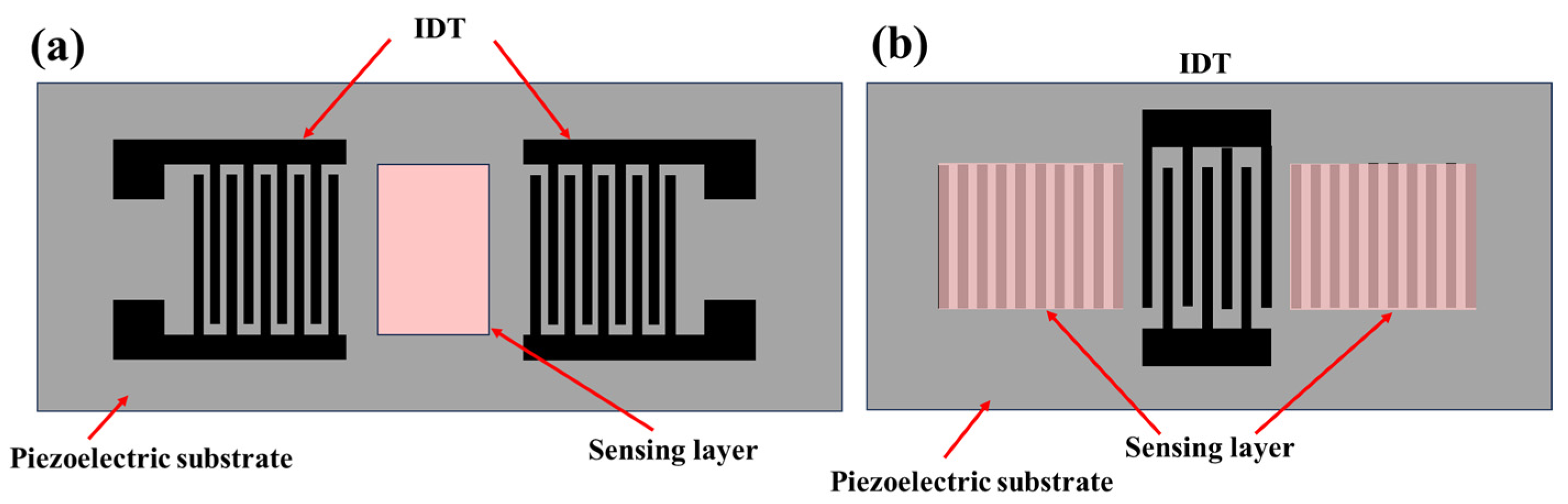
2.1. Mechanisms of SAW Sensors

Surface acoustic waves, initially proposed by Lord Rayleigh in 1885, are a class of mechanical waves that propagate along the surface of an elastic substrate. However, it was not until the 1970s, with the advent of interdigital transducer (IDT) technology and the development of microelectromechanical system (MEMS) techniques, that SAW sensors began to find practical applications in various fields. SAW sensors typically comprise a piezoelectric substrate and interdigital transducers (IDTs), with an optional sensing layer to enhance the interaction with the external environment. The cornerstone of SAW technology is the phenomenon of piezoelectricity, which allows for the conversion of electrical energy into mechanical vibrations and vice versa. The piezoelectricity phenomenon can be observed in anisotropic materials whose internal structures lack a center of symmetry [43]. The most commonly used piezoelectric materials for generating SAWs include quartz, lithium tantalate (LiTaO3), lithium niobate (LiNbO3), and thin films such as AlN, ZnO, and GaN. The major performance parameters of commonly used piezoelectric materials are listed in Table 1 [25,44].
The operating principle of SAW sensors is based on the application of an alternating voltage across IDTs which can induce mechanical displacement on the piezoelectric substrate due to the piezoelectric effect and thereby generate a SAW that travels along the material surface. When external conditions such as temperature, pressure, and humidity change, the propagation characteristics of the SAW (e.g., frequency or acoustic wave velocity) also change accordingly. Therefore, the generated SAWs carry a large amount of environmental information, and the analysis of the SAW’s properties at the receiver end allows for the decoupling and measurement of the physical quantities of interest.
SAW devices are broadly classified into two categories: delay line type and resonator type. Figure 2a illustrates the configuration of a delay line-type SAW device. As shown in Figure 2a, the device consists of a pair of IDTs separated by a distance L on the substrate, where one IDT is responsible for generating the SAW and the other is for reception. This type of SAW devices is widely used in the fields of communication, radar, gas, and biological sensing. Figure 2b illustrates the typical configuration of a resonator type SAW device, which primarily consists of an IDT at the center of the substrate and reflective gratings on both sides, forming a resonant cavity that facilitates coherent reflection and results in a standing wave resonance. This design enables resonator-type SAW devices to have excellent Q factors and reduced insertion loss, making them an ideal choice for high-performance filtering and passive sensors.
During the propagation of SAWs through a piezoelectric medium, there is a coupling between the acoustic wave and the electromagnetic field, implying that the wave’s propagation characteristics can be described by its particle displacement and potential. Therefore, the sensing principle of SAW sensors can be broadly divided into two categories: one involves detecting changes in the strain field, known as mechanical perturbation, which is suitable for detecting physical quantities such as liquid viscosity and mass load; the other involves monitoring changes in the piezoelectric field, known as acoustoelectric interactions, and is suitable for measuring parameters such as liquid conductivity or dielectric constants. For example, SAW UV sensors based on ZnO films primarily operate on the principle of acoustoelectric interactions to detect UV radiation.
The resonant frequency (f) of SAW sensors can typically be described by f = v/λ, where v and λ represent the phase velocity and wavelength, respectively. The phase velocity is sensitive to the perturbation of various physical parameters such as mechanical, electrical, mass, and environmental properties. The impact of changes in external environmental parameters on the phase velocity of SAW can be simply expressed as follows:
d v = V m d m + V E d E + V M i d M i + V e V d e V ,
where m, E, and Mi, ev represent the mass (generally called the mass loading effect, e.g., particles, humidity, gas or biomolecules), electrical properties (e.g., conductivity, often called electrical loading effect), mechanical properties (e.g., elastic modulus or viscosity, sometimes called elastic loading effect), and environmental factors (e.g., temperature), respectively.

2.2. The Wave Modes of SAW Sensors

Under various boundary conditions, different types of SAWs can be excited, including Rayleigh waves, Shear Horizontal (SH) waves, Love waves, and Lamb waves. Each type of SAW mode has different propagation characteristics and is suitable for different application scenarios. Therefore, a comprehensive understanding of the potential SAW modes that can be generated in a piezoelectric substrate is essential and will be discussed in this section.

2.2.1. Rayleigh Waves

The Rayleigh wave is the predominant mode of SAW sensors, with the majority of such sensors being designed to operate on this mode. Rayleigh waves propagate along the surface of a substrate under the condition of semi-infinite boundaries, with their amplitude exponentially decreasing with depth. The penetration depth is typically on the order of one wavelength, which means that the majority of the acoustic energy is concentrated near the substrate’s surface. Rayleigh waves are a combination of both longitudinal and shear vertical vibrations [39]. Thus, surface particles vibrate in an elliptical manner, with their direction being perpendicular to the surface and parallel to the propagation direction [45]. Notably, Rayleigh waves are non-dispersive, with their velocity being solely dependent on the material properties of the substrate and its crystallographic orientation.

2.2.2. Shear Horizontal Waves

In liquid environments, the majority of the acoustic energy of Rayleigh waves is rapidly attenuated due to energy leakage at the solid–liquid interface, which initially limited the application of the SAW technology in liquid-phase sensing. To address this, a SH-SAW sensor is developed to reduce the energy dissipation in liquid phase applications. SH waves are a type of surface waves where particle motion is parallel to the substrate surface but perpendicular to the propagation direction [13]. Therefore, acoustic energy is hardly radiated into the liquid, thus avoiding radiation loss [46]. SH-SAW sensors are not only small and robust but also easy to incorporate into on-line, low-cost systems. Due to these advantages, SH-SAW sensors are widely used for chemical and biochemical detection purposes. The typical operating frequency range for SH-SAW sensors is from 30 MHz to 500 MHz, which is primarily determined by the spacing of the IDTs and phase velocity.

2.2.3. Love Waves

While SH waves are well suited for liquid environments, they are prone to leaking energy into the substrate as the wave propagates over several wavelengths, which diminishes their sensitivity to surface perturbations. To overcome this problem, a layer of low acoustic velocity materials can be deposited on the surface of SH-SAW devices using techniques such as evaporation and sputtering, thereby creating a waveguide layer that allows the wave to decay along the depth of the attached thin layer [47,48,49,50,51]. These types of SH waves are known as Love waves.
Love waves are generated at the interface of two solid elastic substrate layers where one layer is substantially thicker than the other, which is normally a thin overlay. A prerequisite for the excitation of Love waves is that the shear velocity of the overlay material must be less than that of the substrate. Due to the lower shear wave velocity in the waveguide layer, Love waves tend to propagate more within the waveguide layer [52]. By designing an appropriate thickness of the waveguide layer, the energy of SAWs can be effectively concentrated at the surface of the waveguide layer, resulting in greater displacement of surface particles and thus a higher sensitivity to changes in surface mass load. Consequently, Love-mode SAW sensors usually have a higher sensitivity compared to conventional SH-SAW sensors. Moreover, the incorporation of a waveguide layer reduces the leakage of acoustic wave energy and lowers the insertion loss, making it suitable for biosensing or environments with high humidity. Substrates such as different Y-rotated quartz, LiTaO3, and LiNbO3 are suitable for generating Love waves. Waveguide materials such as SiO2, ZnO, PMMA, SU-8 photoresist, and TiO2 are commonly used for guiding layers.

2.2.4. Lamb Waves

Lamb waves are a type of plate waves that are usually generated when the substrate’s thickness is much smaller than or comparable to acoustic wavelengths. The displacement mode of Lamb waves is very similar to that of Rayleigh waves, which are elliptical motions perpendicular and parallel to the surface. Essentially, Lamb waves can be considered as a composite of two sets of Rayleigh waves, each propagating along the corresponding side of a thin plate with a thickness that is less than a single wavelength. In the case of plates with thicknesses that surpass several wavelengths, it can be approximated as the independent propagation of two free Rayleigh waves. According to the propagation modes, Lamb waves can be typically categorized into two types: antisymmetric and symmetric modes. Both modes of waves can propagate through the plate independently depending on the frequency of the wave. Notably, Lamb waves are highly dispersive, with their velocity being influenced by factors such as the properties of the substrate, the thickness of piezoelectric layers, and the intricacies of device design. Generally, Lamb waves have multiple higher-order modes which only emerge when the frequency exceeds the critical frequency. As the plate thickness increases, the critical frequency decreases, leading to a gradual increase in higher-order modes. Therefore, in sensing applications that leverage Lamb waves, lower operating frequencies (typically below 5 MHz) or the use of thinner substrates are often preferred to optimize performances [44,53].
Table 2 provides a summary of the different types of SAWs mentioned above, along with the general materials they are made from, operational frequency ranges, attenuation characteristics, and the advantages they provide [13].

2.3. Performance Indicators of SAW Sensors

To evaluate the performance of a SAW sensor, several critical performance indicators of SAW devices (such as electromechanical coupling coefficient, phase velocity, temperature coefficient of frequency, Q factor) and indicators of sensors (e.g., selectivity, sensitivity, the limit of detection, response time and recovery time) should be considered.
The electromechanical coupling coefficient (k2) is a critical factor for a SAW device, representing the efficiency of converting mechanical energy into electrical energy and vice versa. It can be calculated as the following [13]:
k 2 = e 31 2 c 11 ε 33 ,
where e 31 , c 11 and ε 33 represent the piezoelectric coefficient, the elastic constant, and the dielectric permittivity tensor of a material, respectively. A higher electromechanical coupling coefficient indicates a stronger response of a SAW sensor to external environmental changes, resulting in higher sensitivity. Therefore, selecting piezoelectric materials with a high electromechanical coupling coefficient is crucial for developing high-performance SAW devices.
Phase velocity is another important parameter for a SAW device. Since the resonant frequency of a SAW device is defined as the phase velocity of the wave (v) divided by the periodicity of the IDT (λ), the phase velocity is directly associated with the operating frequency of SAW sensors. Furthermore, phase velocities are influenced by the elastic constants, initial stress, and density of the materials under stress [54,55].
The temperature coefficient of frequency (TCF) is a key indicator reflecting the temperature effect of a SAW device, which can be defined as
T C F = Δ f Δ T × f 0 ,
where Δf represents the change in resonant frequency from the reference temperature to the operating temperature, ΔT is the difference in temperature, and f0 is the resonant frequency at the reference temperature. The TCF reflects the sensitivity of piezoelectric materials to temperature fluctuations. For temperature-sensing applications, a higher TCF means better sensitivity, enabling the detection of smaller temperature fluctuations with a greater resolution. However, for non-temperature sensors, the TCF becomes a factor of interference. Ideally, for such devices, the TCF should approach zero, as any change in the target parameter will inevitably lead to temperature deviations as well.
The Q factor, also known as the quality factor, is a dimensionless parameter that characterizes the energy dissipation or damping in the propagation of acoustic waves on the sensor’s surface. The Q factor is defined as the ratio of the total energy stored in the acoustic wave to the energy dissipated or lost per cycle of oscillation. It can be obtained using the S parameter measurement [56]:
Q = f s / f p 1 f s / f p 2 1 S 12 max S 12 max 1 S 11   min   S 11   min   ,
where S 11 is the reflection signal, S 12 is the transmission signal of the device, and f s and f p represent the series and parallel resonance frequencies, respectively (i.e., polarization is either in phase with the applied electric potential or 180° out of phase with the applied potential, respectively).
Selectivity refers to the degree to which a sensor can distinguish and respond to the analyte (or physical stimulus) of interest in the presence of potential interferents or other substances. It is commonly determined by comparing the signal changes generated by exposure to a certain concentration of the tested analyte to those of an interfering analyte. The selectivity of SAW sensors primarily depends on the material properties of the sensing layer and its interactions with the analyte, including physical adsorption or chemical reactions. Physisorption interactions are reversible and reproducible but generally exhibit lower selectivity. In contrast, devices based on chemisorption demonstrate higher selectivity but usually suffer from poor reversibility and stability.
Sensitivity is a parameter reflecting the ability of a sensor to respond to changes in the concentration of a target analyte (or physical stimulus). It is typically defined as the change in the sensor’s output signal (e.g., frequency shift, phase change, or amplitude variation) per unit change in the analyte’s concentration or mass.
The limit of detection (LoD) is the minimum concentration of a target analyte (or physical stimulus) that a sensor can accurately detect. It is a critical parameter that defines the lowest level at which the sensor can distinguish the analyte signal from the background noise or interference. Both sensitivity and the LoD are key indicators that determine the detection performance of SAW sensors. A sensor with high sensitivity and a low LoD is desirable for accurate and reliable detection and quantification of analytes, especially when dealing with complex matrices or analytes with low concentrations.
The response time of a SAW sensor is defined as the time required for the sensor’s output signal to reach a certain percentage (typically 90%) of its steady-state value after being exposed to the target analyte (or physical stimulus), representing the sensor’s responsiveness.
The recovery time of a SAW sensor is the time required for the sensor’s output signal to return to a certain percentage (typically 90%) of its baseline value after the analyte (or physical stimulus) has been removed. Both response and recovery times are crucial parameters in determining the overall performance and suitability of a SAW sensor for specific applications. For instance, applications that require real-time monitoring or the rapid detection of analytes would necessitate sensors with short response times, while applications involving cyclic or intermittent exposures would benefit from sensors with short recovery times to ensure accurate and reliable measurements.

3. Materials for Sensing Layer of SAW Devices

The sensitive layer is a crucial component of SAW sensors, playing a significant role in achieving a high sensing performance, particularly in gas sensing and biosensing applications. It acts as an intermediary, facilitating the adsorption of the target analyte onto the SAW’s surface. This analyte mass accumulation leads to alterations in the frequency, phase, or wave velocity of SAW devices [57]. Therefore, the sensing layer must possess high sensitivity and selectivity towards the target analyte. Moreover, to ensure that the sensor operates in the best possible parameters, these layers should be thin, uniform, and maintain their chemical and physical stability upon exposure to the test environment. They must also adhere firmly to the substrate without causing any short-circuiting of the IDTs.
In recent years, low-dimensional materials have gained significant attention in sensing applications due to their exceptional properties, such as enhanced sensitivity, substantial electronic bandgaps, rapid response time, and superior selectivity. Based on the morphology and dimensions of these materials, they can be broadly categorized into zero-, one-, and two-dimensional materials [58,59].

3.1. Zero-Dimensional Materials

Zero-dimensional (0-D) materials, such as nanoparticles or quantum dots (QDs), are nanostructures that exhibit confinement in all three spatial dimensions, typically with all dimensions being below 100 nm. Due to their unique quantum confinement effects and high surface-to-volume ratios, 0-D nanomaterials have been widely utilized as sensitive coatings or functionalization layers [60]. These materials are often easily dispersed within a matrix for the fabrication of conductive composites. They have the ability to alter their own conductive properties or modulate the conductive pathways made up of other materials depending on the applied stimulus and sensor structure.
Moreover, 0-D materials possess a large surface area-to-volume ratio, providing numerous active sites for the adsorption of target chemical molecules. This characteristic not only enhances detection sensitivity but also significantly improves response time and reduces the LoD for various gasses and biomolecules. For example, Feng et al. [61] fabricated a SAW near-infrared sensor using MXene QDs as the sensing layer to improve infrared absorption efficiency. The results demonstrated that MXene QDs coating can significantly increase the sensor’s sensitivity from 111.67 to 210.92 kHz/(mW/mm2). Li et al. [62] developed a SAW NO2 sensor based on SnS colloidal quantum dots (CQDs). They successfully synthesized SnS CQDs with average sizes of 5.0 nm and then deposited them onto an ST-cut quartz substrate via the spin-coating method (Figure 3a–c). Due to the efficient adsorption of NO2 gas molecules on the surface of the SnS CQD films, the SAW sensors demonstrated an exceptional ability to detect NO2 at room temperature, showcasing both high sensitivity and selectivity. Similarly, Pasupuleti et al. [63] reported a highly selective NH3 gas sensor based on sulfur-doped graphitic carbon nitride quantum dots (S@g-C3N4 QDs) coated on a langasite (LGS) SAW sensor. The sensor exhibited enhanced sensitivity (∆f=~−27.3 kHz/100 ppm) under UV illumination, with excellent selectivity, good stability, and a low LoD (~85 ppb) for NH3 at room temperature. Additionally, the sensor demonstrated excellent reproducibility and fast response/recovery times under UV activation at 365 nm. The exceptional gas-sensing performance is attributed to the high surface area of the S@g-C3N4 QDs, the presence of enhanced functional groups, sulfur defects, UV-induced photogenerated charge carriers, and efficient charge transfer. These factors collectively enhance the adsorption of gas molecules, leading to an increase in conductivity and, consequently, larger frequency responses.
Due to their nanoscale size, 0-D materials also exhibit efficient dispersibility on the surfaces of other materials. Incorporating a small amount of 0-D materials can result in significant changes in device structures and working mechanisms, leading to remarkable performance enhancements. For example, graphene quantum dots (GQDs), as cost-effective and non-toxic carbon nanomaterials, exhibit exceptional UV absorption and advantageous energy band alignment. These characteristics can effectively enhance the photosensitivity of photoactive materials like ZnO [65]. Yin et al. [64] proposed a flexible SAW sensors using GQD-decorated ZnO nanowires as the sensing layer (Figure 3d,e). Experimental results showed that the UV sensitivity of the sensors increased by three times and the response time decreased by four times (Figure 3f–h). Additionally, the flexible SAW device maintained its performance even under a bending angle of approximately 30° for up to 200 cycles without significant deterioration. Furthermore, incorporating QDs with polymers can enhance their adsorption performance for target chemical substances due to their high specific surface areas [66].

3.2. One-Dimensional Materials

One-dimensional (1-D) nanomaterials, such as nanotubes, nanowires, and nanorods, exhibit anisotropic morphologies and possess high aspect ratios, which provides a unique combination of high surface area and efficient charge transport pathways along their longitudinal axes. These characteristics make 1-D nanomaterials highly suitable for enhancing both the sensitivity and response kinetics of SAW sensors. Additionally, devices constructed from 1-D materials typically exhibit exceptional flexibility and malleability, making them ideal for wearable devices or direct integration into clothing [67].
Nanowires are crystalline nanostructures with diameters that range from a few nanometers to one hundred nanometers and which have demonstrated superior sensing performance compared to thin films [68,69,70]. For example, Marcu et al. [68] deposited ZnO thin films and ZnO nanowires on quartz substrates using laser beam technology, finding that sensors based on ZnO nanowires exhibited higher frequency responses and faster responses to hydrogen and deuterium gas at low concentrations compared to those based on ZnO thin films. ZnO nanowires (888 nm length) also showed higher detection sensitivity (0.062 Hz/ppm) to hydrogen gas compared to ZnO thin films (0.01 Hz/ppm) [70]. Similarly, Peng et al. [69] developed a SAW UV detector based on ZnO nanowires, employing IDTs constructed by the Morlet wavelet function and multiple couplers to enhance the response characteristics of the device. Experimental results indicated that the ZnO nanowire layer exhibited superior UV photoelectric response characteristics compared to sputtered ZnO film layers, with a frequency shift of 65 kHz, approximately eight times higher than the ~8 kHz frequency shift observed with ZnO thin films. Wang et al. [71] proposed using Pd/Cu nanowires with larger surface-to-volume ratio as the sensitive interface to improve the sensitivity and response speed of a SAW H2 gas sensor (Figure 4). This sensor demonstrated excellent repeatability, fast response and recovery times (within 4 s), and a sensitivity of 1.5 kHz/% at room temperature.
Nanorods, another common type of 1-D material, typically exhibit shorter lengths compared to nanowires and have also shown superior properties compared to thin films [72]. Li et al. [72] proposed a room-temperature ammonia sensor based on ST-cut quartz SAW devices, where the sensor coated with ZnO nanorods demonstrated a frequency shift of 1094 Hz to 100 ppm ammonia gas, nearly 3.6 times larger than that of the sensor coated with ZnO nanofilms. Moreover, the SAW sensor coated with ZnO nanorods also showed higher sensitivity when exposed to lower concentrations of ammonia. Guo et al. [73] observed similar results, where a Love-wave-mode SAW humidity sensor coated with ZnO nanorods exhibited improved performance due to their large surface-to-volume ratio.
Carbon nanotubes (CNTs) are another type of 1-D material widely used in the sensing field due to their lightweight nature, high strength, and superior electrical conductivity. In a study by Sayago et al. [74], a composite of polyisobutylene and CNT was used as the sensing layer of a SAW sensor for gas detection. The investigation focused on detecting octane, toluene (volatile organic compounds), and other atmospheric pollutants, including H2, CO, NO2, and NH3, at room temperature. The results showed that even minor proportions of multi-walled CNTs significantly improved the sensor’s response to octane, possibly due to the high surface area, nano dimensions, and hollow structure of CNTs.

3.3. Two-Dimension Materials

Since the groundbreaking isolation of graphene from graphite through micromechanical exfoliation in 2004, two-dimensional (2-D) materials have emerged as a rapidly growing field of research. With numerous pioneering achievements having been reported over the past few decades, significant efforts have been devoted to developing 2-D material-based SAW sensors.
Graphene, a single layer of carbon atoms arranged in a hexagonal lattice, is a type of representative 2-D material that has emerged as a promising material for high-performance sensors due to its remarkable electronic, mechanical, and thermal properties. The high surface area and tunable surface chemistry of graphene enable sensitive detection of a variety of analytes. Additionally, its exceptional electrical conductivity facilitates rapid electron transfers, significantly improving the response time and sensitivity of SAW sensors [75]. For instance, Okuda et al. [76] demonstrated the potential of graphene in the sensing domain by integrating a graphene field-effect transistor with an LiTaO3-based SAW sensor, thus creating a device capable of detecting both charge and mass with high sensitivity. Preparing high-quality graphene in large quantities; however, remains challenging. Compared with graphene, both graphene oxide (GO) and reduced graphene oxide (rGO) can be considered as being defective forms of graphene. These 2-D materials can be synthesized through facile and low-cost solution methods and can be easily dispersed in matrixes, which provides great convenience for building composite sensing layers. Similarly to graphene, GO and rGO are also excellent sensing materials due to their abundant active sites [77]. Li et al. [78] fabricated a SAW H2 sensor based on a composite of GO and palladium nanoparticles (PdNPs). The GO/PdNP-based SAW sensor exhibited a sensitivity of 2070 Hz/1000 ppm in the hydrogen concentration range of 0–3000 ppm. Furthermore, the sensor demonstrated good stability and a fast response time (6 s) and recovery time (7 s). Lim et al. [79] fabricated a LGS SAW NO2 gas sensor using a p-phenylenediamine-rGO (PrGO) nanocomposite as a sensing layer. They found that PrGO significantly increased the resonant frequency change in the sensor (~3.5 kHz) when exposed to 100 ppm NO2 gas, which is almost eight times higher than that of a bare LGS sensor. The enhanced sensitivity of the PrGO-coated LGS sensor can be attributed to the abundance of amine functional groups in p-phenylenediamine and the hydroxyl (OH) chemical groups on the surface of the rGO nanosheets.
Transition metal chalcogenide-based materials are another class of 2-D materials, consisting of transition metal atoms bonded to chalcogen atoms in a layered structure [31,32]. The layered structure and various transition metal/chalcogen combinations endow these materials with diverse properties and potential applications for electronics, optoelectronics, and sensing. Additionally, with their characteristic of having a direct bandgap, transition metal chalcogenides are expected to overcome the limitation of graphene being used as a semiconductor due to their zero bandgap and demonstrate excellent semiconductor performance. Zhou et al. [80] reported a SAW UV sensor using 2-D wide bandgap semiconductor MoS2 nanosheets as a UV photo-conductive material (Figure 5). The sensor demonstrated high sensitivity to UV radiation (2.05 ppm/μW·cm−2), with a maximum frequency shift reaching 3.5 MHz under 365 nm UV irradiation. The high sensitivity is attributed to the high resonant frequency (~1.02 GHz) and the high specific surface area of MoS2 nanosheets. Lu et al. [81] developed a high-performance SAW humidity sensor using SnO2 /MoS2 nanocomposites as a sensing layer. The sensor demonstrated good linearity with a correlation coefficient (R2) exceeding 0.98 across the entire detection range of 10–90% RH. It also exhibited high sensitivity (0.78 kHz/%RH and 8.87 ppm/%RH), low hysteresis characteristics, good repeatability, and long-term stability.
MXenes are a type of transition metal carbides, nitrides, or carbonitrides with a two-dimensional layered structure. They were first synthesized and named by Dr. Yury Gogotsi and his colleagues in 2011 [82]. Due to thier excellent electrical conductivity, rich surface functional groups, strong hydrophilicity, and good chemical stability, MXenes have garnered widespread attention in gas-sensing applications. Li et al. [83] developed a SAW NO2 gas sensor with composites of MXene and GO nanosheets deposited on its surface. The MXene/GO SAW sensor exhibited a higher frequency shift (−1.58 kHz) compared to the GO SAW sensor (∼−0.14 kHz) when exposed to 10 ppm NO2 gas (Figure 6a–c). This enhanced sensitivity can be credited to the large number of active functional groups (such as -OH, -O, and -COOH), abundant active surface sites, and high charge transfer rate of the MXene/GO composite material. Moreover, the MXene/GO SAW sensor demonstrated good stability and reproducibility, faster response and recovery times, and excellent durability under different relative humidity conditions (Figure 6d–f). Similarly, Pasupuleti et al. [84] reported a SAW sensor based on ZnO@Ti3C2Tx MXene hybrid composites for ultrahigh NH3 gas detection (Figure 6g,h). Under UV illumination, the sensor demonstrated exceptional sensing performance in regard to NH3, with an enhanced frequency response (~32.24 kHz/20 ppm), good selectivity, low detection limit (~89.41 ppb), long-term stability, and robust sensitivity.

4. Coating Techniques for Low-Dimensional Materials

Coating techniques play a crucial role in the integration of low-dimensional materials into SAW sensors. The selection of coating technique significantly influences the material’s properties, uniformity, and overall performance in various applications. This section aims to provide a short overview of commonly used deposition techniques employed for low-dimensional materials, followed by a comparative analysis of these methods, as shown in Table 3.

4.1. Spin Coating

Spin coating is a widely used technique for depositing thin films onto flat substrates by rotating the substrate at high speed. The principle of spin coating relies on the centrifugal force generated during the rotation, which causes the coating solution to spread outwards from the center of the substrate. As the substrate spins, the coating solution thins out into a uniform film due to the centrifugal force and solvent evaporation. The final film thickness is determined by several factors, including the viscosity of the coating solution, the percentage of the solid in the solution, the surface tension, volatility of the solvent, spin speed, and spin time. Generally, higher spin speeds and lower viscosities result in thinner films.
Owing to its high reproducibility, cost efficiency, and ability to operate at room temperature, spin coating is suitable for the deposition of a variety of low-dimensional materials, such as quantum dots, carbon nanotubes, GO, and rGO. For example, Li et al. [62] utilized spin coating to form a high-quality SnS colloidal quantum dot (CQD) sensing layer on a piezoelectric substrate by spinning at 2000 rpm for 45 s. However, this technique is primarily applicable to flat substrates and suffers from the problem of material wastage. Typically, only 2–5% of the material applied to the substrate is effectively utilized during the spin-coating process, with the remaining 95–98% being wasted and dispersed within the dispensing vessel. Moreover, this technique is primarily used for thin film deposition on small-sized substrates and is not suitable for large-area film fabrication.

4.2. Inkjet Printing

Inkjet printing is a non-contact, pressure-free deposition technique that forms desired patterns by ejecting ink droplets onto a substrate. With the advantages of accuracy, high resolution, and high speed [85], inkjet printing is an ideal tool for precisely positioning the coatings onto SAW devices. Furthermore, compared to spin coating, inkjet printing has high material utilization efficiency and is suitable for both flat and curved substrates. This method is capable of depositing a wide range of liquids, such as polymers, ZnO nanowires, and graphene-based materials, onto a variety of substrates at room temperature. For example, Nikolaou et al. [86] reported a Love-wave SAW sensor using inkjet-printed GO as sensing layers, which demonstrated excellent sensitivities to C2H6O, C7H8, and water molecules. However, this method has high requirements regarding the properties of the ink solution, especially in terms of viscosity and surface tension. Additionally, the uniformity and reproducibility of this method are not enough when it comes to the fabrication of large-area films.

4.3. Chemical Vapor Deposition

Chemical vapor deposition (CVD) stands out as one of the most promising techniques for the industrial-scale synthesis of 2-D material films, such as graphene-based materials, Mxene, and transition metal chalcogenide-based materials. The fundamental principle of CVD involves the introduction of gaseous reactants, such as methane, ethane, or propane, onto a substrate, typically copper or nickel. This process enables the nucleation and growth of 2-D material films, such as graphene, on the substrate during the cooling phase. CVD is capable of producing high-quality films with excellent uniformity and adherence. By carefully adjusting parameters such as temperatures, deposition durations, pressures, gas compositions, and flow rates, the thickness of the films can be precisely controlled to meet the requirements of various applications. However, it is important to note that film quality, structure, and growth kinetics are significantly influenced by temperature, which can reach levels of between 600 and 1000 degrees Celsius, thereby posing challenges in certain scenarios.
To prevent thermal damage to piezoelectric substrates and IDTs, a two-step process can be employed wherein low-dimensional materials are initially grown on a metal substrate via CVD before being transferred to SAW devices. For instance, in study [75], monolayer graphene films were first synthesized on Cu foils through CVD. Subsequently, spin coating was utilized to apply a protective layer of polymethyl methacrylate (PMMA) onto the graphene surface. After dissolving the metal substrate in an etching solution, the graphene/PMMA layer was transferred to the surface of a SAW device. The PMMA was subsequently removed using acetone, yielding a high-quality monolayer graphene sensing layer.

4.4. Pulsed Laser Deposition

Pulsed Laser Deposition (PLD) is a widely used physical vapor deposition technique. Briefly, its main principle is to use high-energy laser pulses to ablate the target material, generating a plume of atoms and molecules that are then deposited onto the substrate to form a thin film. Possessing the advantages of a high deposition rate, the ability to preserve the stoichiometry of the target, and relatively high reproducibility [87,88], PLD is well suited to the growth of low-dimensional materials with various morphologies and properties. Furthermore, the film thickness can be precisely controlled by adjusting parameters such as laser power, pulse frequency, deposition pressure, and deposition rate, enabling the fabrication of films with atomic-level precision. Consequently, PLD has been extensively utilized for the deposition of sensitive layers in SAW sensors, such as the Pd/ZnO bilayer [89], Pd/TiO2 bilayer [90], and ZnO nanowires [68,70]. However, PLD usually requires high vacuum conditions and sophisticated equipment, which can add complexity and cost to the deposition process. Additionally, the deposition area is often limited, rendering it unsuitable for large-scale manufacturing applications

5. Applications of SAW Sensors Based on Low-Dimensional Materials
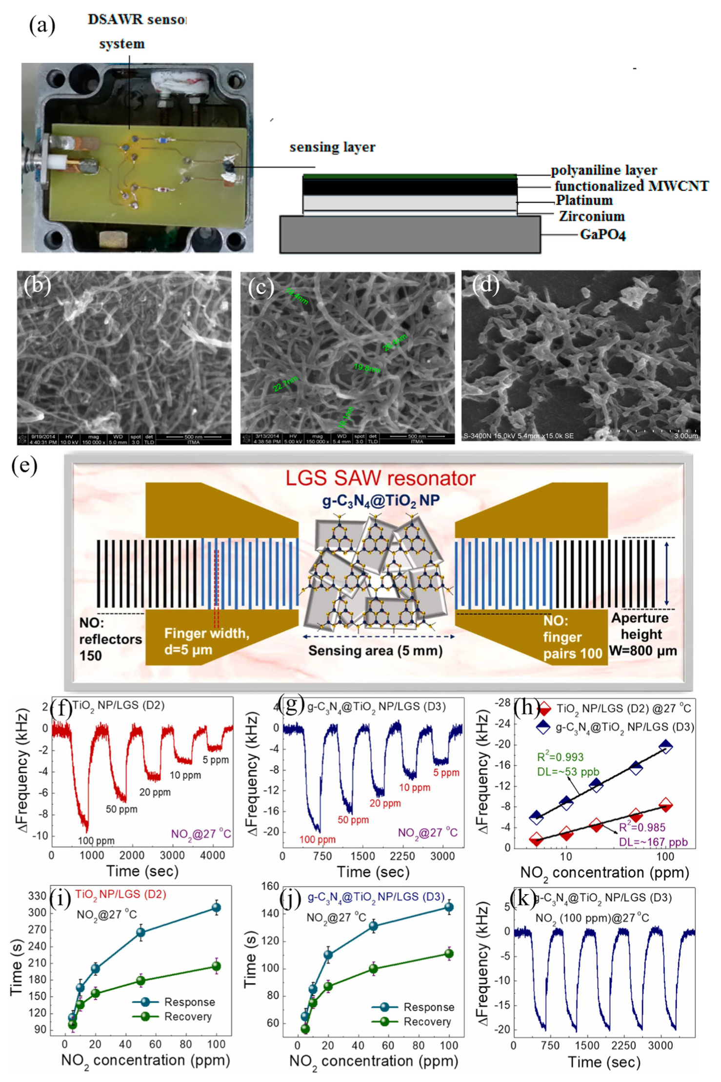
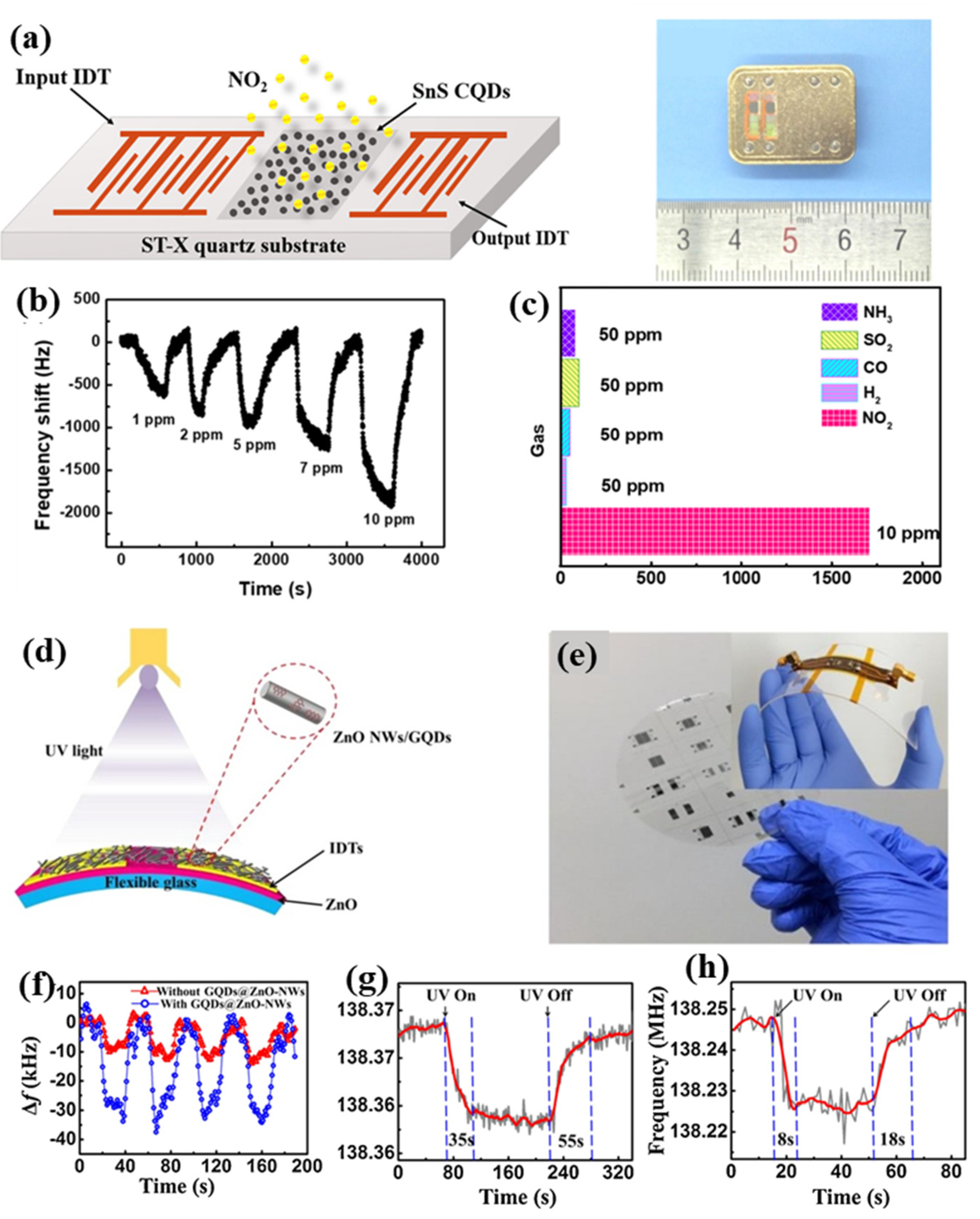
5.1. Gas Sensors

Over the past several decades, SAW technology has been widely applied in chemical and gas sensing due to its strong anti-interference capability, low cost, high sensitivity, and passive and wireless capability [91]. The SAW gas sensor detects the concentration of a specific gas in the environment through the propagation of surface acoustic waves on a piezoelectric substrate. A sensing layer with high sensitivity and selectivity for the target gas is typically coated on the piezoelectric substrate, which adsorbs the target gas molecules in the air and causes a mass loading effect. Accordingly, the phase velocity and resonant frequency will change. Xu et al. [92] fabricated a SAW sensor containing a graphene/nickel/L-alanine composite sensing film for CO2 gas detection. The sensor demonstrated high sensitivity, with a frequency response to CO2 concentrations of 2.51 MHz ppm−1 m−2 within the range of 0 to 2000 ppm and 0.46 MHz ppm−1 m−2 from 2000 to 38,500 ppm. The integration of graphene and nickel nanoparticles within the composite layer significantly amplified the sensor’s sensitivity, attributed to their facilitation of gas adsorption and catalytic reactions. Wang et al. [93] proposed a novel passive wireless SAW CO2 sensor based on a CNT thin film (Figure 7). The sensor benefits from the expansive surface area of the CNT-PEI nanocomposite, achieving a minimal detection threshold of 1% CO2 concentration with a frequency alteration of 0.0036%.
SAW devices are often used to detect toxic, harmful, flammable, or explosive gasses, such as nitrogen oxides (NO and NO2), hydrogen (H2), ammonia (NH3), and H2S [41,83,94,95]. For example, Huang et al. [96] proposed a SAW sensor coated with a poly(4-styrenesulfonic acid)-doped PPy/WO3/rGO hybrid nanocomposite sensing film. This sensor exhibited exceptional sensitivity to NO gas (12 Hz/ppb) over a detection range of 1 to 110 ppb. It also demonstrated fast response and recovery times, with an LoD that reaches 0.31 ppb for a signal-to-noise ratio of 3.
NH3 is another toxic gas that is often emitted as a byproduct of chemical combustion processes in various industrial processes. Excessive amounts of NH3 pose a significant threat to both animals and plants [97]. To monitor the concentration of NH3, Yang et al. [98] developed a novel room-temperature NH3 gas sensor based on a Pd/SnO2/rGO ternary nanocomposite film. The strategic incorporation of Pd and rGO nanoparticles into the composite material remarkedly amplified the sensor’s affinity for NH3, particularly at low concentrations. Consequently, the sensor manifested high sensitivity even at a low concentration of NH3 (5 ppm), coupled with commendable linearity over the range of 5 to 150 ppm. Sun et al. [99] demonstrated a novel SAW sensor coated with GO-SnO2 nanocomposites for NH3 detection. The sensor exhibited exceptional performance, achieving an ultra-low detection limit of 40 ppb with fast response times of less than 16.4 s at room temperature.
H2 is also a widely used industrial gas that is very dangerous due to its explosive nature [100]. For H2 detection, Yunusa et al. [101] developed a dual SAW resonator system, employing a sensing layer comprising functionalized multi-walled carbon nanotubes (MWCNTs) and polyaniline nanofibers (Figure 8a–d). The introduction of OOH groups by the MWCNTs endowed the sensor with high sensitivity (3.2 Hz/ppm) for H2 gas concentrations ranging from 1% to 2%. However, the instability of the polyaniline nanofibers compromised the sensor’s applicability. Kim et al. [102] presented a highly sensitive and selective SAW H2 sensor. A beehive-configured and Cu-doped SnO2 nanostructure was utilized as the sensitive material, providing a high surface-to-volume ratio, high sensitivity, and selectivity for hydrogen detection. With the capability to discern a minimum frequency difference of approximately 1 Hz, the sensor achieved the detection of H2 concentrations below 1 ppm coupled with commendable selectivity (0.063 kHz ppm−1), repeatability, and long-term stability. Wang et al. [71] improved the response speed and sensitivity of a SAW hydrogen gas sensor by employing palladium and copper nanowires and achieved a low detection limitation of 7 ppm and a fast response and recovery within 4s. Jin et al. [103] used a two-dimensional Zeolitic imidazole framework as anti-interference layers on PdNi films to improve the H2 sensing performance, achieving an ultralow limit of detection of 5 ppm and outstanding selectivity for H2 gas against other gasses (CO/NH3/H2S). The improved H2 sensing performance has been attributed to the fact that the two-dimensional anti-interference layer (2-D ZIF) is more conducive to the diffusion of gas molecules, which in turn increases the interaction between PdNi and the target gas.
Volatile organic compounds (VOCs) have emerged as a critical public health concern due to their ubiquitous presence in a variety of commercial products and industrial applications [104]. These compounds are associated with a plethora of health issues, including cardiovascular disease, cancer, and neurological damage [105]. To achieve low-cost VOC detection, Nikolaou et al. [106] fabricated a Love-mode SAW sensor, leveraging inkjet-printed GO as a sensing layer. Due to the substantial adsorptive capacity of GO for vaporous compounds, the sensor demonstrated a sensitivity of 30 Hz/ppm and 24 Hz/ppm for C2H6O and C7H8, respectively.
The mass-loading mechanism is one of the principal methods for gas detection using SAW devices. However, this method encounters limitations when the incremental mass due to gas concentration is minimal, resulting in negligible frequency shifts. Metal oxide-based composite nanofilms can improve the sensitivity, as these also utilize the conduction changes within the sensing layers themselves [107,108,109,110,111]. Raj et al. [112] synthesized four types of metal oxides (ZnO, TeO2, SnO2, and TiO2) with uniform thickness (40 nm) via radio-frequency sputtering and evaluated their ammonia adsorption efficacy. The ZnO film emerged as the most sensitive to ammonia, attributed to its high intrinsic defect density, including zinc vacancies, oxygen vacancies, and anti-site defects, which collectively bolster the film’s ammonia adsorption capacity [113]. Wang et al. [19] developed a SAW H2S gas sensor based on CuO/SnO2 composite films fabricated by radio-frequency magnetron sputtering. The sensor demonstrated a sensitivity of 16.9 kHz/ppm along with excellent selectivity and repeatability. The incorporation of metallic dopants, such as Pd, into metal oxide-based nanomaterials can further improve the performance of the sensing layer [90,114]. Huang et al. [115] presented a SAW hydrogen gas sensor using Pt-coated ZnO nanorods as the sensing layer, demonstrating frequency shifts of 8.36 kHz and 26 kHz in response to hydrogen concentrations of 200 ppm and 6000 ppm, respectively. This performance surpasses that of SAW devices based on pure ZnO nanorods or ZnO thin films. Moreover, the sensor achieves a nearly 90% steady state in less than 15 s, with a recovery time of approximately 2–3 min. The enhanced response was credited to Pt doping, which not only augments the adsorptive properties of ZnO for gas molecules but also functions as a catalyst to accelerate surface reaction kinetics, thus enhancing the sensor’s response rate and sensitivity. Additionally, the integration of CNT into metal oxide nanomaterials can also significantly enhance the gas detection performance of SAW sensors [116].
However, slow response and recovery times remain a challenge in SAW-based gas sensing. To solve this problem, Li et al. [117] leveraged solution-processed PbS colloidal QDs as the sensing layer of SAW devices for the detection of NO2 at room temperature. The sensor displayed an elevated frequency shift of 9.8 kHz with a relatively fast response time (45 s) and recovery time (58 s) upon exposure to 10 ppm of NO2 gas. Similarly, Wen et al. [118] fabricated a novel NO2 gas sensor using a dual track SAW device, demonstrating good reproducibility, fast response, and excellent stability across NO2 concentrations from 0.5 to 10 ppm. Pasupuleti et al. [119] integrated 2-D g-C3N4 with TiO2 NPs as the sensing layer of a SAW device for NO2 gas detection, as shown in Figure 8e. The frequency shift (∆f) of the sensor is about 19.8 kHz toward 100 ppm of NO2 at room temperature (Figure 8g), which is 2.4 times higher than that of the pristine TiO2 NP/LGS SAW sensor (Figure 8f). The sensor also demonstrated an enhanced sensitivity, LoD, response/recovery kinetics, and stability relative to common interfering gasses such as NO, CO, H2S, and NH3 (Figure 8h–k). This superior performance stems from the large surface area, oxygen vacancies, and OH/amine functional groups within the g-C3N4@TiO2 nanoparticle heterojunction microstructure, providing abundant active sites for the adsorption and diffusion of NO2 molecules.
Figure 8. (a) Fabricated sensor with the MWNT sensing layer integrated into the system placed in a test cell; (bd) SEM micrograph of MWNT, functionalized CNT, and polyaniline nanofibers, respectively. Reproduced with permission from [101] (Copyright 2015, MDPI). (e) Schematic of the LGS SAW sensor deposited with g-C3N4@TiO2 NP hybrid nanocomposite over the sensing area. (f) Schematic illustration of the fabricated LGS SAW resonating sensor deposited with the g-C3N4@TiO2 NP hybrid nanocomposite. (f,g) Time-dependent frequency transient NO2 gas responses of pristine TiO2 NP/LGS and g-C3N4@TiO2 NP/LGS SAW sensors at RT. (h) The frequency responses, (i,j) response and recovery times, and (k) cycling stability of g-C3N4@TiO2 NP/LGS SAW sensor. Reproduced with permission from [119] (Copyright 2022, Elsevier).
Chemosensors 12 00255 g008

5.2. UV Sensors

UV radiation, a form of electromagnetic radiation with wavelengths ranging from 10 to 450 nm, has a significant impact on both environmental and human health. Consequently, the development of UV photodetectors is of paramount importance. These devices can be affixed to the skin to monitor UV radiation intensity from sunlight, thereby protecting against skin diseases [120]. Among various UV sensors, SAW-based UV detectors stand out due to their unique advantages, including remote and wireless operation capabilities and the potential for zero-power consumption. Typically, the surface of a SAW device is coated with a layer of photoactive material serving as a sensing layer for UV detection. Upon exposure to UV radiation, the photogenerated carriers excite acoustic and electrical effects, resulting in changes to the resonant frequency, phase, and amplitude of the SAW device.
The choice of sensitive materials is crucial for the performance of SAW UV sensors, as these directly influence sensitivity, response/recovery times, and repeatability [25]. ZnO is a widely used photoactive material, and its micro and nano structures are broadly applied in SAW UV detectors. Wang et al. [121] reported a high-precision UV detector that integrates ZnO nanostructures with a dual delay line SAW oscillator system. The maximum frequency shift in the detector can reach 40 kHz under 365 nm illumination across several on–off cycles, surpassing AlGaN-based SAW UV detectors by a factor of six. Guo et al. [122] fabricated a high-sensitivity SAW UV detector using ZnO nanowires as the sensing layer. They systematically investigated the contributions of acoustoelectric and thermal effects at varying UV radiation intensities and discovered that the acoustoelectric effect dominates at low UV intensities (<30 mW/cm2) while the thermal effect becomes predominant at higher intensities (>90 mW/cm2) due to the saturation of photogenerated carriers in ZnO nanowires.
Doping ZnO nanostructures with elements such as gold (Au), silver (Ag), aluminum (Al), tin (Sn), and copper (Cu) has been shown to significantly enhance the performance of UV detectors. For example, Fu et al. [123] developed a SAW UV detector based on Ag-doped ZnO nanoparticles. Ag doping effectively increases the conductivity of the ZnO films, thereby improving the sensitivity of SAW sensors. Specifically, the device achieved a sensitivity of 0.2 dB/(μW·cm–2) under UV irradiation at a wavelength of 365 nm.
Owing to their robust chemical and mechanical stability, superior photoelectric performance, and the versatility of nanostructures, TiO2 thin films with varied surface morphologies and nanostructures have been widely investigated to boost light absorption in photodetector applications [124,125,126]. Walter et al. [127] proposed a SAW UV detector, employing a TiO2 thin film with nanorods as the sensing layer. The TiO2 thin film was deposited on 128° Y−cut LiNbO3 substrate through the radio-frequency magnetron sputtering, followed by the hydrothermal synthesis of TiO2 nanorods on the deposited film. The device exhibited a pronounced increase in phase shift under 365 nm UV illumination, rising from 5.96° for the bare TiO2 thin film to 77.42° with the introduction of nanorods. This enhancement is predominantly ascribed to the superior photoelectric activity of the TiO2 nanostructure and its augmented UV light absorption efficiency.

5.3. Humidity Sensors
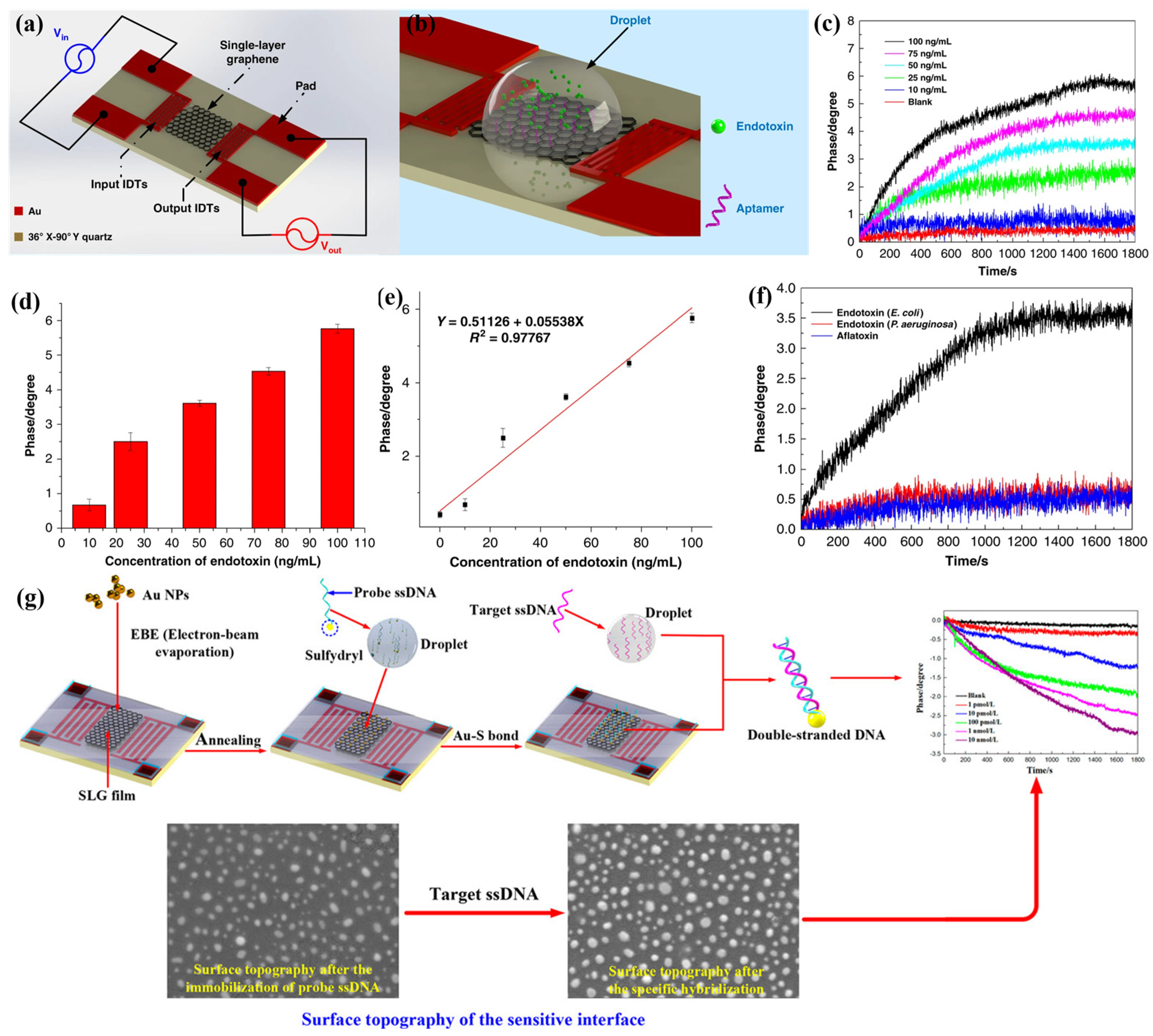
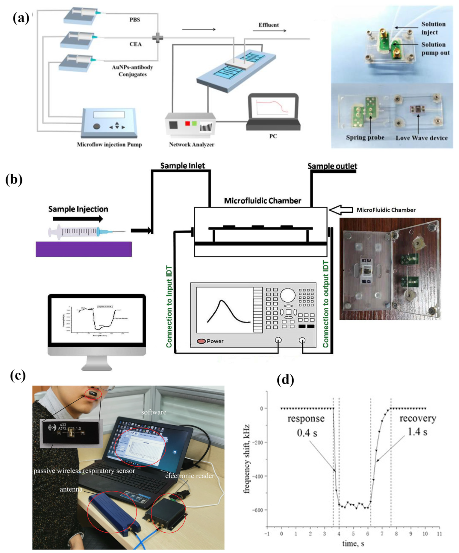
Humidity is a crucial environmental parameter that significantly affects air quality, human comfort, agricultural productivity, and the efficacy of various industrial processes. The precise monitoring and regulation of humidity levels are thus imperative for optimizing conditions across a spectrum of applications, including agriculture, manufacturing, and health monitoring. The principle of SAW humidity sensors is similar to that of SAW gas sensors. It is primarily based on the resonance frequency shifts caused by the adsorption of water molecules on the sensing layer, involving both mass loading and electric loading effects.
To date, materials used in SAW humidity sensors predominantly encompass thin films and nanostructures of ZnO, such as nanowires, nanorods, and nanobelts, as well as two-dimensional materials like graphene, metal oxides, and their composites [25]. ZnO, being hydrophilic and sensitive to humidity, has been widely used in humidity sensors. For instance, He et al. [128] fabricated high-sensitivity SAW humidity sensors based on nanocrystalline ZnO/polyimide substrates, achieving a sensitivity of 34.7 kHz/10% RH without any surface treatment. However, metal-oxide-film-based SAW devices often encounter problems such as long response times and substantial hysteresis [128]. To solve these issues, Wu et al. [129] developed a transparent and ultrasensitive flexible SAW humidity sensor (see Figure 9), employing a composite sensing layer of ZnO nanowires and GQDs. The integration of ZnO nanowires increases the specific surface area, providing more active sites for water molecule adsorption during humidity sensing [130]. Additionally, GQDs can enhance the water adsorbing capacity of ZnO [131]. Consequently, the sensitivity was greatly increased, reaching 40.16 kHz/% RH, along with its excellent stability and repeatability.
Graphene and its derivatives have also been widely used in SAW humidity sensors. For example, Su et al. [132] developed a flexible SAW humidity sensor based on a three-dimensional architecture of a graphene (3DAG)/polyvinyl alcohol (PVA)/SiO2 layered sensing film, as illustrated in Figure 10a. This sensor exhibited a humidity resolution of 0.25% in the relative humidity range of 5% to 55% and a resolution of 0.10% in the range of 55% to 90%, primarily due to the synergistic effects of the viscoelastic properties of the PVA film, the large adsorption and transport capacity of the 3DAG, and the mass loading effect of the SiO2 (Figure 10b). Furthermore, this humidity sensor was employed for breath monitoring, showcasing its capability in detecting varying breathing rates and depths as well as human dehydration. Le et al. [133] applied a uniform and highly oxidized GO film on a SAW humidity sensor, achieving a sensitivity of 25.3 kHz/% RH across a wide range from 10% RH to 90% RH with minimal hysteresis. Xuan et al. [134] developed a flexible ZnO/PI SAW humidity sensor using GO as the sensing layer, demonstrating a significantly enhanced sensitivity compared to sensors without the GO layer. This enhancement has been attributed to the hydrophilic nature of the GO film, which improves water adsorption due to its oxygen-rich groups, thereby amplifying the mass loading effect and inducing a larger frequency shift. Additionally, the GO films substantially increase the effective sensing area, thereby drastically improving sensitivity. Le et al. [135] also observed that employing a GO sensing layer can substantially enhance the sensitivity of the SAW humidity sensor at a high level of relative humidity levels (above 80%).
Furthermore, low-dimensional polymer compounds can also be used as the sensing layer of SAW humidity sensors. Liu et al. [136] developed a high-frequency SAW humidity sensor based on CeO2 nanoparticles/polyvinyl pyrrolidone nanofibers. The increased electrical conductivity of CeO2/PVP nanofibers at high RH led to an additional acoustoelectric loading effect, thereby enhancing the frequency response. Moreover, the inorganic/organic nanohybrid-based SAW sensor exhibited high stability in humid environments and demonstrated negligible cross-sensitivity effects, enabling reliable wireless humidity detection.
Despite the significant enhancement in sensitivity offered by the incorporation of low-dimensional nanomaterials in SAW humidity sensors, challenges persist. For instance, the reproducibility of nanofilm fabrication remains insufficient, and the performance of the sensing layer can fluctuate during the device’s deformation process if applied in flexible and wearable fields.

5.4. Biosensors

Over the past few decades, great efforts have been devoted to developing novel biosensing technologies for disease diagnosis. Among numerous biosensors, SAW sensors have distinguished themselves as a promising option due to their accuracy, compact size, and wireless access capability. In general, SAW devices function as biosensors by binding target biomolecules to recognition molecules immobilized on the surface of sensing materials, which results in a change in the mass and induces a shift in resonant frequency. By monitoring these changes in resonant frequency, both qualitative and quantitative analyses of the target biomolecules can be performed with high sensitivity and accuracy.
With the increasing utilization of nanomaterials, particularly two-dimensional materials, in SAW sensors, their sensitivity and selectivity have been significantly enhanced. Given the predominance of liquid environments in biological detection, SH and Love wave modes are the most commonly used modes in SAW biosensors. Li et al. [137] developed a highly sensitive Love-mode SAW immunosensor for detecting carcinoembryonic antigens (CEAs), as shown in Figure 11a. The innovative use of gold nanoparticles bound to CEA antibodies significantly amplified the mass loading effect, enhancing the sensor’s maximum responses by an impressive 30-fold. The immunosensor’s resonant frequency correlates linearly with CEA concentrations ranging from 0.2 to 5 ng/mL, with the LoD reaching as low as 0.2 ng/mL. Additionally, it exhibited minimal interference from nonspecific adsorption, making it a potential candidate for point-of-care detection of cancer markers. In a similar study, Jandas et al. [138] synthesized a novel polymer nanocomposite thin film incorporating polyimide, rGO, MoS2, and anionic nanoparticles. This composite film served as the transducing bioreceptor base of a SAW biosensor for the selective detection of CEA (Figure 11b). The integration of conducting polymers and rGO effectively reduces the high insertion loss typically associated with polymer-based SAWs, thereby enhancing sensitivity. The biosensor exhibited a frequency shift (Δf) of around 150 Hz in response to a 0.1 ng/mL of CEA solution, with an LoD of approximately 0.084 ng/mL. Remarkably, it displayed exceptional selectivity for CEA, with negligible cross-reactivity with common tumor-marker proteins such as AFP, CA 125, and l-tryptophan.
Monitoring respiratory characteristics is essential for diagnosing sleep respiratory disorders such as obstructive sleep apnea syndrome. Feng et al. [139] proposed a passive wireless respiratory sensor based on a flexible SAW device that utilizes GO as a sensing layer. As illustrated in Figure 11c, the sensor was placed on the upper lip below the nose to detect humidity changes during inhalation and exhalation, thus monitoring sleep-disordered breathing by recording human breathing patterns. The sensor also demonstrated a fast response time (0.4 s) and a fast recovery time (1.4 s), as shown in Figure 11d, with a capability to measure over 33 breaths per minute, exceeding the average number of breaths per minute in adults (16–20 breaths per minute).
SAW devices have shown outstanding performance in the detection of cells and viral pathogens [140,141,142]. Among the materials for biomolecule immobilization, graphene-based nanomaterials stand out due to their exceptional biocompatibility and sensing properties [143,144,145,146,147]. Ji et al. [75] reported a label-free and highly sensitive SH SAW biosensor using a single-layer graphene (SLG) film for endotoxin detection (Figure 12a,b). The SLG film was deposited on a quartz substrate. Acrylic materials and cross-linking aptamers with glutaraldehyde (a substance with high affinity and specificity to bind to a target molecule) were immobilized to enhance hydrophilicity and biorecognition capabilities. This biosensor exhibited a linear detection sensitivity for endotoxins in the concentration range of 0 to 100 ng/mL, achieving an LoD of 3.53 ng/mL (Figure 12c–f). In addition, it displayed excellent stability and specificity, although its repeatability still needed further improvement.
Furthermore, SAW technology has also been applied to the detection of gene sequences [148] and proteins [149]. Ji et al. [150] developed an SLG/Au NPs-based Love-wave SAW biosensor for the detection of Staphylococcus aureus gene sequences (Figure 12g). A chemical vapor deposition-grown SLG film with a thickness of 0.3–0.4 nm was deposited onto the surface of the sensitive area. To further amplify the signal of the biosensor, Au NPs were subsequently deposited on the SLG film via electron-beam evaporation [151,152,153], resulting in a uniform dispersion across the surface. The biosensors exhibited excellent sensitivity, with an LoD of 1.86 pmol/L (12.4 pg/mL). Furthermore, the biosensors demonstrated excellent stability in liquid media, with a deviation lower than 0.1° over a duration of 0.5 h, indicating their potential for reliable and sensitive detection of target analytes. In protein detection, CNTs provide an effective platform for both nonspecific protein adsorption and specific protein binding [154,155,156]. Wu et al. [157] fabricated a novel CNT-coated parylene-C film and employed it as the acoustic-waveguiding layer for a cell-based Love-wave SAW biosensor. This modified sensor can be used for label-free detection of proteins released during platelet activation. Results showed that the CNT-enhanced SAW sensor demonstrated a higher resonance frequency shift, sensitivity, and consistency compared to sensors with only parylene-C film.
However, the selectivity of SAW biosensors for specific targets in environments with multiple interfering elements still needs improvement. Moreover, flexible, wearable, wireless, self-powered, and adaptive will be the development directions of SAW biosensors in the future.
Figure 12. (a,b) A schematic of the SH-SAW biosensor chip and the working principles. (c) The real-time monitoring phase shift signals of the specific binding of the aptamer and the endotoxin at different concentrations. (d) A histogram of the specific binding of the aptamer to the endotoxin at different concentrations. (e) A standard curve for the quantitative detection of an endotoxin with an SH-SAW biosensor based on SLG. (f) The real-time phase signals of the endotoxin obtained from E. coli, the endotoxin obtained from P. aeruginosa, and the aflatoxin binding with the aptamer, which were all analyzed at concentrations of 50 ng/mL. Reproduced with permission from [75] (Copyright 2020, Springer Nature). (g) Schematic diagram of a single-layered graphene/Au-nanoparticle-based Love-wave biosensor. Reproduced with permission from [150] (Copyright 2020, American Chemical Society).
Chemosensors 12 00255 g012

6. Conclusions and Future Perspectives

6.1. Conclusions

This review provides a comprehensive summary of recent advancements in SAW sensors based on low-dimensional materials. It discusses the fundamental mechanisms of SAW sensors along with key parameters influencing the sensing performance. A wide range of low-dimensional materials, including 0-D, 1-D, and 2-D materials, utilized as efficient sensing materials in SAW sensors are reviewed. The review demonstrates that the application of these nanomaterials as sensing layers can dramatically improve detection capabilities, resulting in more rapid, selective, and accurate sensing. Key applications of SAW devices coated with low-dimensional materials in different fields, such as gas detection, UV sensing, humidity monitoring, and biosensing, are summarized. Furthermore, the challenges and prospects of employing low-dimensional materials to further enhance SAW sensors are also discussed.

6.2. Future Perspectives

In recent years, incorporating low-dimensional materials into the sensing layer of SAW sensors has emerged as a promising strategy to enhance their sensing capabilities. These nanomaterials, either embedded within the active region or used as a coating, offer a large surface area and abundant surface functional groups, making them ideal for the adsorption of target analytes. However, the practical application of low-dimensional materials in SAW sensors still faces several challenges. For example, some functional groups of low-dimensional materials strongly rely on the oxidation process, which results in a reduction in pore size and surface area, consequently leading to longer response and recovery times [158,159]. The presence of multiple oxygen-containing functional groups in materials, such as MXenes and graphene-based materials, may lead to their decomposition at high operating temperatures, causing a decline in sensitivity [160]. Additionally, during the gas adsorption process, physical adsorption often occurs alongside chemical adsorption. This chemical interaction between gas molecules and the surface functional groups of the sensing layer can lead to incomplete recovery and the poor repeatability of sensors [160,161]. Doping with other active catalyst materials like conductive polymers, organic materials and metal nanoparticles are proved to be an effective way to address these problems [158].
Furthermore, the scalability of low-dimensional materials from the laboratory level to the industry level remains a formidable challenge. Existing synthesis methods are often tailored for small-scale production, and scaling up to large-scale manufacturing while maintaining cost-effectiveness is crucial for the broad adoption of these materials in SAW sensors. Ensuring reproducible synthesis and achieving batch-to-batch consistency with uniform material properties is also of paramount importance. However, achieving this consistency can be challenging, as the synthesis processes often require intricate techniques and precise control over reaction conditions. Another concern is the susceptibility of low-dimensional materials to environmental factors such as humidity and temperature, making it essential to ensure their stability and robustness under diverse operating conditions for reliable sensor performances.
With the booming development of flexible electronics, flexible and wearable sensors have become an important development goal for SAW devices in the future [25]. Consequently, the compatibility between low-dimensional materials and flexible piezoelectric substrates is an issue that needs to be addressed, requiring robust adhesion while minimizing propagation losses [162]. The inherent mismatch in mechanical properties and thermal expansion coefficients between these materials and their substrates can cause delamination or degradation under bending or flexing conditions. This is especially critical for materials like graphene and CNTs, which may have superior mechanical properties but require rigorous evaluation of their performance and stability under repeated stress. Furthermore, many applications of flexible SAW sensors require devices that are not only stretchable but also conformable. This necessitates SAW sensors based on low-dimensional materials being insensitive to strain, as the frequency shift in flexible SAW sensors can be markedly influenced by strain and mechanical deformation. A promising strategy to address this challenge is to devise a methodology for extracting pivotal information from the scattering parameters of flexible SAW devices. By integrating machine learning or artificial intelligence techniques, it is possible to decouple the influences of multiple parameters and achieve anti-strain interference effects [163].

Author Contributions

Conceptualization, Q.L.; data curation, Q.L., C.Z.; writing—original draft preparation, Q.L.; writing—review and editing, Q.L. and H.X.; visualization, Q.L., C.Z. and M.L.; funding acquisition, Q.L. and H.X. All authors have read and agreed to the published version of the manuscript.

Funding

The work was supported by the Natural Science Foundation of Sichuan Province under Grant No. 2022NSFSC0516, the National Natural Science Foundation of China under Grant No. 62004025, and the Scientific Research Foundation for Yangtze Delta Region Institute (Huzhou) of University of Electronic Science and Technology of China under Grant No. U03220153.

Institutional Review Board Statement

Not applicable.

Informed Consent Statement

Not applicable.

Data Availability Statement

Not applicable.

Conflicts of Interest

The authors declare no conflicts of interest.

References

  1. Xu, K.; Lu, Y.; Takei, K. Multifunctional Skin-Inspired Flexible Sensor Systems for Wearable Electronics. Adv. Mater. Technol. 2019, 4, 1800628. [Google Scholar] [CrossRef]
  2. Zhang, K.; Wang, Y.; Yang, Y. Structure Design and Performance of Hybridized Nanogenerators. Adv. Funct. Mater. 2019, 29, 1806435. [Google Scholar] [CrossRef]
  3. Hua, Q.; Sun, J.; Liu, H.; Bao, R.; Yu, R.; Zhai, J.; Pan, C.; Wang, Z.L. Skin-Inspired Highly Stretchable and Conformable Matrix Networks for Multifunctional Sensing. Nat. Commun. 2018, 9, 244. [Google Scholar] [CrossRef] [PubMed]
  4. Wu, J.; Wu, Z.; Ding, H.; Wei, Y.; Yang, X.; Li, Z.; Yang, B.-R.; Liu, C.; Qiu, L.; Wang, X. Multifunctional and High-Sensitive Sensor Capable of Detecting Humidity, Temperature, and Flow Stimuli Using an Integrated Microheater. ACS Appl. Mater. Interfaces 2019, 11, 43383–43392. [Google Scholar] [CrossRef] [PubMed]
  5. Länge, K. Bulk and Surface Acoustic Wave Sensor Arrays for Multi-Analyte Detection: A Review. Sensors 2019, 19, 5382. [Google Scholar] [CrossRef] [PubMed]
  6. Cruz, C.; Matatagui, D.; Ramírez, C.; Badillo-Ramirez, I.; de la O-Cuevas, E.; Saniger, J.M.; Horrillo, M.C. Carbon SH-SAW-Based Electronic Nose to Discriminate and Classify Sub-Ppm NO2. Sensors 2022, 22, 1261. [Google Scholar] [CrossRef] [PubMed]
  7. Agostini, M.; Cecchini, M. Ultra-High-Frequency (UHF) Surface-Acoustic-Wave (SAW) Microfluidics and Biosensors. Nanotechnology 2021, 32, 312001. [Google Scholar] [CrossRef]
  8. Schmid, L.; Weitz, D.A.; Franke, T. Sorting Drops and Cells with Acoustics: Acoustic Microfluidic Fluorescence-Activated Cell Sorter. Lab Chip 2014, 14, 3710–3718. [Google Scholar] [CrossRef]
  9. Hassan, M.M.; Sium, F.S.; Islam, F.; Choudhury, S.M. A Review on Plasmonic and Metamaterial Based Biosensing Platforms for Virus Detection. Sens. Bio-Sens. Res. 2021, 33, 100429. [Google Scholar] [CrossRef]
  10. Jiang, Y.; Tan, C.Y.; Tan, S.Y.; Wong, M.S.F.; Chen, Y.F.; Zhang, L.; Yao, K.; Gan, S.K.E.; Verma, C.; Tan, Y.-J. SAW Sensor for Influenza A Virus Detection Enabled with Efficient Surface Functionalization. Sens. Actuat. B-Chem. 2015, 209, 78–84. [Google Scholar] [CrossRef]
  11. Zhang, J.; Zhang, X.; Wei, X.; Xue, Y.; Wan, H.; Wang, P. Recent Advances in Acoustic Wave Biosensors for the Detection of Disease-Related Biomarkers: A Review. Anal. Chim. Acta 2021, 1164, 338321. [Google Scholar] [CrossRef]
  12. Gray, E.R.; Turbé, V.; Lawson, V.E.; Page, R.H.; Cook, Z.C.; Ferns, R.B.; Nastouli, E.; Pillay, D.; Yatsuda, H.; Athey, D.; et al. Ultra-Rapid, Sensitive and Specific Digital Diagnosis of HIV with a Dual-Channel SAW Biosensor in a Pilot Clinical Study. NPJ Digital Med. 2018, 1, 35. [Google Scholar] [CrossRef]
  13. Mandal, D.; Banerjee, S. Surface Acoustic Wave (SAW) Sensors: Physics, Materials, and Applications. Sensors 2022, 22, 820. [Google Scholar] [CrossRef] [PubMed]
  14. Damasceno, B.S.; Horta, I.M.; de Oliveira, R.S.; Pereira, R.M.; Schatkoski, V.M.; Bacher, G.; Leite, D.M. Recent Improvements on Surface Acoustic Wave Sensors Based on Graphenic Nanomaterials. Mat. Sci. Semicon. Proc. 2023, 167, 107811. [Google Scholar] [CrossRef]
  15. Li, D.; Feng, Y.; Zhou, L.; Ye, Z.; Wang, J.; Ying, Y.; Ruan, C.; Wang, R.; Li, Y. Label-Free Capacitive Immunosensor Based on Quartz Crystal Au Electrode for Rapid and Sensitive Detection of Escherichia Coli O157:H7. Anal. Chim. Acta 2011, 687, 89–96. [Google Scholar] [CrossRef]
  16. Liu, X.; Wang, J.-Y.; Mao, X.-B.; Ning, Y.; Zhang, G.-J. Single-Shot Analytical Assay Based on Graphene-Oxide-Modified Surface Acoustic Wave Biosensor for Detection of Single-Nucleotide Polymorphisms. Anal. Chem. 2015, 87, 9352–9359. [Google Scholar] [CrossRef] [PubMed]
  17. Branch, D.W.; Hayes, D.C.; Ricken, J.B. Handheld Biosensor for COVID-19 Screening. Sandia National Laboratory Report No. SAND-2020-10358. September 2020. Available online: https://www.osti.gov/biblio/1671376/ (accessed on 1 September 2020).
  18. Chivukula, V.S.; Ciplys, D.; Kim, J.H.; Rimeika, R.; Xu, J.M.; Shur, M.S. Surface Acoustic Wave Response to Optical Absorption by Graphene Composite Film. IEEE T Ultrason. Ferr. 2012, 59, 265–270. [Google Scholar] [CrossRef] [PubMed]
  19. Guo, Y.J.; Zhao, C.; Zhou, X.S.; Li, Y.; Zu, X.T.; Gibson, D.; Fu, Y.Q. Ultraviolet Sensing Based on Nanostructured ZnO/Si Surface Acoustic Wave Devices. Smart Mater. Struct. 2015, 24, 125015. [Google Scholar] [CrossRef]
  20. Li, C.; Kan, H.; Luo, J.; Fu, C.; Zhou, J.; Liu, X.; Wang, W.; Wei, Q.; Fu, Y. A High Performance Surface Acoustic Wave Visible Light Sensor Using Novel Materials: Bi2S3 Nanobelts. RSC Adv. 2020, 10, 8936–8940. [Google Scholar] [CrossRef]
  21. Oh, H.; Lee, K.J.; Baek, J.; Yang, S.S.; Lee, K. Development of a High Sensitive pH Sensor Based on Shear Horizontal Surface Acoustic Wave with ZnO Nanoparticles. Microelectron. Eng. 2013, 111, 154–159. [Google Scholar] [CrossRef]
  22. Wang, T.; Green, R.; Guldiken, R.; Mohapatra, S.; Mohapatra, S. Multiple-Layer Guided Surface Acoustic Wave (SAW)-Based pH Sensing in Longitudinal FiSS-Tumoroid Cultures. Biosens. Bioelectron. 2019, 124–125, 244–252. [Google Scholar] [CrossRef] [PubMed]
  23. Jin, P.; Fu, J.; Wang, F.; Zhang, Y.; Wang, P.; Liu, X.; Jiao, Y.; Li, H.; Chen, Y.; Ma, Y.; et al. A Flexible, Stretchable System for Simultaneous Acoustic Energy Transfer and Communication. Sci. Adv. 2021, 7, eabg2507. [Google Scholar] [CrossRef] [PubMed]
  24. Kim, Y.; Suh, J.M.; Shin, J.; Liu, Y.; Yeon, H.; Qiao, K.; Kum, H.S.; Kim, C.; Lee, H.E.; Choi, C.; et al. Chip-Less Wireless Electronic Skins by Remote Epitaxial Freestanding Compound Semiconductors. Science 2022, 377, 859–864. [Google Scholar] [CrossRef] [PubMed]
  25. Zhou, J.; Guo, Y.; Wang, Y.; Ji, Z.; Zhang, Q.; Zhuo, F.; Luo, J.; Tao, R.; Xie, J.; Reboud, J.; et al. Flexible and Wearable Acoustic Wave Technologies. Appl. Phys. Rev. 2023, 10, 021311. [Google Scholar] [CrossRef]
  26. Chen, Y.; Shu, Z.; Zhang, S.; Zeng, P.; Liang, H.; Zheng, M.; Duan, H. Sub-10 Nm Fabrication: Methods and Applications. Int. J. Extrem. Manuf. 2021, 3, 032002. [Google Scholar] [CrossRef]
  27. Zhang, Y.; Tan, Y.-W.; Stormer, H.L.; Kim, P. Experimental Observation of the Quantum Hall Effect and Berry’s Phase in Graphene. Nature 2005, 438, 201–204. [Google Scholar] [CrossRef]
  28. Stoller, M.D.; Park, S.; Zhu, Y.; An, J.; Ruoff, R.S. Graphene-Based Ultracapacitors. Nano Lett. 2008, 8, 3498–3502. [Google Scholar] [CrossRef]
  29. Buckley, D.J.; Black, N.C.G.; Castanon, E.G.; Melios, C.; Hardman, M.; Kazakova, O. Frontiers of Graphene and 2D Material-Based Gas Sensors for Environmental Monitoring. 2D Mater. 2020, 7, 032002. [Google Scholar] [CrossRef]
  30. Chhowalla, M.; Shin, H.S.; Eda, G.; Li, L.-J.; Loh, K.P.; Zhang, H. The Chemistry of Two-Dimensional Layered Transition Metal Dichalcogenide Nanosheets. Nat. Chem. 2013, 5, 263–275. [Google Scholar] [CrossRef] [PubMed]
  31. Huang, X.; Zeng, Z.; Zhang, H. Metal Dichalcogenide Nanosheets: Preparation, Properties and Applications. Chem. Soc. Rev. 2013, 42, 1934–1946. [Google Scholar] [CrossRef]
  32. Chhowalla, M.; Liu, Z.; Zhang, H. Two-Dimensional Transition Metal Dichalcogenide (TMD) Nanosheets. Chem. Soc. Rev. 2015, 44, 2584–2586. [Google Scholar] [CrossRef] [PubMed]
  33. Osada, M.; Sasaki, T. Exfoliated Oxide Nanosheets: New Solution to Nanoelectronics. J. Mater. Chem. 2009, 19, 2503–2511. [Google Scholar] [CrossRef]
  34. Pawar, K.K.; Kumar, A.; Mirzaei, A.; Kumar, M.; Kim, H.W.; Kim, S.S. 2D Nanomaterials for Realization of Flexible and Wearable Gas Sensors: A Review. Chemosphere 2024, 352, 141234. [Google Scholar] [CrossRef]
  35. Bhati, V.S.; Kumar, M.; Banerjee, R. Gas Sensing Performance of 2D Nanomaterials/Metal Oxide Nanocomposites: A Review. J. Mater. Chem. C 2021, 9, 8776–8808. [Google Scholar] [CrossRef]
  36. Zhang, H. Ultrathin Two-Dimensional Nanomaterials. ACS Nano 2015, 9, 9451–9469. [Google Scholar] [CrossRef] [PubMed]
  37. Lee, C.; Wei, X.; Kysar, J.W.; Hone, J. Measurement of the Elastic Properties and Intrinsic Strength of Monolayer Graphene. Science 2008, 321, 385–388. [Google Scholar] [CrossRef]
  38. Varghese, S.S.; Varghese, S.H.; Swaminathan, S.; Singh, K.K.; Mittal, V. Two-Dimensional Materials for Sensing: Graphene and Beyond. Electronics 2015, 4, 651–687. [Google Scholar] [CrossRef]
  39. Lamanna, L. Recent Progress in Polymeric Flexible Surface Acoustic Wave Devices: Materials, Processing, and Applications. Adv. Mater. Technol. 2023, 8, 2300362. [Google Scholar] [CrossRef]
  40. Yin, H.; Cao, Y.; Marelli, B.; Zeng, X.; Mason, A.J.; Cao, C. Soil Sensors and Plant Wearables for Smart and Precision Agriculture. Adv. Mater. 2021, 33, 2007764. [Google Scholar] [CrossRef]
  41. Kumar, A.; Prajesh, R. The Potential of Acoustic Wave Devices for Gas Sensing Applications. Sens. Actuat. A-Phys. 2022, 339, 113498. [Google Scholar] [CrossRef]
  42. Weser, R.; Winkler, A.; Weihnacht, M.; Menzel, S.; Schmidt, H. The Complexity of Surface Acoustic Wave Fields Used for Microfluidic Applications. Ultrasonics 2020, 106, 106160. [Google Scholar] [CrossRef] [PubMed]
  43. Qu, S.; Sheng, P. Microwave and Acoustic Absorption Metamaterials. Phys. Rev. Appl. 2022, 17, 047001. [Google Scholar] [CrossRef]
  44. Fu, Y.Q.; Luo, J.K.; Nguyen, N.T.; Walton, A.J.; Flewitt, A.J.; Zu, X.T.; Li, Y.; McHale, G.; Matthews, A.; Iborra, E.; et al. Advances in Piezoelectric Thin Films for Acoustic Biosensors, Acoustofluidics and Lab-on-Chip Applications. Prog. Mater. Sci. 2017, 89, 31–91. [Google Scholar] [CrossRef]
  45. Oh, H.; Lee, K.; Eun, K.; Choa, S.-H.; Yang, S.S. Development of a High-Sensitivity Strain Measurement System Based on a SH SAW Sensor. J. Micromech. Microeng. 2012, 22, 025002. [Google Scholar] [CrossRef]
  46. Kondoh, J.; Matsui, Y.; Shiokawa, S.; Wlodarski, W.B. Enzyme-Immobilized SH-SAW Biosensor. Sens. Actuat. B-Chem. 1994, 20, 199–203. [Google Scholar] [CrossRef]
  47. Newton, M.I.; McHale, G.; Martin, F. Experimental Study of Love Wave Devices with Thick Guiding Layers. Sens. Actuat. A-Phys. 2004, 109, 180–185. [Google Scholar] [CrossRef]
  48. Zhang, F.; Li, S.; Cao, K.; Wang, P.; Su, Y.; Zhu, X.; Wan, Y. A Microfluidic Love-Wave Biosensing Device for PSA Detection Based on an Aptamer Beacon Probe. Sensors 2015, 15, 13839–13850. [Google Scholar] [CrossRef] [PubMed]
  49. Lee, S.; Kim, K.-B.; Kim, Y.-I. Love Wave SAW Biosensors for Detection of Antigen-Antibody Binding and Comparison with SPR Biosensor. Food Sci. Biotechnol. 2011, 20, 1413–1418. [Google Scholar] [CrossRef]
  50. Roach, P.; Atherton, S.; Doy, N.; McHale, G.; Newton, M.I. SU-8 Guiding Layer for Love Wave Devices. Sensors 2007, 7, 2539–2547. [Google Scholar] [CrossRef]
  51. McHale, G.; Newton, M.I.; Martin, F.; Gizeli, E.; Melzak, K.A. Resonant Conditions for Love Wave Guiding Layer Thickness. Appl. Phys. Lett. 2001, 79, 3542–3543. [Google Scholar] [CrossRef]
  52. Trivedi, S.; Nemade, H.B. Finite Element Simulation of Love Wave Resonator for DNA Detection. Int. J. Adv. Eng. Sci. Appl. Math. 2015, 7, 210–218. [Google Scholar] [CrossRef]
  53. Lamb, H. On Waves in an Elastic Plate. Proc. R. Soc. Lond. Ser. A 1917, 93, 114–128. [Google Scholar]
  54. Zhou, J.; Ji, Z.; Guo, Y.; Liu, Y.; Zhuo, F.; Zheng, Y.; Gu, Y.; Fu, Y.; Duan, H. Strategy to Minimize Bending Strain Interference for Flexible Acoustic Wave Sensing Platform. NPJ Flex. Electron. 2022, 6, 84. [Google Scholar] [CrossRef]
  55. Ahmed, I.; Rawat, U.; Chen, J.-T.; Weinstein, D. Super-High-Frequency Low-Loss Sezawa Mode SAW Devices in a GaN/SiC Platform. IEEE Trans. Ultrason. Ferr. 2023, 70, 291–301. [Google Scholar] [CrossRef] [PubMed]
  56. Hara, M.; Kuypers, J.; Abe, T.; Esashi, M. Surface Micromachined AlN Thin Film 2 GHz Resonator for CMOS Integration. Sens. Actuat. A-Phys. 2005, 117, 211–216. [Google Scholar] [CrossRef]
  57. Hamidon, M.N.; Yunusa, Z.; Hamidon, M.N.; Yunusa, Z. Sensing Materials for Surface Acoustic Wave Chemical Sensors. In Progresses in Chemical Sensor; IntechOpen: London, UK, 2016; pp. 161–179. [Google Scholar]
  58. Hung, C.M.; Van Duy, N.; Van Quang, V.; Van Toan, N.; Van Hieu, N.; Hoa, N.D. Facile Synthesis of Ultrafine rGO/WO3 Nanowire Nanocomposites for Highly Sensitive Toxic NH3 Gas Sensors. Mater. Res. Bull. 2020, 125, 110810. [Google Scholar] [CrossRef]
  59. Vargas-Bernal, R. Electrical Properties of Two-Dimensional Materials Used in Gas Sensors. Sensors 2019, 19, 1295. [Google Scholar] [CrossRef]
  60. Gogola, J.L.; Martins, G.; Gevaerd, A.; Blanes, L.; Cardoso, J.; Marchini, F.K.; Banks, C.E.; Bergamini, M.F.; Marcolino-Junior, L.H. Label-Free Aptasensor for P24-HIV Protein Detection Based on Graphene Quantum Dots as an Electrochemical Signal Amplifier. Anal. Chim. Acta 2021, 1166, 338548. [Google Scholar] [CrossRef]
  61. Feng, L.; Liu, G.; Guo, P.; Jiang, Y.; Ma, X.; Chen, Y.; Luo, J. High-Sensitivity Non-Cooled near-Infrared Detector Based on Lithium Niobate Surface Acoustic Wave Resonators Combined with MXene Ti3C2Tx Quantum Dot Thin Films. Opt. Express 2023, 31, 25829–25839. [Google Scholar] [CrossRef]
  62. Li, H.; Li, M.; Kan, H.; Li, C.; Quan, A.; Fu, C.; Luo, J.; Liu, X.; Wang, W.; Yang, Z.; et al. Surface Acoustic Wave NO2 Sensors Utilizing Colloidal SnS Quantum Dot Thin Films. Surf. Coat. Tech. 2019, 362, 78–83. [Google Scholar] [CrossRef]
  63. Pasupuleti, K.S.; Chougule, S.S.; Vidyasagar, D.; Bak, N.; Jung, N.; Kim, Y.-H.; Lee, J.-H.; Kim, S.-G.; Kim, M.-D. UV Light Driven High-Performance Room Temperature Surface Acoustic Wave NH3 Gas Sensor Using Sulfur-Doped g-C3N4 Quantum Dots. Nano Res. 2023, 16, 7682–7695. [Google Scholar] [CrossRef]
  64. Yin, C.; Wu, J.; Zhou, J.; Zhang, D.; Liu, Z.; Liu, X.; Liu, L.; Zhan, Z.; Garner, S.; Fu, Y. Enhancing the Sensitivity of Flexible Acoustic Wave Ultraviolet Photodetector with Graphene-Quantum-Dots Decorated ZnO Nanowires. Sens. Actuators A Phys. 2021, 321, 112590. [Google Scholar] [CrossRef]
  65. Dhar, S.; Majumder, T.; Mondal, S.P. Graphene Quantum Dot-Sensitized ZnO Nanorod/Polymer Schottky Junction UV Detector with Superior External Quantum Efficiency, Detectivity, and Responsivity. ACS Appl. Mater. Interfaces 2016, 8, 31822–31831. [Google Scholar] [CrossRef]
  66. Constantinoiu, I.; Viespe, C. Hydrogen Detection with SAW Polymer/Quantum Dots Sensitive Films. Sensors 2019, 19, 4481. [Google Scholar] [CrossRef] [PubMed]
  67. Xu, Q.; Dai, Y.; Peng, Y.; Hong, L.; Yang, N.; Wang, Z. Recent Development of Multifunctional Sensors Based on Low-Dimensional Materials. Sensors 2021, 21, 7727. [Google Scholar] [CrossRef] [PubMed]
  68. Marcu, A.; Viespe, C. Surface Acoustic Wave Sensors for Hydrogen and Deuterium Detection. Sensors 2017, 17, 1417. [Google Scholar] [CrossRef] [PubMed]
  69. Peng, W.; He, Y.; Wen, C.; Ma, K. Surface Acoustic Wave Ultraviolet Detector Based on Zinc Oxide Nanowire Sensing Layer. Sens. Actuat. A-Phys. 2012, 184, 34–40. [Google Scholar] [CrossRef]
  70. Marcu, A.; Viespe, C. Laser-Grown ZnO Nanowires for Room-Temperature SAW-Sensor Applications. Sensors Actuat. B-Chem. 2015, 208, 1–6. [Google Scholar] [CrossRef]
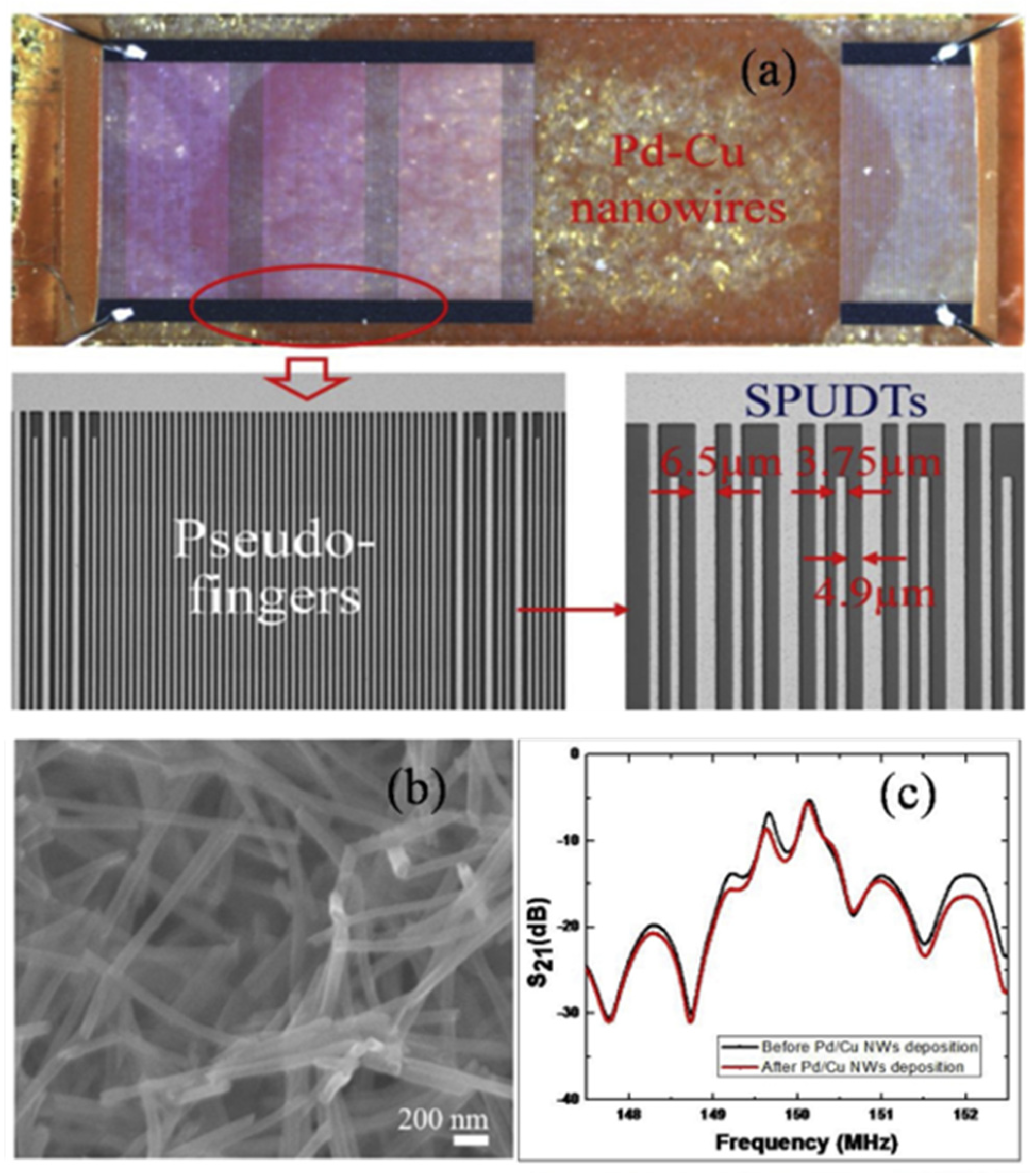
  71. Wang, W.; Liu, X.; Mei, S.; Jia, Y.; Liu, M.; Xue, X.; Yang, D. Development of a Pd/Cu Nanowires Coated SAW Hydrogen Gas Sensor with Fast Response and Recovery. Sensors Actuat. B-Chem. 2019, 287, 157–164. [Google Scholar] [CrossRef]
  72. Li, W.; Guo, Y.; Tang, Y.; Zu, X.; Ma, J.; Wang, L.; Fu, Y.Q. Room-Temperature Ammonia Sensor Based on ZnO Nanorods Deposited on ST-Cut Quartz Surface Acoustic Wave Devices. Sensors 2017, 17, 1142. [Google Scholar] [CrossRef]
  73. Guo, Y.J.; Zhang, J.; Zhao, C.; Ma, J.Y.; Pang, H.F.; Hu, P.A.; Placido, F.; Gibson, D.; Zu, X.T.; Zu, H.Y.; et al. Characterization and Humidity Sensing of ZnO/42° YX LiTaO3 Love Wave Devices with ZnO Nanorods. Mater. Res. Bull. 2013, 48, 5058–5063. [Google Scholar] [CrossRef]
  74. Sayago, I.; Fernández, M.J.; Fontecha, J.L.; Horrillo, M.C.; Vera, C.; Obieta, I.; Bustero, I. Surface Acoustic Wave Gas Sensors Based on Polyisobutylene and Carbon Nanotube Composites. Sensors Actuat. B-Chem. 2011, 156, 1–5. [Google Scholar] [CrossRef]
  75. Ji, J.; Pang, Y.; Li, D.; Huang, Z.; Zhang, Z.; Xue, N.; Xu, Y.; Mu, X. An Aptamer-Based Shear Horizontal Surface Acoustic Wave Biosensor with a CVD-Grown Single-Layered Graphene Film for High-Sensitivity Detection of a Label-Free Endotoxin. Microsyst. Nanoeng. 2020, 6, 4. [Google Scholar] [CrossRef]
  76. Okuda, S.; Ono, T.; Kanai, Y.; Ikuta, T.; Shimatani, M.; Ogawa, S.; Maehashi, K.; Inoue, K.; Matsumoto, K. Graphene Surface Acoustic Wave Sensor for Simultaneous Detection of Charge and Mass. ACS Sens. 2018, 3, 200–204. [Google Scholar] [CrossRef] [PubMed]
  77. Dinu, L.A.; Buiculescu, V.; Baracu, A.M. Recent Progress on Nanomaterials for NO2 Surface Acoustic Wave Sensors. Nanomaterials 2022, 12, 2120. [Google Scholar] [CrossRef] [PubMed]
  78. Li, D.; Le, X.; Pang, J.; Xie, J. A Saw Hydrogen Sensor Based on the Composite of Graphene Oxide and Palladium Nanoparticles. In Proceedings of the 2019 IEEE 32nd International Conference on Micro Electro Mechanical Systems (MEMS), Seoul, Republic of Korea, 27–31 January 2019. [Google Scholar]
  79. Lim, J.-B.; Reddeppa, M.; Nam, D.; Pasupuleti, K.S.; Bak, N.-H.; Kim, S.-G.; Cho, H.D.; Kim, M.-D. Surface Acoustic Device for High Response NO2 Gas Sensor Using P-Phenylenediamine-Reduced Graphene Oxide Nanocomposite Coated on Langasite. Smart Mater. Struct. 2021, 30, 095016. [Google Scholar] [CrossRef]
  80. Zhou, P.; Chen, C.; Wang, X.; Hu, B.; San, H. 2-Dimentional Photoconductive MoS2 Nanosheets Using in Surface Acoustic Wave Resonators for Ultraviolet Light Sensing. Sens. Actuat. A-Phys. 2018, 271, 389–397. [Google Scholar] [CrossRef]
  81. Lu, L.; Liu, J.; Li, Q.; Yi, Z.; Liu, J.; Wang, X.; Chen, X.; Yang, B. High Performance SnO2/MoS2-Based Surface Acoustic Wave Humidity Sensor With Good Linearity. IEEE Sens. J. 2019, 19, 11027–11033. [Google Scholar] [CrossRef]
  82. Naguib, M.; Kurtoglu, M.; Presser, V.; Lu, J.; Niu, J.; Heon, M.; Hultman, L.; Gogotsi, Y.; Barsoum, M.W. Two-Dimensional Nanocrystals Produced by Exfoliation of Ti3AlC2. Adv. Mater. 2011, 23, 4248–4253. [Google Scholar] [CrossRef]
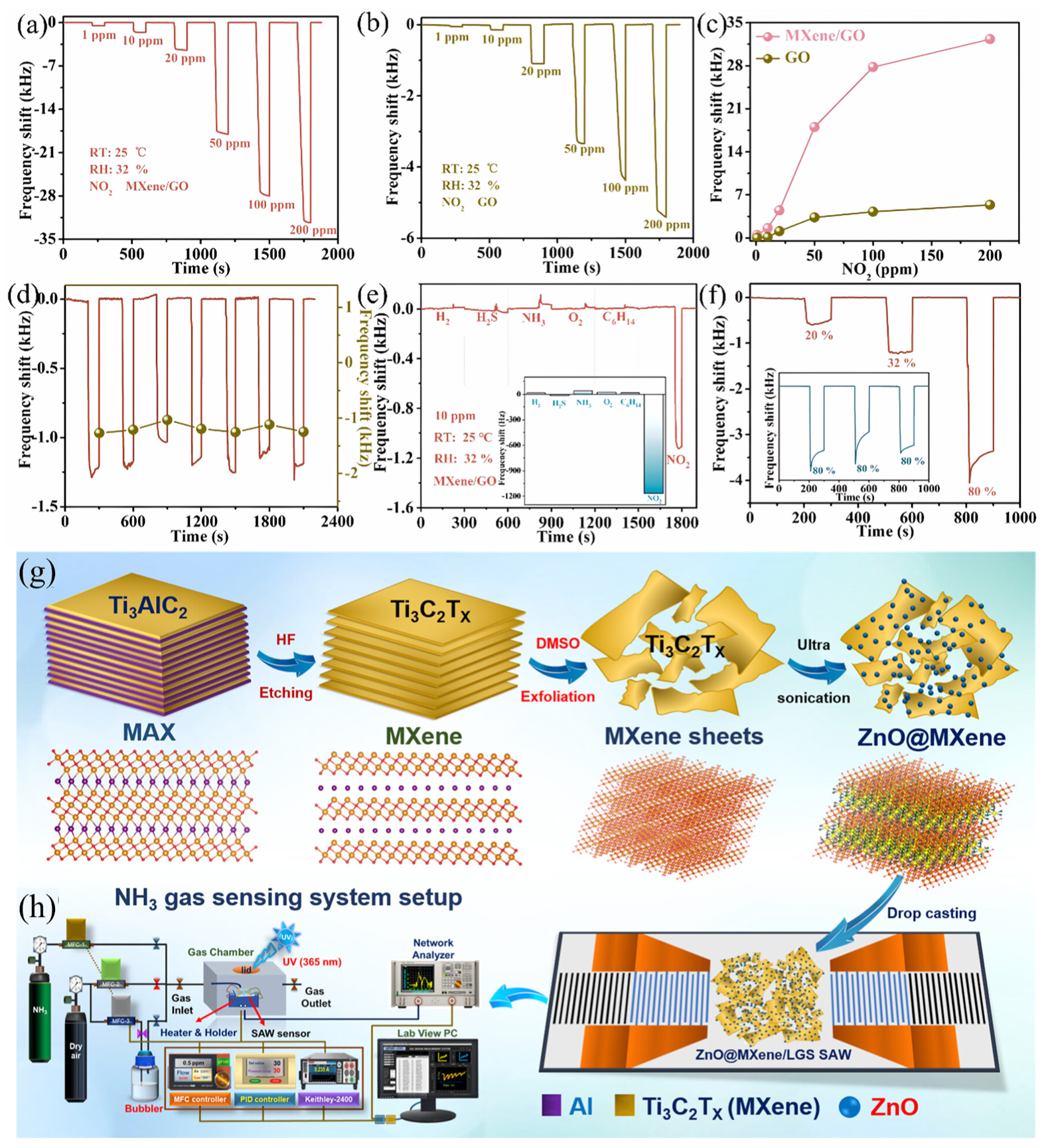
  83. Li, X.; Feng, Y.; Long, J.; Lv, H.; Guo, Y.; Zu, X. MXene-Activated Graphene Oxide Enhancing NO2 Capture and Detection of Surface Acoustic Wave Sensors. Sensors Actuat. B-Chem. 2024, 401, 135006. [Google Scholar] [CrossRef]
  84. Pasupuleti, K.S.; Thomas, A.M.; Vidyasagar, D.; Rao, V.N.; Yoon, S.-G.; Kim, Y.-H.; Kim, S.-G.; Kim, M.-D. ZnO@Ti3C2Tx MXene Hybrid Composite-Based Schottky-Barrier-Coated SAW Sensor for Effective Detection of Sub-ppb-Level NH3 at Room Temperature under UV Illumination. ACS Mater. Lett. 2023, 5, 2739–2746. [Google Scholar] [CrossRef]
  85. Glinsek, S.; Song, L.; Kovacova, V.; Mahjoub, M.A.; Godard, N.; Girod, S.; Biagi, J.-L.; Quintana, R.; Schleeh, T.; Guedra, M.; et al. Inkjet-Printed Piezoelectric Thin Films for Transparent Haptics. Adv. Mater. Tech. 2022, 7, 2200147. [Google Scholar] [CrossRef]
  86. Nikolaou, I.; Hallil, H.; Conédéra, V.; Deligeorgis, G.; Dejous, C.; Rebiere, D. Inkjet-printed graphene oxide thin layers on love wave devices for humidity and vapor detection. IEEE Sens. J. 2016, 16, 7620–7627. [Google Scholar] [CrossRef]
  87. Di, W.; Liu, F.; Lin, T.; Kong, H.; Meng, C.; Zhang, W.; Chen, Y.; Hou, Y. Influence of oxygen partial pressure on structural and electrical properties of Mn1.56Co0.96Ni0.48O4 thin films deposited by pulsed laser deposition. Appl. Surf. Sci. 2018, 447, 287–291. [Google Scholar] [CrossRef]
  88. Meng, L.; Wang, Z.; Yang, L.; Ren, W.; Liu, W.; Zhang, Z.; Yang, T.; Dos Santos, M.P. A detailed study on the Fe-doped TiO2 thin films induced by pulsed laser deposition route. Appl. Surf. Sci. 2019, 474, 211–217. [Google Scholar] [CrossRef]
  89. Viespe, C.; Miu, D. Surface Acoustic Wave Sensor with Pd/ZnO Bilayer Structure for Room Temperature Hydrogen Detection. Sensors 2017, 17, 1529. [Google Scholar] [CrossRef]
  90. Constantinoiu, I.; Viespe, C. Development of Pd/TiO2 Porous Layers by Pulsed Laser Deposition for Surface Acoustic Wave H2 Gas Sensor. Nanomaterials 2020, 10, 760. [Google Scholar] [CrossRef]
  91. Aslam, M.Z.; Zhang, H.; Sreejith, V.S.; Naghdi, M.; Ju, S. Advances in the Surface Acoustic Wave Sensors for Industrial Applications: Potentials, Challenges, and Future Directions: A Review. Measurement 2023, 222, 113657. [Google Scholar] [CrossRef]
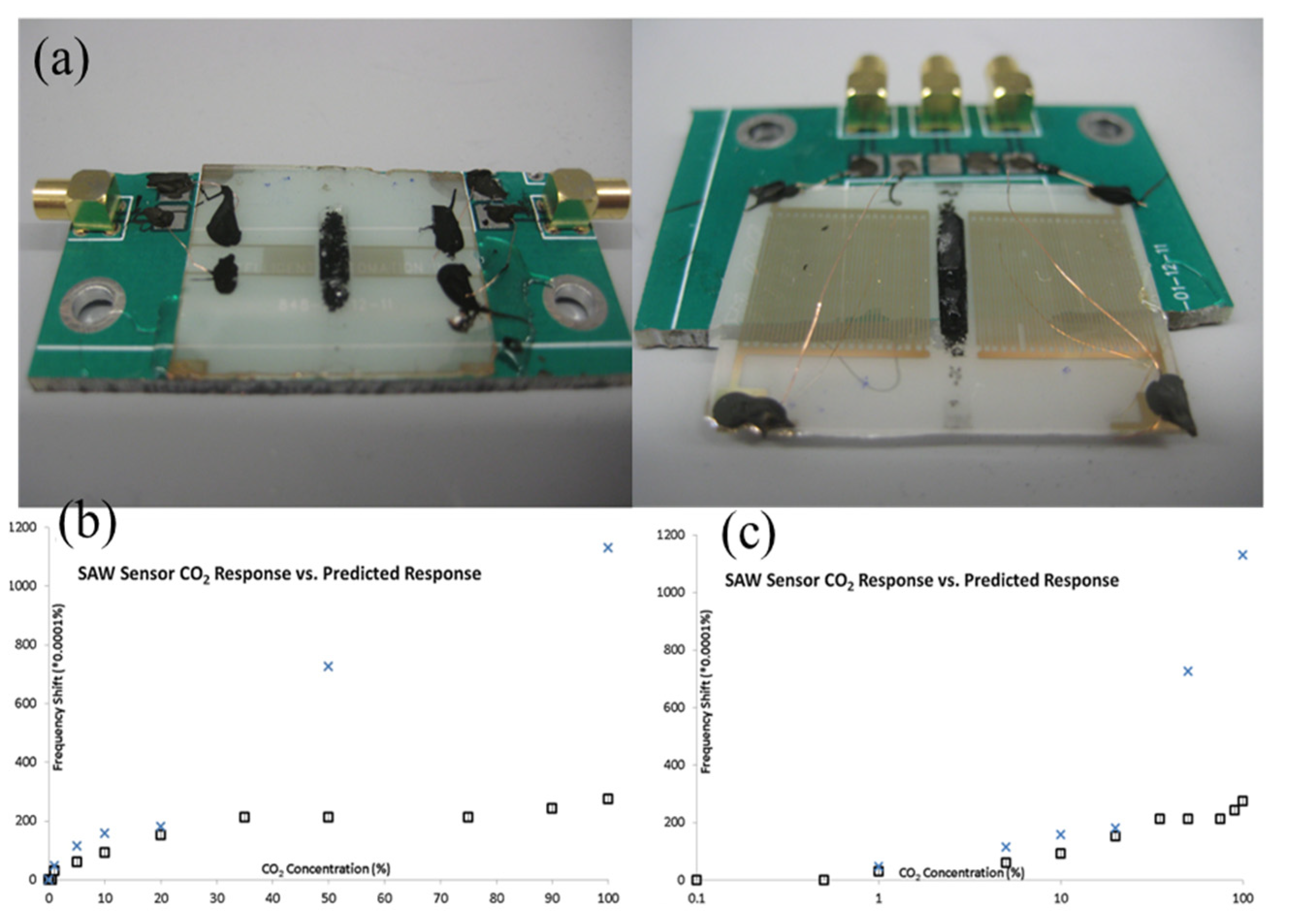
  92. Xu, S.; Li, C.; Li, H.; Li, M.; Qu, C.; Yang, B. Carbon Dioxide Sensors Based on a Surface Acoustic Wave Device with a Graphene–Nickel–L-Alanine Multilayer Film. J. Mater. Chem. C 2015, 3, 3882–3890. [Google Scholar] [CrossRef]
  93. Wang, Y.; Chyu, M.K.; Wang, Q.-M. Passive Wireless Surface Acoustic Wave CO2 Sensor with Carbon Nanotube Nanocomposite as an Interface Layer. Sens. Actuat. A-Phys. 2014, 220, 34–44. [Google Scholar] [CrossRef]
  94. Zhou, H.; Ramaraj, S.G.; Ma, K.; Sarker, M.S.; Liao, Z.; Tang, S.; Yamahara, H.; Tabata, H. Real-Time Detection of Acetone Gas Molecules at ppt Levels in an Air Atmosphere Using a Partially Suspended Graphene Surface Acoustic Wave Skin Gas Sensor. Nanoscale Adv. 2023, 5, 6999–7008. [Google Scholar] [CrossRef]
  95. Luo, W.; Fu, Q.; Zhou, D.; Deng, J.; Liu, H.; Yan, G. A Surface Acoustic Wave H2S Gas Sensor Employing Nanocrystalline SnO2 Thin Film. Sensors Actuat. B-Chem. 2013, 176, 746–752. [Google Scholar] [CrossRef]
  96. Hung, T.-T.; Chung, M.-H.; Chiu, J.-J.; Yang, M.-W.; Tien, T.-N.; Shen, C.-Y. Poly(4-Styrenesulfonic Acid) Doped Polypyrrole/Tungsten Oxide/Reduced Graphene Oxide Nanocomposite Films Based Surface Acoustic Wave Sensors for NO Sensing Behavior. Org. Electron. 2021, 88, 106006. [Google Scholar] [CrossRef]
  97. Liu, M.; Huang, X.; Song, Y.; Tang, J.; Cao, J.; Zhang, X.; Zhang, Q.; Wang, S.; Xu, T.; Kang, L.; et al. Ammonia Emission Control in China Would Mitigate Haze Pollution and Nitrogen Deposition, but Worsen Acid Rain. Proc. Natl. Acad. Sci. USA 2019, 116, 7760–7765. [Google Scholar] [CrossRef] [PubMed]
  98. Su, P.-G.; Yang, L.-Y. NH3 Gas Sensor Based on Pd/SnO2/RGO Ternary Composite Operated at Room-Temperature. Sensors Actuat. B-Chem. 2016, 223, 202–208. [Google Scholar] [CrossRef]
  99. Sun, X.; Chen, T.; Liang, Y.; Zhang, C.; Zhai, S.; Sun, J.; Wang, W. Enhanced Sensitivity of SAW Based Ammonia Sensor Employing GO-SnO2 Nanocomposites. Sensors Actuat. B-Chem. 2023, 375, 13288. [Google Scholar] [CrossRef]
  100. Mattoni, G.; de Jong, B.; Manca, N.; Tomellini, M.; Caviglia, A.D. Single-Crystal Pt-Decorated WO3 Ultrathin Films: A Platform for Sub-Ppm Hydrogen Sensing at Room Temperature. ACS Appl. Nano Mater. 2018, 1, 3446–3452. [Google Scholar] [CrossRef] [PubMed]
  101. Yunusa, Z.; Hamidon, M.N.; Ismail, A.; Isa, M.M.; Yaacob, M.H.; Rahmanian, S.; Ibrahim, S.A.; Shabaneh, A.A.A. Development of a Hydrogen Gas Sensor Using a Double Saw Resonator System at Room Temperature. Sensors 2015, 15, 4749–4765. [Google Scholar] [CrossRef] [PubMed]
  102. Jin, J.; Cui, B.; Cheng, L.; Xue, X.; Hu, A.; Liang, Y.; Wang, W. Dimensionality Regulation of ZIF Anti-Interference Layer for High-Selectivity and Fast-Response Hydrogen Sensing. Int. J. Hydrogen Energy 2024, 50, 903–911. [Google Scholar] [CrossRef]
  103. Kim, S.; Singh, G.; Lee, K. Development of Highly Sensitive and Stable Surface Acoustic Wave-Based Hydrogen Sensor and Its Interface Electronics. Adv. Mater. Technol. 2022, 7, 2200180. [Google Scholar] [CrossRef]
  104. Kim, S.S.; Kang, D.H.; Choi, D.H.; Yeo, M.S.; Kim, K.W. VOC Emission from Building Materials in Residential Buildings with Radiant Floor Heating Systems. Aerosol Air Qual. Res. 2012, 12, 1398–1408. [Google Scholar] [CrossRef]
  105. Mendell, M.J. Indoor Residential Chemical Emissions as Risk Factors for Respiratory and Allergic Effects in Children: A Review. Indoor Air 2007, 17, 259–277. [Google Scholar] [CrossRef] [PubMed]
  106. Nikolaou, I.; Hallil, H.; Dejous, C.; Rebière, D.; Deligeorgis, G.; Conedera, V. Inkjet—Printed Graphene Layer by Layer on SAW Devices for Gas Detection Applications. In Proceedings of the 2015 IEEE SENSORS, Busan, Republic of Korea, 1–4 November 2015. [Google Scholar]
  107. Li, Z.; Li, H.; Wu, Z.; Wang, M.; Luo, J.; Torun, H.; Hu, P.; Yang, C.; Grundmann, M.; Liu, X.; et al. Advances in Designs and Mechanisms of Semiconducting Metal Oxide Nanostructures for High-Precision Gas Sensors Operated at Room Temperature. Mater. Horiz. 2019, 6, 470–506. [Google Scholar] [CrossRef]
  108. Caliendo, C.; Verardi, P.; Verona, E.; D’Amico, A.; Natale, C.D.; Saggio, G.; Serafini, M.; Paolesse, R.; Huq, S.E. Advances in SAW-Based Gas Sensors. Smart Mater. Struct. 1997, 6, 689. [Google Scholar] [CrossRef]
  109. Jakubik, W.P. Surface Acoustic Wave-Based Gas Sensors. Thin Solid Films 2011, 520, 986–993. [Google Scholar] [CrossRef]
  110. Devkota, J.; Ohodnicki, P.R.; Greve, D.W. SAW Sensors for Chemical Vapors and Gases. Sensors 2017, 17, 801. [Google Scholar] [CrossRef] [PubMed]
  111. Guo, Y.J.; Long, G.D.; Tang, Y.L.; Wang, J.L.; Tang, Q.B.; Zu, X.T.; Ma, J.Y.; Du, B.; Torun, H.; Fu, Y.Q. Surface Acoustic Wave Ammonia Sensor Based on SiO2–SnO2 Composite Film Operated at Room Temperature. Smart Mater. Struct. 2020, 29, 095003. [Google Scholar] [CrossRef]
  112. Raj, V.B.; Singh, H.; Nimal, A.T.; Tomar, M.; Sharma, M.U.; Gupta, V. Effect of Metal Oxide Sensing Layers on the Distinct Detection of Ammonia Using Surface Acoustic Wave (SAW) Sensors. Sensors Actuat. B-Chem. 2013, 187, 563–573. [Google Scholar] [CrossRef]
  113. Raj, V.B.; Singh, H.; Nimal, A.T.; Sharma, M.U.; Tomar, M.; Gupta, V. Distinct Detection of Liquor Ammonia by ZnO/SAW Sensor: Study of Complete Sensing Mechanism. Sensors Actuat. B-Chem. 2017, 238, 83–90. [Google Scholar] [CrossRef]
  114. Cao, P.; Yang, Z.; Navale, S.T.; Han, S.; Liu, X.; Liu, W.; Lu, Y.; Stadler, F.J.; Zhu, D. Ethanol Sensing Behavior of Pd-Nanoparticles Decorated ZnO-Nanorod Based Chemiresistive Gas Sensors. Sensors Actuat. B-Chem. 2019, 298, 126850. [Google Scholar] [CrossRef]
  115. Huang, F.-C.; Chen, Y.-Y.; Wu, T.-T. A Room Temperature Surface Acoustic Wave Hydrogen Sensor with Pt Coated ZnO Nanorods. Nanotechnology 2009, 20, 065501. [Google Scholar] [CrossRef]
  116. Abraham, N.; Reshma Krishnakumar, R.; Unni, C.; Philip, D. Simulation Studies on the Responses of ZnO-CuO/CNT Nanocomposite Based SAW Sensor to Various Volatile Organic Chemicals. J. Sci. Adv. Mater. Devices 2019, 4, 125–131. [Google Scholar] [CrossRef]
  117. Li, M.; Kan, H.; Chen, S.; Feng, X.; Li, H.; Li, C.; Fu, C.; Quan, A.; Sun, H.; Luo, J.; et al. Colloidal Quantum Dot-Based Surface Acoustic Wave Sensors for NO2-Sensing Behavior. Sensors Actuat. B-Chem. 2019, 287, 241–249. [Google Scholar] [CrossRef]
  118. Wen, C.; Zhu, C.; Ju, Y.; Xu, H.; Qiu, Y. A Novel NO2 Gas Sensor Using Dual Track SAW Device. Sens. Actuat. A-Phys. 2010, 159, 168–173. [Google Scholar] [CrossRef]
  119. Pasupuleti, K.S.; Reddeppa, M.; Chougule, S.S.; Bak, N.H.; Nam, D.J.; Jung, N.; Cho, H.D.; Kim, S.G.; Kim, M.D. High Performance Langasite Based SAW NO2 Gas Sensor Using 2D G-C3N4@TiO2 Hybrid Nanocomposite. J. Hazard. Mater. 2022, 427, 128174. [Google Scholar] [CrossRef] [PubMed]
  120. Lee, M.E.; Armani, A.M. Flexible UV Exposure Sensor Based on UV Responsive Polymer. ACS Sens. 2016, 1, 1251–1255. [Google Scholar] [CrossRef]
  121. Wang, W.-S.; Wu, T.-T.; Chou, T.-H.; Chen, Y.-Y. A ZnO Nanorod-Based SAW Oscillator System for Ultraviolet Detection. Nanotechnology 2009, 20, 135503. [Google Scholar] [CrossRef]
  122. Guo, Y.; Yin, C.; Zhou, J.; Ji, Z.; Zhuo, F.; Ong, H.L.; Zhang, J.; Duan, H.; Fu, R. Decoupling Acoustoelectric and Thermal Effects of Ultraviolet Responses for Acoustic Wave Sensing Mechanisms. IEEE Sens. J. 2023, 23, 11444–11452. [Google Scholar] [CrossRef]
  123. Fu, C.; Lee, K.J.; Lee, K.; Yang, S.S. Low-Intensity Ultraviolet Detection Using a Surface Acoustic-Wave Sensor with a Ag-Doped ZnO Nanoparticle Film. Smart Mater. Struct. 2014, 24, 015010. [Google Scholar] [CrossRef]
  124. Yu, X.; Xie, C.; Yang, L.; Zhang, S. Highly Photoactive Sensor Based on NiO Modified TiO2 Porous Film for Diethyl Ether. Sensors Actuat. B-Chem. 2014, 195, 439–445. [Google Scholar] [CrossRef]
  125. Han, Y.; Fan, C.; Wu, G.; Chen, H.-Z.; Wang, M. Low-Temperature Solution Processed Utraviolet Photodetector Based on an Ordered TiO2 Nanorod Array–Polymer Hybrid. J. Phys. Chem. C 2011, 115, 13438–13445. [Google Scholar] [CrossRef]
  126. Xie, Y.; Wei, L.; Li, Q.; Chen, Y.; Yan, S.; Jiao, J.; Liu, G.; Mei, L. High-Performance Self-Powered UV Photodetectors Based on TiO2 Nano-Branched Arrays. Nanotechnology 2014, 25, 075202. [Google Scholar] [CrossRef] [PubMed]
  127. Water, W.; Wen, C.-W. Application of TiO2 Thin Film with Nanorods to Surface Acoustic Wave Type Ultraviolet Photo Detection. J. Electroceram. 2016, 36, 94–101. [Google Scholar] [CrossRef]
  128. He, X.L.; Li, D.J.; Zhou, J.; Wang, W.B.; Xuan, W.P.; Dong, S.R.; Jin, H.; Luo, J.K. High Sensitivity Humidity Sensors Using Flexible Surface Acoustic Wave Devices Made on Nanocrystalline ZnO/Polyimide Substrates. J. Mater. Chem. C 2013, 1, 6210–6215. [Google Scholar] [CrossRef]
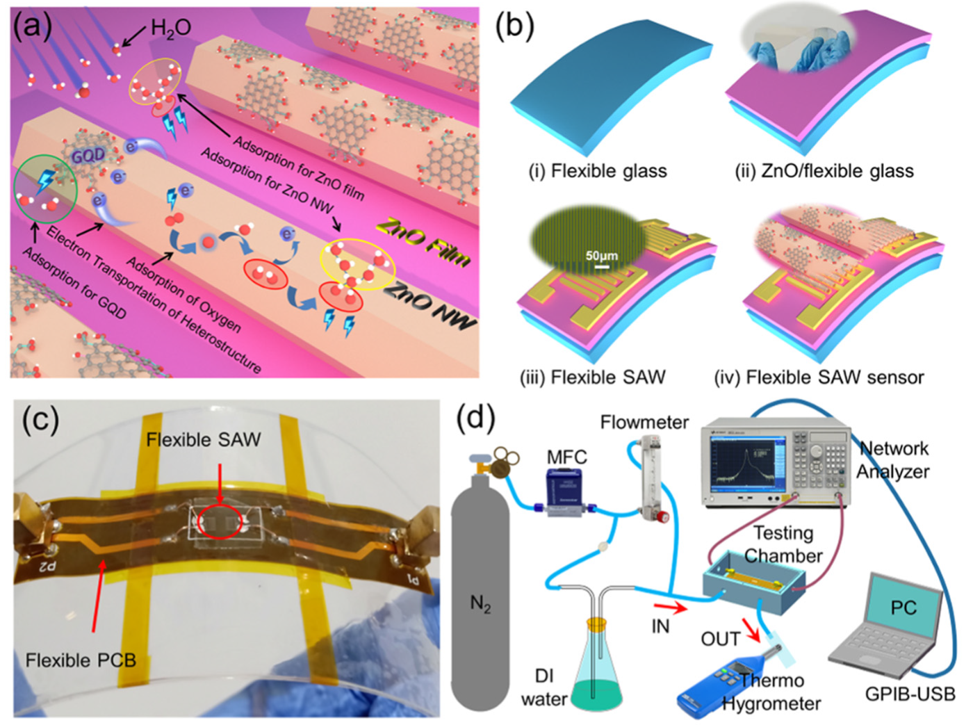
  129. Wu, J.; Yin, C.; Zhou, J.; Li, H.; Liu, Y.; Shen, Y.; Garner, S.; Fu, Y.; Duan, H. Ultrathin Glass-Based Flexible, Transparent, and Ultrasensitive Surface Acoustic Wave Humidity Sensor with ZnO Nanowires and Graphene Quantum Dots. ACS Appl. Mater. Interfaces 2020, 12, 39817–39825. [Google Scholar] [CrossRef]
  130. Traversa, E. Ceramic Sensors for Humidity Detection: The State-of-the-Art and Future Developments. Sensors Actuat. B-Chem. 1995, 23, 135–156. [Google Scholar] [CrossRef]
  131. Alizadeh, T.; Shokri, M. A New Humidity Sensor Based upon Graphene Quantum Dots Prepared via Carbonization of Citric Acid. Sensors Actuat. B-Chem. 2016, 222, 728–734. [Google Scholar] [CrossRef]
  132. Su, Y.; Li, C.; Li, M.; Li, H.; Xu, S.; Qian, L.; Yang, B. Surface Acoustic Wave Humidity Sensor Based on Three-Dimensional Architecture Graphene/PVA/SiO2 and Its Application for Respiration Monitoring. Sensors Actuat. B-Chem. 2020, 308, 127693. [Google Scholar] [CrossRef]
  133. Le, X.; Liu, Y.; Peng, L.; Pang, J.; Xu, Z.; Gao, C.; Xie, J. Surface Acoustic Wave Humidity Sensors Based on Uniform and Thickness Controllable Graphene Oxide Thin Films Formed by Surface Tension. Microsyst. Nanoeng. 2019, 5, 36. [Google Scholar] [CrossRef]
  134. Xuan, W.; He, X.; Chen, J.; Wang, W.; Wang, X.; Xu, Y.; Xu, Z.; Fu, Y.Q.; Luo, J.K. High Sensitivity Flexible Lamb-Wave Humidity Sensors with a Graphene Oxide Sensing Layer. Nanoscale 2015, 7, 7430–7436. [Google Scholar] [CrossRef]
  135. Le, X.; Wang, X.; Pang, J.; Liu, Y.; Fang, B.; Xu, Z.; Gao, C.; Xu, Y.; Xie, J. A High Performance Humidity Sensor Based on Surface Acoustic Wave and Graphene Oxide on AlN/Si Layered Structure. Sensors Actuat. B-Chem. 2018, 255, 2454–2461. [Google Scholar] [CrossRef]
  136. Liu, Y.; Huang, H.; Wang, L.; Cai, D.; Liu, B.; Wang, D.; Li, Q.; Wang, T. Electrospun CeO2 Nanoparticles/PVP Nanofibers Based High-Frequency Surface Acoustic Wave Humidity Sensor. Sensors Actuat. B-Chem. 2016, 223, 730–737. [Google Scholar] [CrossRef]
  137. Li, C.; Zhang, J.; Xie, H.; Luo, J.; Fu, C.; Tao, R.; Li, H.; Fu, Y. Highly Sensitive Love Mode Acoustic Wave Platform with SiO2 Wave-Guiding Layer and Gold Nanoparticles for Detection of Carcinoembryonic Antigens. Biosensors 2022, 12, 536. [Google Scholar] [CrossRef]
  138. Jandas, P.J.; Luo, J.; Prabakaran, K.; Chen, F.; Fu, Y.Q. Highly Stable, Love-Mode Surface Acoustic Wave Biosensor Using Au Nanoparticle-MoS2-rGO Nano-Cluster Doped Polyimide Nanocomposite for the Selective Detection of Carcinoembryonic antigen. Mater. Chem. Phys. 2020, 246, 122800. [Google Scholar] [CrossRef]
  139. Feng, B.; Zhao, K.; Su, Q.; Yu, Z.; Jin, H. Passive Wireless Respiratory Sensor. Electron. Lett. 2021, 57, 730–731. [Google Scholar] [CrossRef]
  140. Chang, K.; Pi, Y.; Lu, W.; Wang, F.; Pan, F.; Li, F.; Jia, S.; Shi, J.; Deng, S.; Chen, M. Label-Free and High-Sensitive Detection of Human Breast Cancer Cells by Aptamer-Based Leaky Surface Acoustic Wave Biosensor Array. Biosens. Bioelectron. 2014, 60, 318–324. [Google Scholar] [CrossRef]
  141. Trivedi, S.; Nemade, H.B. Coupled Resonance in SH-SAW Resonator with S1813 Micro-Ridges for High Mass Sensitivity Biosensing Applications. Sensors Actuat. B-Chem. 2018, 273, 288–297. [Google Scholar] [CrossRef]
  142. Turbé, V.; Gray, E.R.; Lawson, V.E.; Nastouli, E.; Brookes, J.C.; Weiss, R.A.; Pillay, D.; Emery, V.C.; Verrips, C.T.; Yatsuda, H.; et al. Towards an Ultra-Rapid Smartphone- Connected Test for Infectious Diseases. Sci. Rep. 2017, 7, 11971. [Google Scholar] [CrossRef]
  143. Marcaccio, M.; Paolucci, F. Making and Exploiting Fullerenes, Graphene, and Carbon Nanotubes, 1st ed.; Springer: Berlin/Heidelberg, Germany, 2014; pp. 237–265. [Google Scholar]
  144. Suvarnaphaet, P.; Pechprasarn, S. Graphene-Based Materials for Biosensors: A Review. Sensors 2017, 17, 2161. [Google Scholar] [CrossRef]
  145. Ye, Y.; Xie, J.; Ye, Y.; Cao, X.; Zheng, H.; Xu, X.; Zhang, Q. A Label-Free Electrochemical DNA Biosensor Based on Thionine Functionalized Reduced Graphene Oxide. Carbon 2018, 129, 730–737. [Google Scholar] [CrossRef]
  146. Mogha, N.K.; Sahu, V.; Sharma, R.K.; Masram, D.T. Reduced Graphene Oxide Nanoribbon Immobilized Gold Nanoparticle Based Electrochemical DNA Biosensor for the Detection of Mycobacterium Tuberculosis. J. Mater. Chem. B 2018, 6, 5181–5187. [Google Scholar] [CrossRef]
  147. Primo, E.N.; Kogan, M.J.; Verdejo, H.E.; Bollo, S.; Rubianes, M.D.; Rivas, G.A. Label-Free Graphene Oxide-Based Surface Plasmon Resonance Immunosensor for the Quantification of Galectin-3, a Novel Cardiac Biomarker. ACS Appl. Mater. Interfaces 2018, 10, 23501–23508. [Google Scholar] [CrossRef]
  148. Hur, Y.; Han, J.; Seon, J.; Pak, Y.E.; Roh, Y. Development of an SH-SAW Sensor for the Detection of DNA Hybridization. Sens. Actuat. A-Phys. 2005, 120, 462–467. [Google Scholar] [CrossRef]
  149. Gizeli, E.; Bender, F.; Rasmusson, A.; Saha, K.; Josse, F.; Cernosek, R. Sensitivity of the Acoustic Waveguide Biosensor to Protein Binding as a Function of the Waveguide Properties. Biosens. Bioelectron. 2003, 18, 1399–1406. [Google Scholar] [CrossRef] [PubMed]
  150. Ji, J.; Pang, Y.; Li, D.; Wang, X.; Xu, Y.; Mu, X. Single-Layered Graphene/Au-Nanoparticles-Based Love Wave Biosensor for Highly Sensitive and Specific Detection of Staphylococcus Aureus Gene Sequences. ACS Appl. Mater. Interfaces 2020, 12, 12417–12425. [Google Scholar] [CrossRef] [PubMed]
  151. Song, Y.; Xu, T.; Xu, L.-P.; Zhang, X. Nanodendritic Gold/Graphene-Based Biosensor for Tri-Mode miRNA Sensing. Chem. Commun. 2019, 55, 1742–1745. [Google Scholar] [CrossRef] [PubMed]
  152. Hernández-Sánchez, D.; Villabona-Leal, G.; Saucedo-Orozco, I.; Bracamonte, V.; Pérez, E.; Bittencourt, C.; Quintana, M. Stable Graphene Oxide–Gold Nanoparticle Platforms for Biosensing Applications. Phys. Chem. Chem. Phys. 2018, 20, 1685–1692. [Google Scholar] [CrossRef] [PubMed]
  153. Wang, J.; Han, H.; Jiang, X.; Huang, L.; Chen, L.; Li, N. Quantum Dot-Based Near-Infrared Electrochemiluminescent Immunosensor with Gold Nanoparticle-Graphene Nanosheet Hybrids and Silica Nanospheres Double-Assisted Signal Amplification. Anal. Chem. 2012, 84, 4893–4899. [Google Scholar] [CrossRef] [PubMed]
  154. Tang, X.; Bansaruntip, S.; Nakayama, N.; Yenilmez, E.; Chang, Y.; Wang, Q. Carbon Nanotube DNA Sensor and Sensing Mechanism. Nano Lett. 2006, 6, 1632–1636. [Google Scholar] [CrossRef]
  155. Chen, R.J.; Choi, H.C.; Bangsaruntip, S.; Yenilmez, E.; Tang, X.; Wang, Q.; Chang, Y.-L.; Dai, H. An Investigation of the Mechanisms of Electronic Sensing of Protein Adsorption on Carbon Nanotube Devices. J. Am. Chem. Soc. 2004, 126, 1563–1568. [Google Scholar] [CrossRef]
  156. Chen, R.J.; Bangsaruntip, S.; Drouvalakis, K.A.; Wong Shi Kam, N.; Shim, M.; Li, Y.; Kim, W.; Utz, P.J.; Dai, H. Noncovalent Functionalization of Carbon Nanotubes for Highly Specific Electronic Biosensors. Proc. Natl. Acad. Sci. USA 2003, 100, 4984–4989. [Google Scholar] [CrossRef]
  157. Wu, H.; Zu, H.; Wang, Q.-M.; Zhao, G.; Wang, J.H.-C. Label-Free Detection of Protein Released during Platelet Activation by CNT-Enhanced Love Mode SAW Sensors. IEEE Int. Ultrason. Symp. 2014, 2014, 1528–1531. [Google Scholar]
  158. Pasupuleti, K.S.; Reddeppa, M.; Nam, D.-J.; Bak, N.-H.; Peta, K.R.; Cho, H.D.; Kim, S.-G.; Kim, M.-D. Boosting of NO2 Gas Sensing Performances Using GO-PEDOT:PSS Nanocomposite Chemical Interface Coated on Langasite-Based Surface Acoustic Wave Sensor. Sensors Actuat. B-Chem. 2021, 344, 130267. [Google Scholar] [CrossRef]
  159. Barroso-Bujans, F.; Cerveny, S.; Alegría, A.; Colmenero, J. Sorption and Desorption Behavior of Water and Organic Solvents from Graphite Oxide. Carbon 2010, 48, 3277–3286. [Google Scholar] [CrossRef]
  160. Tang, Q.B.; Guo, Y.J.; Tang, Y.L.; Long, G.D.; Wang, J.L.; Li, D.J.; Zu, X.T.; Ma, J.Y.; Wang, L.; Torun, H.; et al. Highly Sensitive and Selective Love Mode Surface Acoustic Wave Ammonia Sensor Based on Graphene Oxides Operated at Room Temperature. J. Mater. Sci. 2019, 54, 11925–11935. [Google Scholar] [CrossRef]
  161. Cheng, C.-Y.; Huang, S.-S.; Yang, C.-M.; Tang, K.-T.; Yao, D.-J. Detection of Cigarette Smoke Using a Surface-Acoustic-Wave Gas Sensor with Non-Polymer-Based Oxidized Hollow Mesoporous Carbon Nanospheres. Micromachines 2019, 10, 276. [Google Scholar] [CrossRef]
  162. Sayago, I.; Matatagui, D.; Fernández, M.J.; Fontecha, J.L.; Jurewicz, I.; Garriga, R.; Muñoz, E. Graphene Oxide as Sensitive Layer in Love-Wave Surface Acoustic Wave Sensors for the Detection of Chemical Warfare Agent Simulants. Talanta 2016, 148, 393–400. [Google Scholar] [CrossRef]
  163. Tan, K.; Ji, Z.; Zhou, J.; Deng, Z.; Zhang, S.; Gu, Y.; Guo, Y.; Zhuo, F.; Duan, H.; Fu, Y. Machine Learning Empowered Thin Film Acoustic Wave Sensing. Appl. Phys. Lett. 2023, 122, 014101. [Google Scholar] [CrossRef]
Figure 1. The main application of a SAW sensor based on low-dimensional materials.
Chemosensors 12 00255 g001
Figure 2. The type of SAW: (a) delay line type; (b) resonator type.
Chemosensors 12 00255 g002
Figure 3. (a) The schematic and a photograph of the SAW NO2 sensor based on SnS colloidal QDs. (b) The response curves of the SAW sensor to different NO2 concentrations. (c) The selectivity of the sensor. Reproduced with permission from [62] (Copyright 2019, Elsevier). The schematic diagram (d) and photograph (e) of a flexible SAW UV sensor using GQDs@ZnO-NWs composite nanomaterials. (f) Repeatability testing results of devices with and without a GQDs@ZnO-NWs sensitive layer under a light intensity of 50 mW/cm2. Device response time and recovery time when a UV light is turned on and off with (g) and without (h) a GQDs@ZnO-NWs sensitive layer. Reproduced with permission from [64] (Copyright 2021, Elsevier).
Chemosensors 12 00255 g003
Figure 4. (a) An optical picture of the developed sensing device, (b) an SEM view of Pd/Cu nanorods, and (c) the measured S21 of the sensing device before and after Pd/Cu deposition. Reproduced with permission from [71] (Copyright 2019, Elsevier).
Chemosensors 12 00255 g004
Figure 5. (a) Schematic structure of a ZnO/glass-based single port SAW resonator packaged on a coplanar waveguide substrate. (b) A packaged SAW resonator; (c) an SEM image of a SAW resonator; (d) the 12 m and (e) 1 m spatial resolution of SEM images of IDT structures. Reproduced with permission from [80] (Copyright 2017, Elsevier).
Chemosensors 12 00255 g005
Figure 6. The dynamic NO2 gas-sensing frequency responses (Δf) of (a) an MXene/GO composite, (b) GO, and (c) the summary and comparation of Δf. (d) Cycling stability test of the MXene/GO SAW sensor for NO2 for a short time. (e) Selectivity test of the MXene/GO SAW sensor (inset: bar chart of selectivity). (f) Dynamic frequency shifts in the MXene/GO SAW sensor for NO2 under different relative humidity (inset: cycling stability of the MXene/GO SAW sensor). Reproduced with permission from [83] (Copyright 2024, Elsevier). (g) Schematic illustration of the material synthesis process for the fabrication of a ZnO@MXene hybrid heterostructure-based SAW sensor. (h) Schematic depiction of the experimental NH3 gas-sensing system setup. Reproduced with permission from [84] (Copyright 2023, American Chemical Society).
Chemosensors 12 00255 g006
Figure 7. (a) A photograph of passive wireless SAW CO2 sensor based on CNTs thin film; (b,c) sensor performance of the SAW CO2 sensor. Reproduced with permission from [93] (Copyright 2014, Elsevier).
Chemosensors 12 00255 g007
Figure 9. (a) A schematic illustration of the adsorption mechanism of H2O molecules on the composite sensing layer. (b) A schematic diagram of the fabrication process for the SAW sensor based on ZnO NWs and GQDs. (c) A device packaged on a polyimide flexible printed circuit board (PCB) and mounted on 1 mm thick poly (ethylene terephthalate) (PET). (d) Schematic view of the testing system used for humidity sensing. Reproduced with permission from [129] (Copyright 2020, American Chemical Society).
Chemosensors 12 00255 g009
Figure 10. (a) Schematic diagram of the fabrication process for the SAW sensor based on 3DAG/PVA/SiO2. (b) Sensing mechanism of the SAW humidity sensors coated with the 3DAG/PVA/SiO2 film. Reproduced with permission from [132] (Copyright 2020, Elsevier).
Chemosensors 12 00255 g010
Figure 11. (a) A schematic illustration and photos of the CEA measurement system based on a Love-mode SAW device; reproduced with permission from [137] (Copyright 2022, MDPI). (b) Schematic diagraph of a SAW biosensor for the selective detection of CEA using a transuding polymer-nanocomposite-thin-film-based bioreceptor; reproduced with permission from [138] (Copyright 2020, Elsevier). (c) The experimental setup for the measurement of the response and recovery time of the passive wireless respiratory sensor. (d) Resonance frequency shift in the SAW sensor during a deep breath; reproduced with permission from [139] (Copyright 2021, John Wiley and Sons).
Chemosensors 12 00255 g011
Table 1. The main performance parameters of commonly used piezoelectric materials [25,44].
MaterialsZnOAlNST-Cut QuartzGaN128° Cut LiNbO336° YX cut LiTaO3PVDF
Density (103 kg/m3)5.61–5.723.25–3.32.656.095–6.154.647.451.78
Young’s modulus (GPa)110–140300–35071.7320130–1702052.5
Poisson’s ratio0.360.22–0.290.17–0.20.1830.24–0.280.17–0.20.33–0.4
Refractive index1.9–2.01.961.462.3–2.52.292.181.42
Piezo-constant d33 (pC/N)124.5, 6.42.3 (d11)4.51212−35
Effective coupling coefficient, k2 (%)1.5–1.73.1–80.1–0.20.135–11.35–6.62.9
Acoustic velocity of longitudinal (transverse) waves (m/s)6336 (2720)10,150–11,050 (5800)5000–5960 (3159)8050 (4130)3680–39804160–42202600
Dielectric constant8.668.5–104.3~85 (29)54 (43)6–8
TCF (ppm/°C)−40 to −60−19 to −25028.375−30
Coefficient of thermal expansion (CTE, ×10−6)4–6.55.21.53.1715−16.542–75
Inherent material loss(dB·cm−1)2.25 (600 MHz)~0.85–0.95 (1000 MHz)~0.26–0.31 (1000 MHz)0.35 (1000 MHz)~
CMOS compatibleIncompatibleCompatibleCompatible~Compatible~~
Table 2. Characteristics of different types of SAWs [13].
Wave TypeCommonly Used SubstrateOperational Frequency RangeAttenuationAdvantages
Rayleigh Wave
  • 128° YX lithium niobate
  • 41° YX lithium niobate
  • ST-Quartz
  • ~3 MHz–~2 GHz
  • Most application 345 MHz
  • High attenuation.
  • Attenuation is significantly large, with the fluid load gathering on the top of the substrate.
  • Low power consumption for wave generation.
  • Low cost.
Lamb Wave
  • ZnO thin film
  • AlN thin film
  • PVDF thin film
  • ~200–~2 MHz in natural materials
  • 200 MHz–2 GHz in artificially made thin films
  • Low attenuation.
  • In presence of liquid load on the substrate, leaky-Lamb wave propagates.
  • Leaky waves attenuate faster.
  • First antisymmetric (A0) and first symmetric (S0) wave modes are easy to detect with appropriate delay lines.
SH-Wave
  • 64° YX lithium niobate
  • 36° YX lithium niobate
  • Quartz
  • ~100–~450 MHz
  • Non-dispersive.
  • Low attenuation; however, sometimes it can be challenging to detect due to potential interference from bulk waves.
  • Low cost.
  • Wide application.
  • Suitable for fluid environment.
Love Wave
  • Substrates: Similar to SH-wave
  • Guiding layers: SiO2, ZnO, TiO2, SU-8 photoresists, polymethyl methacrylate etc.
  • ~100–~450 MHz same as SH wave
  • The insertion loss increases with the increase in coating thickness.
  • The attenuation in the guiding layer or the coating layer has a significant impact.
  • Highly sensitive.
  • Works in the fluid loading environment.
Table 3. Comparison of coating techniques for low-dimensional materials in SAW devices.
Coating TechniqueApplicable MaterialsFilm Thickness ControlCostTemperature RequirementsAdvantagesDisadvantages
Spin CoatingWide range of materialsModerate control through solution concentration and spin parametersInexpensiveRoom temperatureSimple, high reproducibility, low costLimited to flat substrates, material wastage
Inkjet printingSpecially designed inksPrecise control through ink concentration, drop volume, and printing patternsInexpensiveRoom temperatureDigital patterning, material efficiency, compatible with various substratesStrict ink requirements, nozzle clogging, limited film thickness
CVDWide range of materialsExcellent control through precursor flow rates, reaction conditionsModerate600–1000 °CHigh-quality films, large-area deposition, controllable thickness and compositionHigh temperatures, complex process control
PLDSuitable for all types of material phasesExcellent control through laser fluence, deposition timeExpensiveRoom temperature to high temperatureHigh-quality epitaxial films, stoichiometry transfer, low-temperature growth possibleLimited deposition area
Disclaimer/Publisher’s Note: The statements, opinions and data contained in all publications are solely those of the individual author(s) and contributor(s) and not of MDPI and/or the editor(s). MDPI and/or the editor(s) disclaim responsibility for any injury to people or property resulting from any ideas, methods, instructions or products referred to in the content.

