
High-Sensitivity H2 and CH4 SAW Sensors with Carbon Nanowalls and Improvement in Their Performance after Plasma Treatment

 ,
,  , , and
Abstract
:1. Introduction
2. Materials and Methods
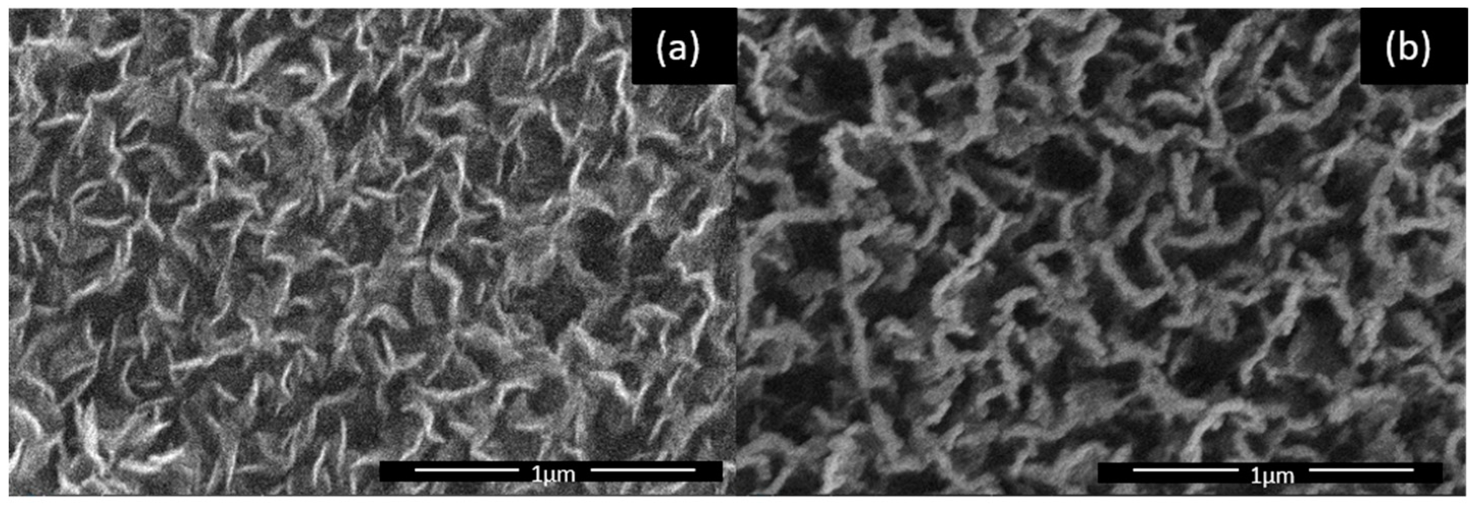
2.1. Synthesis of CNWs and Their Plasma Treatment
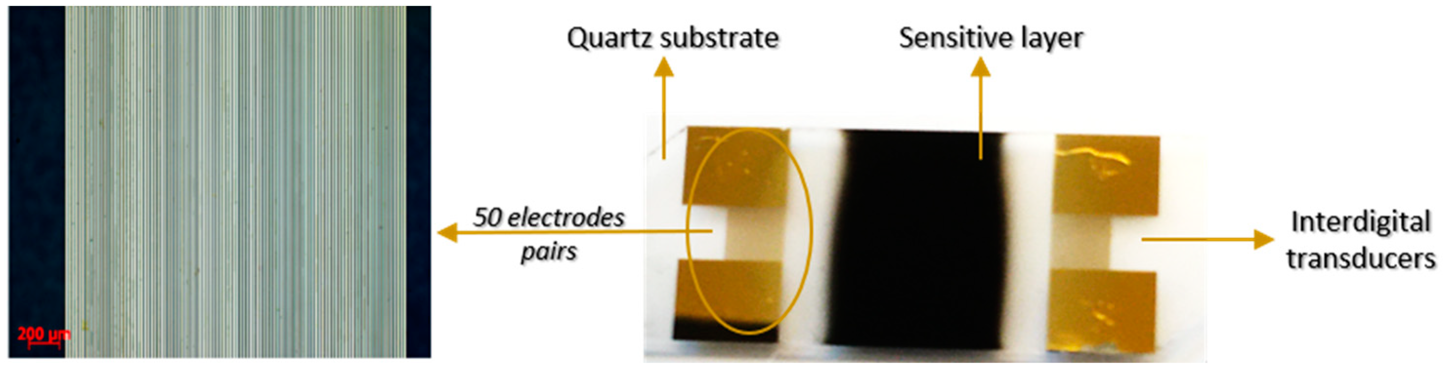
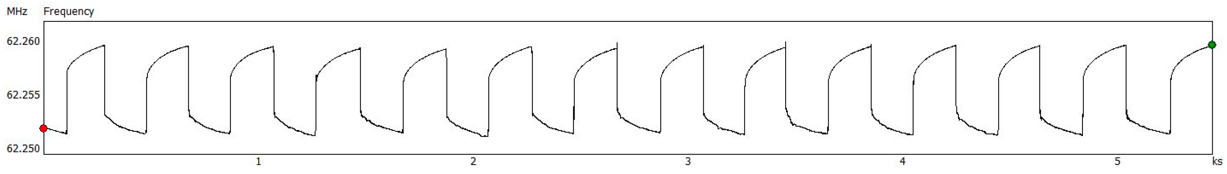
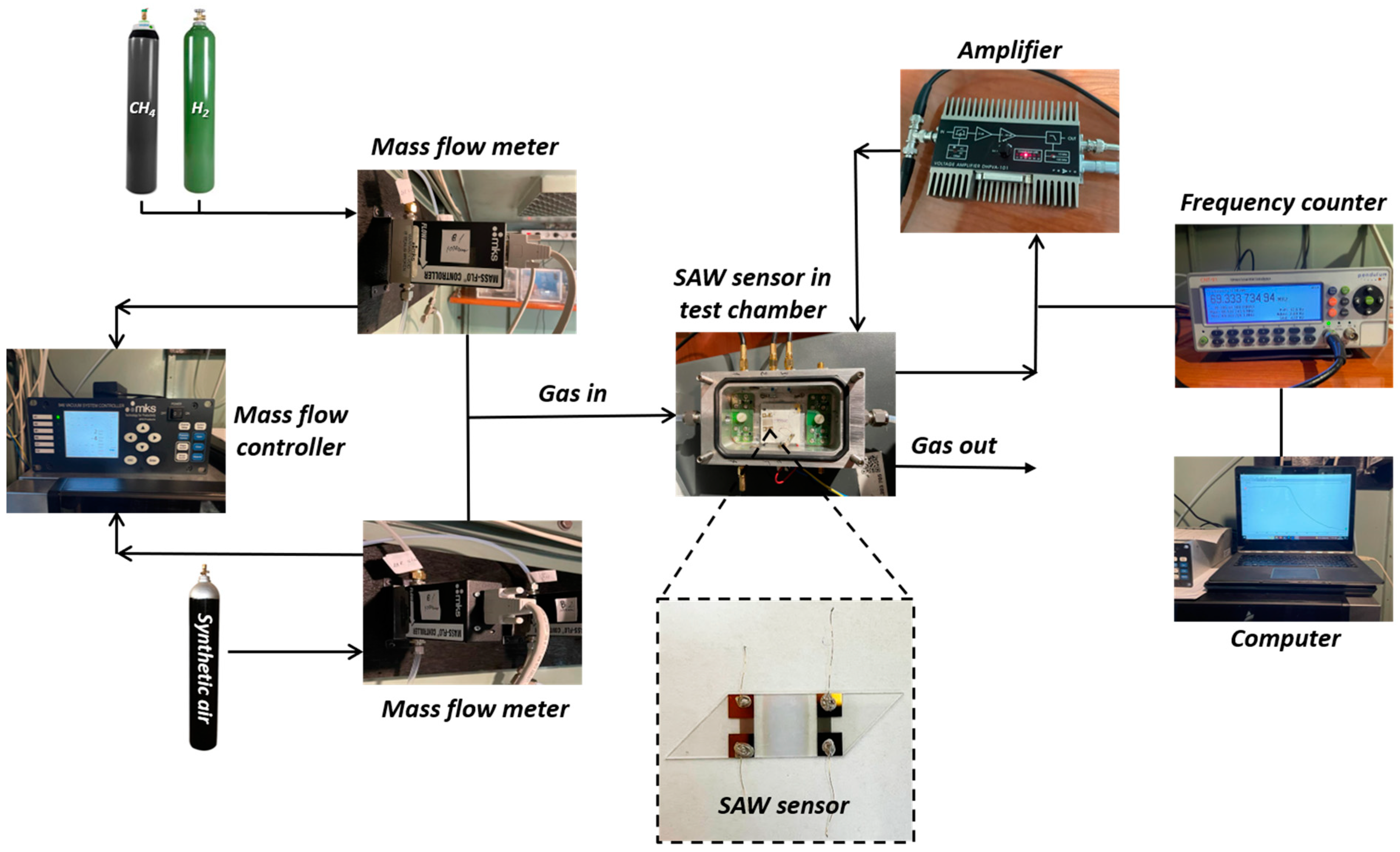
2.2. Sensor Structure and Testing
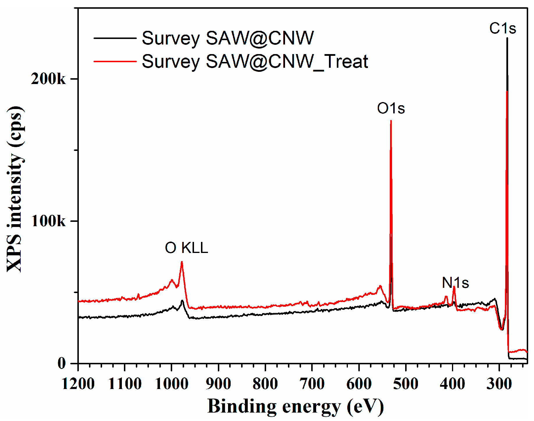
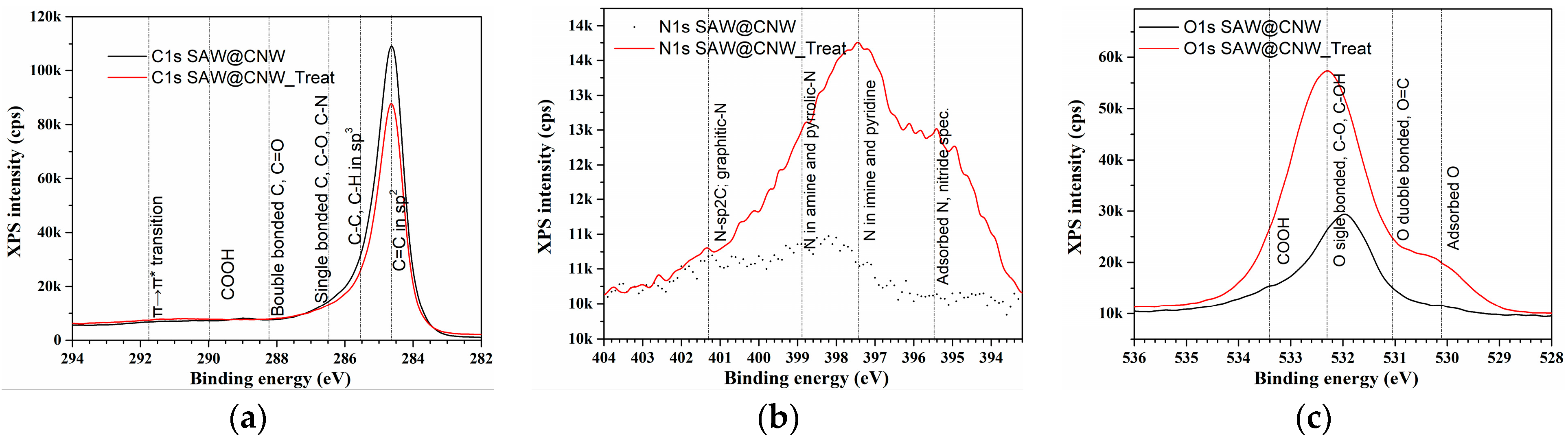
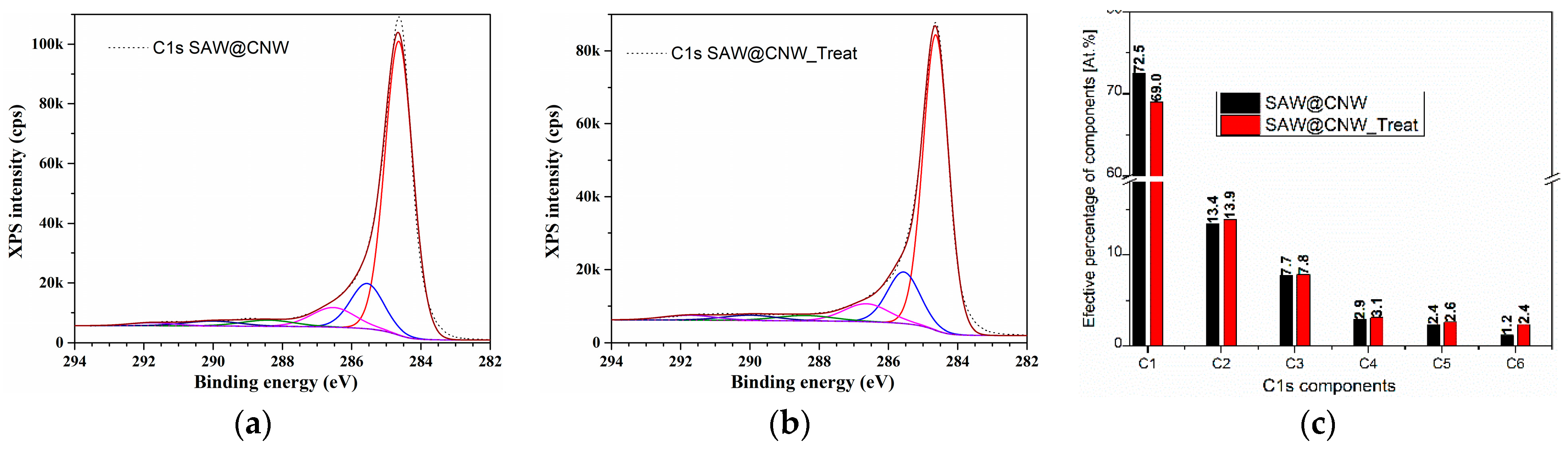
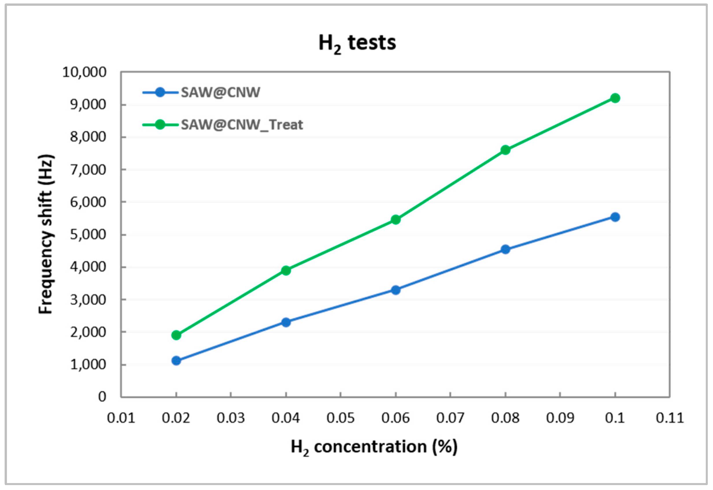
3. Results and Discussion
4. Conclusions
Author Contributions
Funding
Institutional Review Board Statement
Informed Consent Statement
Data Availability Statement
Conflicts of Interest
References
- Constantinoiu, I.; Viespe, C. Detection of Volatile Organic Compounds Using Surface Acoustic Wave Sensor Based on Nanoparticles Incorporated in Polymer. Coatings 2019, 9, 373. [Google Scholar] [CrossRef]
- Constantinoiu, I.; Viespe, C. Development of Pd/TiO2 Porous Layers by Pulsed Laser Deposition for Surface Acoustic Wave H2 Gas Sensor. Nanomaterials 2020, 10, 760. [Google Scholar] [CrossRef] [PubMed]
- Pan, Y.; Wang, P.; Zhang, G.; Yan, C.; Zhang, L.; Guo, T.; Wang, W.; Zhai, S. Development of a SAW poly(epichlorohydrin) gas sensor for detection of harmful chemicals. Anal. Methods 2022, 14, 1611. [Google Scholar] [PubMed]
- Li, Y.; Xiao, A.S.; Zou, B.; Zhang, H.X.; Yan, K.L.; Lin, Y. Advances of metal–organic frameworks for gas sensing. Polyhedron 2018, 154, 83–97. [Google Scholar]
- Mandal, D.; Banerjee, S. Surface Acoustic Wave (SAW) Sensors: Physics, Materials and Applications. Sensors 2022, 22, 820. [Google Scholar]
- Zhao, L.; Che, J.; Cao, Q.; Shen, S.; Tang, Y. Highly Sensitive Surface Acoustic Wave H2S Gas Sensor Using Electron-beam-evaporated CuO as Sensitive Layer. Sens. Mater. 2023, 35, 2293–2304. [Google Scholar]
- Longa, G.; Guoa, Y.; Lib, W.; Tanga, Q.; Zua, X.; Mac, J.; Duc, B.; Fud, Y. Surface acoustic wave ammonia sensor based on ZnS mucosal-like nanostructures. Microelectron. Eng. 2020, 222, 111201. [Google Scholar]
- Li, H.; Li, M.; Kan, H.; Lia, C.; Quan, A.; Fu, C.; Luo, J.; Liu, X.; Wang, W.; Yang, Z.; et al. Surface acoustic wave NO2 sensors utilizing colloidal SnS quantum dot thin films. Surf. Coat. Technol. 2019, 362, 78–83. [Google Scholar]
- Arsat, R.; Breedon, M.; Shafiei, M.; Spizziri, P.G.; Gilje, S.; Kaner, R.B.; Kalantar-Zadeh, K.; Wlodarski, W. Graphene-like nano-sheets for surface acoustic wave gas sensor applications. Chem. Phys. Lett. 2009, 467, 344–347. [Google Scholar]
- Constantinoiu, I.; Viespe, C. ZnO Metal Oxide Semiconductor in Surface Acoustic Wave Sensors: A review. Sensors 2020, 20, 5118. [Google Scholar]
- Kim, S.; Singh, G.; Lee, K. Development of Highly Sensitive and Stable Surface Acoustic Wave-Based Hydrogen Sensor and Its Interface Electronics. Adv. Mater. Technol. 2022, 7, 2200180. [Google Scholar] [CrossRef]
- Ilnicka, A.; Lukaszewicz, J.P. Graphene-Based Hydrogen Gas Sensors: A Review. Processes 2020, 8, 633. [Google Scholar] [CrossRef]
- Wang, X.; Du, L.; Cheng, L.; Zhai, S.; Zhang, C.; Wang, W.; Liang, Y.; Yang, D.; Chen, Q.; Lei, G. Pd/Ni nanowire film coated SAW hydrogen sensor with fast response. Sens. Actuators B Chem. 2022, 351, 130952. [Google Scholar] [CrossRef]
- Zhuang, J.; Tian, Y. Dynamics of methane and other greenhouse gases flux in forest ecosystems in China. J. Environ. Sci. Health Part A 2021, 56, 241–247. [Google Scholar] [CrossRef]
- Kwasny, M.; Bombalska, A. Optical Methods of Methane Detection. Sensors 2023, 23, 2834. [Google Scholar] [CrossRef]
- Ge, W.; Pei, L.; Liu, Y.; Baktur, R. Carbon-nanotube-loaded planar gas and humidity sensor. Microw. Opt. Technol. Lett. 2020, 62, 3857–3863. [Google Scholar] [CrossRef]
- Guo, S.Y.; Hou, P.X.; Zhang, F.; Liu, C.; Cheng, H.M. Gas Sensors Based on Single-Wall Carbon Nanotubes. Molecules 2022, 27, 5381. [Google Scholar] [CrossRef]
- Wang, B.; Zhou, L.; Wang, X. Surface acoustic wave sensor for formaldehyde gas detection using the multi-source spray-deposited graphene/PMMA composite film. Front. Mater. 2023, 9, 1025903. [Google Scholar]
- Xu, S.; Zhang, R.; Cui, J.; Liu, T.; Sui, X.; Han, M.; Zheng, F.; Hu, X. Surface AcousticWave DMMP Gas Sensor with a Porous Graphene/PVDF Molecularly Imprinted Sensing Membrane. Micromachines 2021, 12, 552. [Google Scholar] [CrossRef]
- Miu, D.; Constantinoiu, I.; Enache, C.; Viespe, C. Effect of Pd/ZnO Morphology on Surface Acoustic Wave Sensor Response. Nanomaterials 2021, 11, 2598. [Google Scholar] [CrossRef]
- Ahmada, R.; Majhi, S.M.; Zhang, X.; Swager, T.M.; Salama, K.N. Recent progress and perspectives of gas sensors based on vertically oriented ZnO nanomaterials. Adv. Colloid Interface Sci. 2019, 270, 1–27. [Google Scholar]
- Roy, P.K.; Haider, G.; Chou, T.C.; Chen, K.H.; Chen, L.C.; Chen, Y.F.; Liang, C.T. Ultrasensitive Gas Sensors Based on Vertical Graphene Nanowalls/ SiC/Si Heterostructure. ACS Sens. 2019, 4, 406–412. [Google Scholar] [CrossRef] [PubMed]
- Bo, Z.; Zhu, W.; Ma, W.; Wen, Z.; Shuai, X.; Chen, J.; Yan, J.; Wang, Z.; Cen, K.; Feng, X. Vertically oriented graphene bridging active-layer/current-collector interface for ultrahigh rate supercapacitors. Adv. Mater. 2013, 25, 5799–5806. [Google Scholar] [CrossRef]
- Wu, Y.; Yang, B.; Zong, B.; Sun, H.; Shen, Z.; Feng, Y. Carbon nanowalls and related materials. J. Mater. Chem. 2004, 14, 469–477. [Google Scholar] [CrossRef]
- Yao, Y.; Zhang, Y.; Li, L.; Wang, S.; Dou, S.; Liu, X. Fabrication of Hierarchical Porous Carbon Nanoflakes for High-Performance Supercapacitors. ACS Appl. Mater. Interfaces 2017, 9, 34944–34953. [Google Scholar] [CrossRef]
- Zhao, X.; Tian, H.; Zhu, M.; Tian, K.; Wang, J.J.; Kang, F.; Outlaw, R.A. Carbon nanosheets as the electrode material in supercapacitors. J. Power Sources 2009, 194, 1208–1212. [Google Scholar] [CrossRef]
- Malesevic, A.; Vitchev, R.; Schouteden, K.; Volodin, A.; Zhang, L.; Tendeloo, G.V.; Vanhulsel, A.; Haesendonck, C.V. Synthesis of few-layer graphene via microwave plasma-enhanced chemical vapour deposition. Nanotechnology 2008, 19, 305604. [Google Scholar] [CrossRef]
- Kobayashi, K.; Tanimura, M.; Nakai, H.; Yoshimura, A.; Yoshimura, H.; Kojima, K.; Tachibana, M. Nanographite domains in carbon nanowalls. J. Appl. Phys. 2007, 101, 094306. [Google Scholar] [CrossRef]
- Krivchenko, V.A.; Itkis, D.M.; Evlashin, S.A.; Semenenko, D.A.; Goodilin, E.A.; Rakhimov, A.T.; Stepanov, A.S.; Suetin, N.V.; Pilevsky, A.A.; Voronin, P.V. Carbon nanowalls decorated with silicon for lithium-ion batteries. Carbon 2012, 50, 1438–1442. [Google Scholar] [CrossRef]
- Wu, Y.; Wang, H.; Choong, C. Growth of two-dimensional carbon nanostructures and their electrical transport properties at low temperture. Jpn. J. Appl. Phys. 2011, 50, 01AF02. [Google Scholar] [CrossRef]
- Santhosh, M.N.; Filipič, G.; Kovacevic, E.; Jagodar, A.; Berndt, J.; Strunskus, T.; Kondo, H.; Hori, M.; Tatarova, E.; Cvelbar, U. N-Graphene Nanowalls via Plasma Nitrogen Incorporation and Substitution: The Experimental Evidence. Nano-Micro Lett. 2020, 12, 53. [Google Scholar] [CrossRef] [PubMed]
- Mihai, S.; Cursaru, D.L.; Matei, D.; Dinescu, A.; Stoica, S.D.; Vizireanu, S.; Dinescu, G. Carbon nanowalls decorated with gold nanoparticles for surface-enhanced raman spectroscopy. Dig. J. Nanomater. Biostruct. 2018, 13, 743–749. [Google Scholar]
- Kwon, S.; Kim, C.; Kim, K.; Jung, H.; Kang, H. Effect of Ag NPs-decorated carbon nanowalls with integrated Ni-Cr alloy microheater for sensing ammonia and nitrogen dioxide gas. J. Alloy. Compd. 2023, 932, 167551. [Google Scholar] [CrossRef]
- Palla-Papavlu, A.; Vizireanu, S.; Filipescu, M.; Lippert, T. High-Sensitivity Ammonia Sensors with Carbon Nanowall Active Material via Laser-Induced Transfer. Nanomaterials 2022, 12, 2830. [Google Scholar] [CrossRef]
- Wang, D.W.; Li, F.; Liu, M.; Lu, G.Q.; Cheng, H.M. 3D Aperiodic Hierarchical Porous Graphitic Carbon Material for High-Rate Electrochemical Capacitive Energy Storage. Angew. Chem. 2008, 120, 379–382. [Google Scholar] [CrossRef]
- Shang, N.G.; Papakonstantinou, P.; McMullan, M.; Chu, M.; Stamboulis, A.; Potenza, A.; Dhesi, S.S.; Marchetto, H. Catalyst-free efficient growth, orientation and biosensing properties of multilayer graphene nanoflake films with sharp edge planes. Adv. Funct. Mater. 2008, 18, 3506–3514. [Google Scholar] [CrossRef]
- Acosta Gentoiu, M.; García Gutiérrez, R.; Alvarado Pulido, J.J.; Montaño Peraza, J.; Volmer, M.; Vizireanu, S.; Antohe, S.; Dinescu, G.; Rodriguez-Carvajal, R.A. Correlating Disorder Microstructure and Magnetotransport of Carbon Nanowalls. Appl. Sci. 2023, 13, 2476. [Google Scholar] [CrossRef]
- Li, N.; Li, D.; Zhen, Z.; Zhang, R.; Mu, R.; Xu, Z.; He, L. Nucleation and growth of graphene at different temperatures by plasma enhanced chemical vapor deposition. Mater. Today Commun. 2023, 36, 106568. [Google Scholar] [CrossRef]
- Li, N.; Zhen, Z.; Zhang, R.; Mu, R.; Xu, Z.; He, L. The nucleation and growth of graphene under a controlled atmosphere during radio frequency-plasma-enhanced chemical vapor deposition. Vacuum 2022, 196, 110750. [Google Scholar] [CrossRef]
- Constantinoiu, I.; Miu, D.; Viespe, C. SAW Hydrogen Sensors with Pd/SnO2 Layers. Materials 2022, 15, 8012. [Google Scholar] [CrossRef]
- Hong, T.; Culp, J.T.; Kim, K.-J.; Devkota, J.; Sun, C.; Ohodnicki, P.R. State-of-the-art of methane sensing materials: A review and perspectives. TrAC-Trends Anal. Chem. 2020, 125, 115820. [Google Scholar] [CrossRef]
- Ha, N.H.; Nam, N.H.; Dung, D.D.; Phuong, N.H.; Thach, P.D.; Hong, H.S. Hydrogen Gas Sensing Using Palladium-Graphene Nanocomposite Material Based on Surface Acoustic Wave. J. Nanomater. 2017, 2017, 905725. [Google Scholar] [CrossRef]
- Balashov, S.M.; Balachova, O.V.; Braga, A.V.U.; Pavani Filho, A.; Moshkalev, S. Influence of the deposition parameters of graphene oxide nanofilms on the kinetic characteristics of the SAW humidity sensor. Sens. Actuators B Chem. 2015, 217, 88–91. [Google Scholar] [CrossRef]
- Nikolaou, I.; Hallil, H.; Conedera, V.; Deligeorgis, G.; Dejous, C.; Rebiere, D. Inkjet-printed graphene oxide thin layers on love wave devices for humidity and vapor detection. IEEE Sens. J. 2016, 16, 7620–7627. [Google Scholar] [CrossRef]
- Hung, T.-T.; Chung, M.-H.; Chiu, J.-J.; Yang, M.-W.; Tien, T.-N.; Shen, C.-Y. Poly(4-styrenesulfonic acid) doped polypyrrole/tungsten oxide/reduced graphene oxide nanocomposite films-based surface acoustic wave sensors for NO sensing behavior. Org. Electron. 2021, 88, 106006. [Google Scholar] [CrossRef]
- Yang, J.; Wang, T.; Gao, W.; Zhu, C.; Yin, X.; Dong, P.; Wu, X. Surface Acoustic Wave Devices Based on Graphene Oxide/Au Nanorod Composites for Gas-Phase Detection of 2,4,6-Trinitrotoluene. ACS Appl. Nano Mater. 2022, 5, 12540–12551. [Google Scholar] [CrossRef]
- Zhang, X.-Y.; Ma, R.-H.; Li, L.-S.; Fan, L.; Yang, Y.-T.; Zhang, S.-Y. A room-temperature ultrasonic hydrogen sensor based on a sensitive layer of reduced graphene oxide. Sci. Rep. 2021, 11, 2404. [Google Scholar] [CrossRef]
- Drewniak, S.; Pustelny, T.; Setkiewicz, M.; Maciak, E.; Urbańczyk, M.; Procek, M.; Opilski, Z.; Jagiello, J.; Lipinska, L. Investigations of SAW structures with oxide graphene layer to detection of selected gases. Acta Phys. Pol. A 2013, 124, 402–405. [Google Scholar] [CrossRef]
- Liu, X.; Shen, B.; Jiang, L.; Yang, H.; Jin, C.; Zhou, T. Study on SAW Methane Sensor Based on Cryptophane-A Composite Film. Micromachines 2023, 14, 266. [Google Scholar] [CrossRef]
- Vizireanu, S.; Ionita, M.D.; Ionita, R.E.; Stoica, S.D.; Teodorescu, C.M.; Husanu, M.A.; Apostol, N.G.; Baibarac, M.; Panaitescu, D.; Dinescu, G. Aging phenomena and wettability control of plasma deposited carbon nanowall layers. Plasma Process. Polym. 2017, 14, 1700023. [Google Scholar] [CrossRef]
- Ballantine, D.S.; White, R.M.; Martin, S.J.; Ricco, A.J.; Zellers, E.T.; Frye, G.C.; Wohtjen, H. Acoustic Wave Sensors, Theory, Design, and Physico-Chemical Applications; Academic Press: San Diego, CA, USA, 1997. [Google Scholar]
- Kurita, S.; Yoshimura, A.; Kawamoto, H.; Uchida, T.; Kojima, K.; Tachibanaa, M.; Molina-Morales, P.; Nakai, H. Raman spectra of carbon nanowalls grown by plasma-enhanced chemical vapor deposition. J. Appl. Phys. 2005, 97, 104320. [Google Scholar] [CrossRef]
- Bertóti, I.; Mohai, M.; László, K. Surface modification of graphene and graphite by nitrogen plasma: Determination of chemical state alterations and assignments by quantitative X-ray photoelectron spectroscopy. Carbon 2015, 84, 185–196. [Google Scholar] [CrossRef]
- Yang, N.; Yang, D.; Zhang, G.; Chen, L.; Liu, D.; Cai, M.; Fan, X. The effects of graphene stacking on the performance of methane sensor: A first-principles study on the adsorption, band gap and doping of graphene. Sensors 2018, 18, 422. [Google Scholar] [CrossRef] [PubMed]
- Zhu, Z.W.; Zheng, Q.R. Methane adsorption on the graphene sheets, activated carbon and carbon black. Appl. Therm. Eng. 2016, 108, 605–613. [Google Scholar] [CrossRef]
- Islam, M.S.; Hussain, T.; Rao, G.S.; Panigrahi, P.; Ahuja, R. Augmenting the sensing aptitude of hydrogenated graphene by crafting with defects and dopants. Sens. Actuators B Chem. 2016, 228, 317–321. [Google Scholar] [CrossRef]


| Sensitive Layer | Analyte | Concentration | Working Temperature | Reference |
|---|---|---|---|---|
| Reduced graphene oxide | H2/Ar H2 in synthetic air | 100 ppm 1000 ppm | RT | [47] |
| Graphene oxide layers | H2 in synthetic air NO2 in synthetic air | 4–75% 125 ppm | 20–120 °C | [48] |
| Graphene-like nano-sheets | H2 CO | 1% 1000 ppm | 25 °C | [9] |
| Graphene– nickel–cryptophane | CH4 | 1% | RT | [49] |
| CNW—vertical graphene | H2 CH4 | 7.9 ppm 4.3 ppm | RT | Actual work |
| Sample | Name | Position | % Conc. |
|---|---|---|---|
| SAW@CNW | C 1s | 284.6 | 89.6 |
| N 1s | 398.6 | 1.3 | |
| O 1s | 532.6 | 9.1 | |
| SAW@CNW_Treat | C 1s | 284.6 | 70.2 |
| N 1s | 397.6 | 7.3 | |
| O 1s | 532.6 | 22.5 |
| H2 (%) | Sensitivity (Δf/c) (Hz/ppm) | LOD (3xn)/(Δf/c) (ppm) | ||
|---|---|---|---|---|
| Before Plasma Treatment | After Plasma Treatment | Before Plasma Treatment | After Plasma Treatment | |
| 0.02 | 5.6 | 9.5 | 13.39 | 7.89 |
| 0.04 | 5.78 | 9.75 | 12.99 | 7.69 |
| 0.06 | 5.5 | 9.08 | 13.64 | 8.26 |
| 0.08 | 5.68 | 9.5 | 13.22 | 7.89 |
| 0.1 | 5.55 | 9.2 | 13.51 | 8.15 |
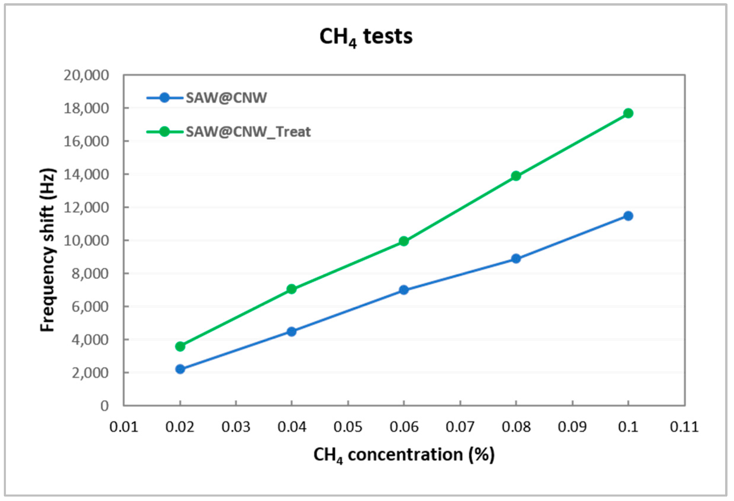
| CH4 (%) | Sensitivity (Δf/c) (Hz/ppm) | LOD (3xn)/(Δf/c) (ppm) | ||
|---|---|---|---|---|
| Before Plasma Treatment | After Plasma Treatment | Before Plasma Treatment | After Plasma Treatment | |
| 0.02 | 11.00 | 18.00 | 6.82 | 4.17 |
| 0.04 | 11.25 | 17.63 | 6.67 | 4.26 |
| 0.06 | 11.67 | 16.58 | 6.43 | 4.52 |
| 0.08 | 11.13 | 17.38 | 6.74 | 4.32 |
| 0.1 | 11.50 | 17.70 | 6.52 | 4.24 |
Disclaimer/Publisher’s Note: The statements, opinions and data contained in all publications are solely those of the individual author(s) and contributor(s) and not of MDPI and/or the editor(s). MDPI and/or the editor(s) disclaim responsibility for any injury to people or property resulting from any ideas, methods, instructions or products referred to in the content. |
© 2023 by the authors. Licensee MDPI, Basel, Switzerland. This article is an open access article distributed under the terms and conditions of the Creative Commons Attribution (CC BY) license (https://creativecommons.org/licenses/by/4.0/).
Share and Cite
Vizireanu, S.; Constantinoiu, I.; Satulu, V.; Stoica, S.D.; Viespe, C. High-Sensitivity H2 and CH4 SAW Sensors with Carbon Nanowalls and Improvement in Their Performance after Plasma Treatment. Chemosensors 2023, 11, 566. https://doi.org/10.3390/chemosensors11110566
Vizireanu S, Constantinoiu I, Satulu V, Stoica SD, Viespe C. High-Sensitivity H2 and CH4 SAW Sensors with Carbon Nanowalls and Improvement in Their Performance after Plasma Treatment. Chemosensors. 2023; 11(11):566. https://doi.org/10.3390/chemosensors11110566
Chicago/Turabian StyleVizireanu, Sorin, Izabela Constantinoiu, Veronica Satulu, Silviu Daniel Stoica, and Cristian Viespe. 2023. "High-Sensitivity H2 and CH4 SAW Sensors with Carbon Nanowalls and Improvement in Their Performance after Plasma Treatment" Chemosensors 11, no. 11: 566. https://doi.org/10.3390/chemosensors11110566
APA StyleVizireanu, S., Constantinoiu, I., Satulu, V., Stoica, S. D., & Viespe, C. (2023). High-Sensitivity H2 and CH4 SAW Sensors with Carbon Nanowalls and Improvement in Their Performance after Plasma Treatment. Chemosensors, 11(11), 566. https://doi.org/10.3390/chemosensors11110566