1. Introduction
Low-power, passive, and non-volatile RF-switches are an area of keen interest among scientists and industry in the current decade. Non-volatile switches would benefit every field of RF-engineering by drastically cutting down the power budget. With the current threshold of development in disposable printed RF electronics, the requirement for passive and low-power switches has intensified.
One of the available solutions for passive, non-volatile switches are Memristive devices such as the conductive bridging random access memory (CBRAM) switches [
1], phase change memory (PCM) switches [
2,
3], etc. These techniques utilize electrochemical properties and molecular arrangement properties of materials, respectively, to achieve the switching action. The CBRAM switch is also referred to as a metal–insulator–metal (MIM) switch owing to its switching layers construction. Working principles and details of this technology are explained in this article. In the case of PCM switches, the change from an amorphous to crystalline state and back of certain materials like germanium telluride upon application of controlled heating pulses are utilized for switching. A handful of articles have reported fine, non-volatile switches based on the above mentioned principles [
1,
2,
4,
5,
6]. However, in the majority of cases, the fabrication technique is very much complicated and often requires a “clean room” facility. Additionally, in most cases the devices are fragile in nature and require dedicated conformal protection schemes to protect it from the ambient atmosphere, and thus adds to the total cost budget.
In this article for the first time we present the design, development, and application of a simple and robust CBRAM based MIM RF-switch on a flexible paper substrate. In this experiment, the entire device fabrication was carried out in ambient laboratory conditions, without the use of any clean room facilities. In this study, we aim to prove the feasibility of integrating a MIM switch in electronically reconfigurable RF devices on flexible and low-cost substrates like paper, which are seen around in our daily life as packaging materials for goods, transport tickets, and visiting cards.
An RF-identification tag using the RF-encoding particle proposed in this paper could be easily fabricated as a sticker, on a paper substrate with an adhesive background, and could be attached to an object, like a barcode sticker, with far more advanced functionalities in comparison to the optical barcodes, like identification out of the optical-line-of-sight, electronic reconfigurability, etc.
2. Motivation and Background
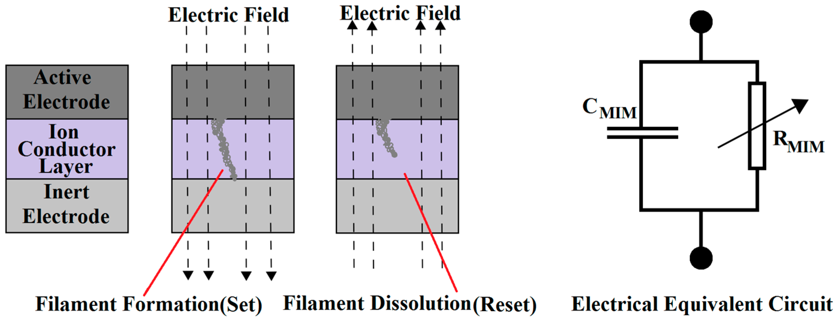
The basic building block of the presented RF-switch is a nano-ionic MIM switching cell.
Figure 1 shows the basic layer structure and working principle of the proposed switching technique. The MIM cell is comparable to a parallel plate capacitor in which the electrolyte is replaced by an ion-conductor, which is an electrically insulating material, such as ‘Poly(methyl methacrylate)’ (PMMA) [
7], doped Chalcogenide glass [
4], Nafion [
8], etc. One electrode of the cell is an ion-donor metal-like silver or copper, generally called the active electrode, and the other is a relatively inert metal like aluminum or gold. On the application of an electric field from active to inert electrode, ions from active electrodes under the influence of this field grow a filament to inert electrode through the ion-conductor layer. This closes the switch, to form the Set state, with a low resistance across the cell. Similarly, a field of opposite direction is used to dissolve the filament and open the switch to form the reset state, with a high resistance across the cell. The switch once commuted to a stable state does not require any maintaining power supply to retain its state, making it a non-volatile passive device. Power is applied to the switch only to change its state. An electrical equivalent model of the MIM switch could be approximated to a parallel plate capacitor in parallel to the filament resistance, as shown in
Figure 1, where C
MIM is equivalent capacitance due to geometry of electrodes and R
MIM is equivalent filament resistance across the cell.
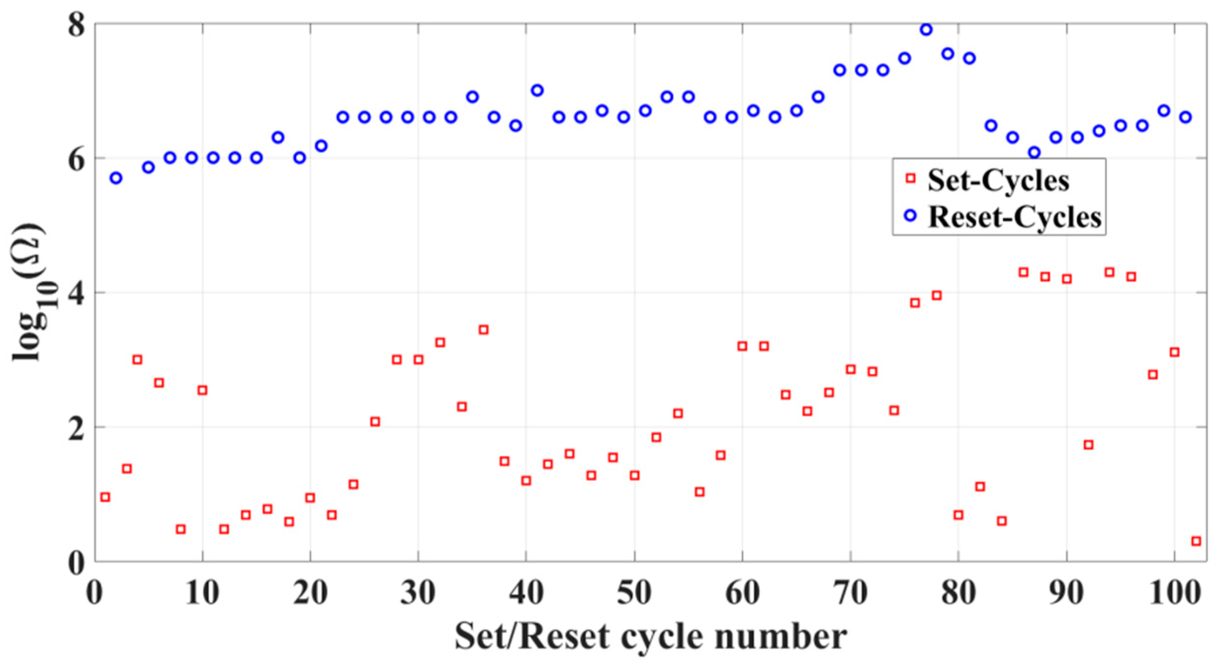
Figure 2 shows 100 switching cycles for a typical MIM cell with Nafion as an ion-conductor v/s filament resistance. We have not yet done a full-fledged study to find out the maximum number of functional cycles or the switching time of the MIM cell, to preserve the devices for detailed RF-characteristics analysis. This will be carried out in near future.
3. Design and Construction
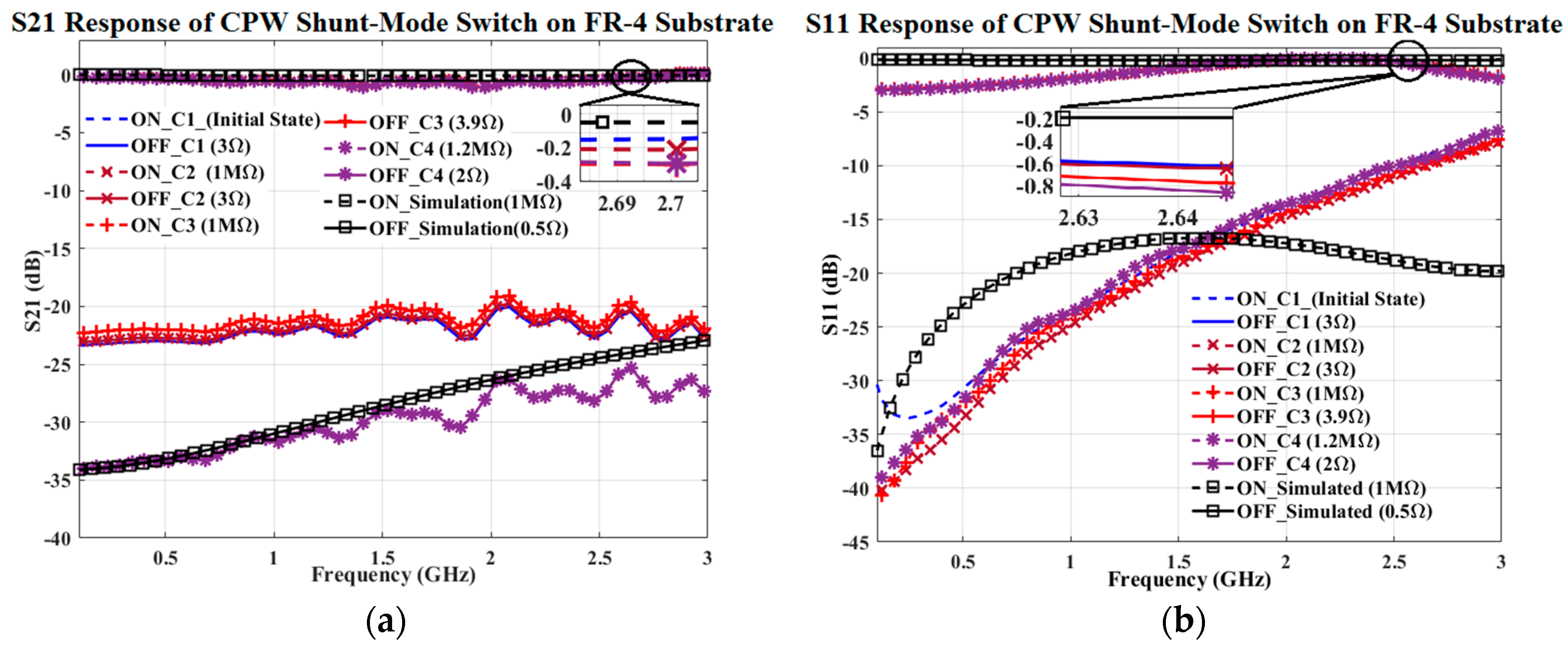
The presented design is a modified version of the predecessor reported in reference [
8]. The reported version in this article [
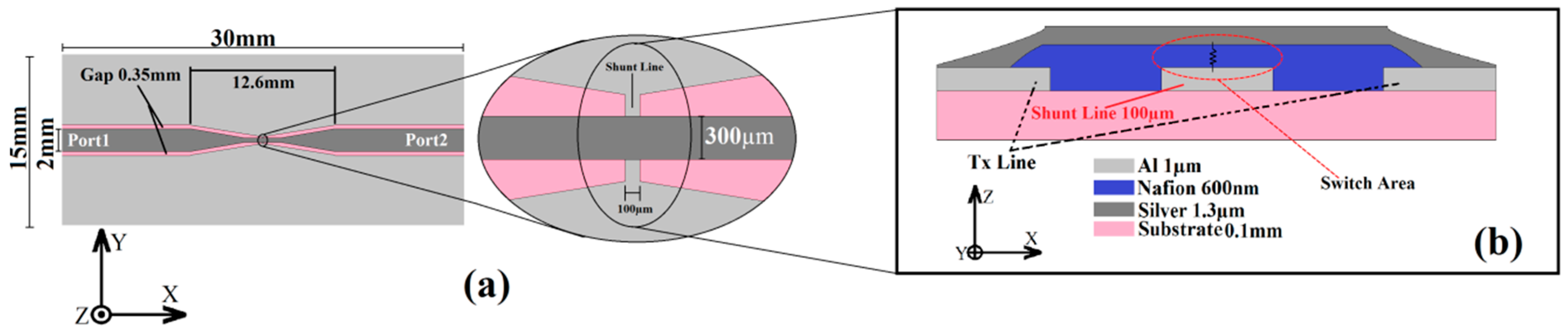
8] is a 50 Ω co-planar waveguide (CPW) transmission line switch in shunt mode on FR-4 substrate, similar to the one shown in
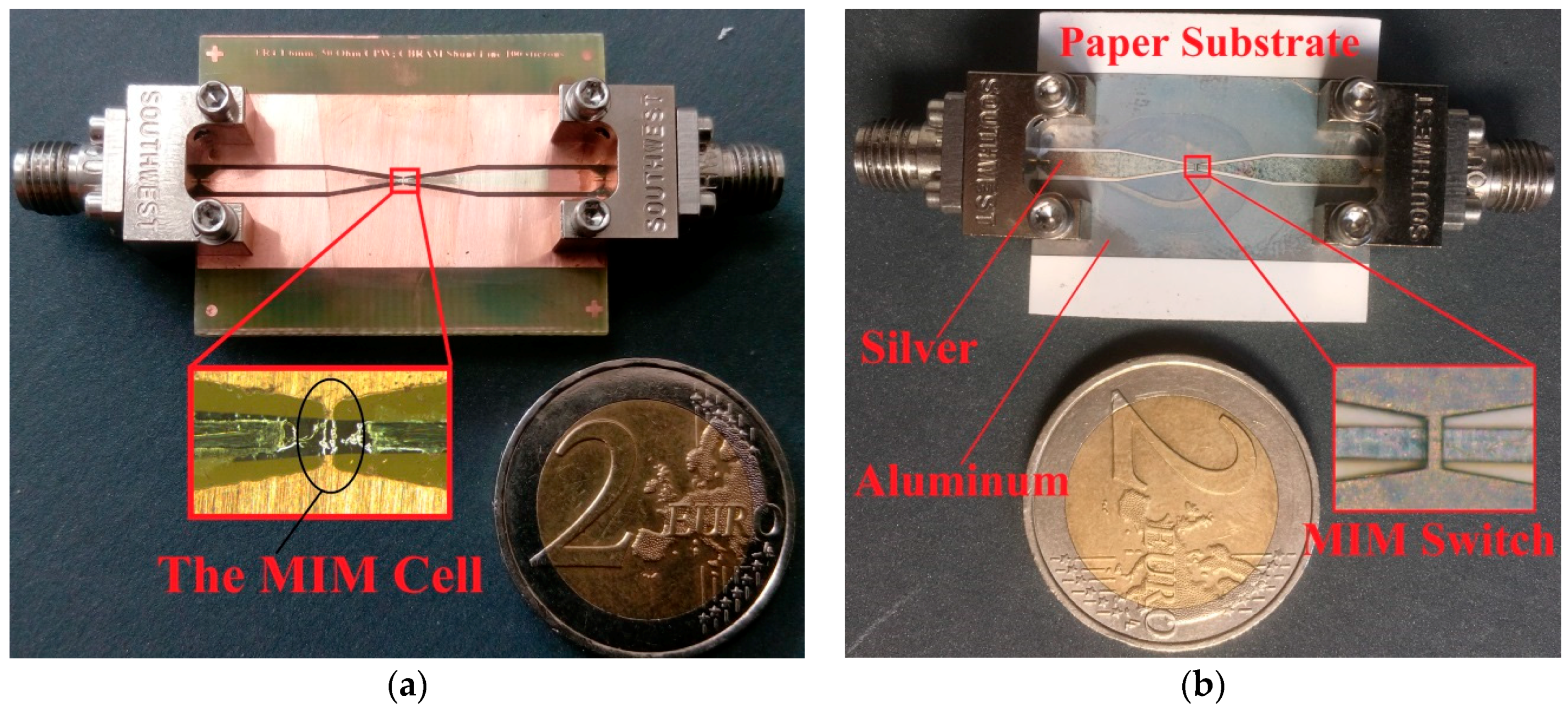
Figure 3. This device is fully fabricated in an ambient environment without the use of any clean room facilities. The device shows good performance features at least up to 3 GHz in comparison with existing switching technologies available. The CPW shunt mode design was chosen over the simple microstrip design to avoid the fabrication difficulties in ambient laboratory conditions. With the microstrip design, there are size limitations on the dimensions of the switching area in order to limit very high capacitance at higher frequencies. This requires having very small dimensions than what is used in this study. The photograph of this realization is depicted in
Figure 4a and the inset shows the close-up microphotograph of the MIM switch area.
In this article we try the same technology on a flexible paper substrate. The topology and dimensions of the switch are given in
Figure 3. The processes used for fabrication are detailed in the following paragraphs.
The substrate used for the fabrication of the device was 80 g per sq. meter (GSM) special quality RF-paper developed at the IES lab. This paper is flexible and specially treated to reduce the losses at radiofrequencies, and also has an improved surface for better adhesion of metal layers. Metal layers were formed on the substrate by thermal vapor deposition of silver (active electrode) and aluminum (inert electrode). Thermal vapor deposition was done with the help of dedicated nickel masks which carry an engraved aperture of the presented topology in
Figure 3. After formation of the active electrode, the electrolyte layer was formed by spin coating the Nafion solution (supplied by Sigma Aldrich, St. Louis, MO, USA) at a rate of 500 RPM for 30 s. The formed layer was then air dried on a hot plate at 100 °C for 2 min. Then the inert electrode was formed using thermal vapor deposition. Detachable SMA connectors are then attached to the device to feed RF power.
It is now apparent that the proposed switch could be integrated into most RF-designs using a three-step process: (1). Deposition of active electrode; (2) Deposition of electrolyte/ion-conductor; (3) Inert electrode deposition. These steps could be easily carried out in an industrial environment by techniques like flexography [
9]. The use of silver metal in the tags could be limited to the switch area only, by adjusting the nickel mask design, so as to reduce further the cost of realization.
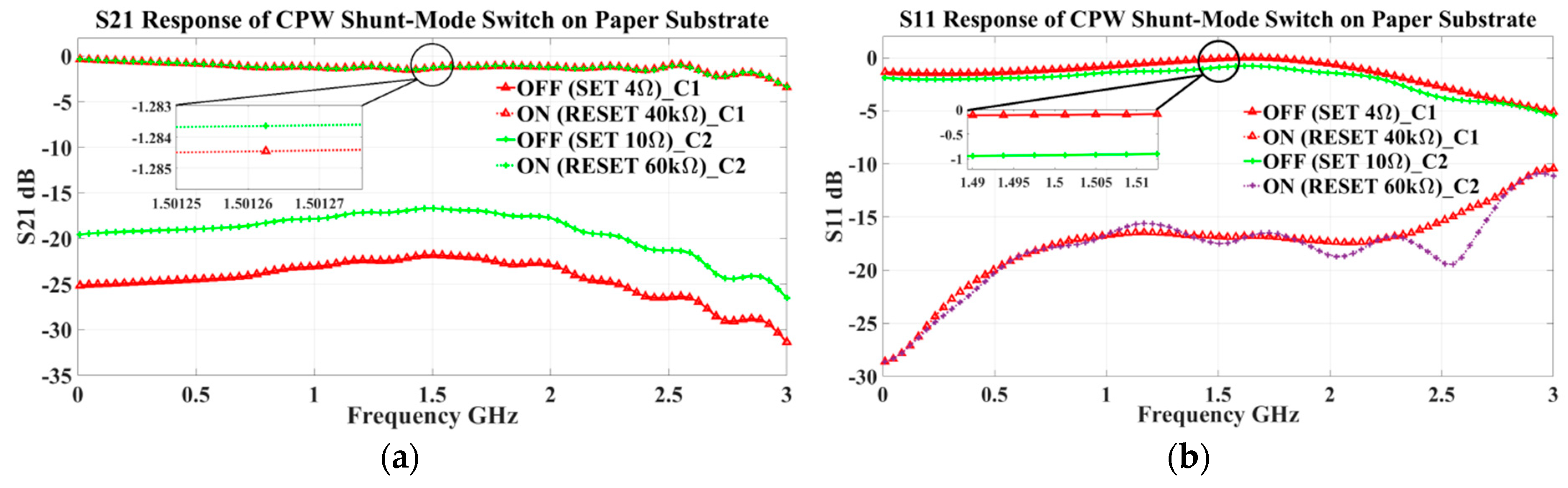
A photograph of the fabricated CPW shunt mode switch on paper substrate is shown in
Figure 4b and the inset shows the microphotograph of MIM switch area revealing the sandwich structure. The thickness of silver and aluminum deposit was measured to be 1.3 µm and 1 µm, respectively, and that of the Nafion deposit is 600 nm. The measurement was carried out with the help of a Dektak-150 mechanical Profilometer.
Nafion [
8] was chosen as the ion-conductor in this realization due to some specific advantages inherent to this polymer in contemplation to materials used classically [
4]. Nafion is a sulfonated tetrafluoroethylene based fluoropolymer-copolymer, well known for its fast ion conducting properties and use in proton-exchange-membrane fuel cells, and is stable up to 190 °C [
10]. Nafion layer could be easily formed by spin coating and could be air dried at temperatures around 100 °C. From our experience in realization, this material is stable in ambient air and does not require an additional conformal coating for protection. The maximum temperature observed on the sample during the thermal vapor deposition was around 120 °C.
The working of the presented CPW shunt mode switch could be explained with reference to
Figure 3. The MIM switch structure is formed in this device between the 100 µm wide shunt line and 300 µm wide transmission line, sandwiching the 600 nm layer of Nafion. The shunt line connectes the two ground planes on the either side of the CPW line. When the MIM switch is set as shown in
Figure 1, at the switch area labeled in
Figure 3b, RF power from port 1 is short circuited to ground, thus disconnecting it from port 2. This is the RF-off state of the switch. When the MIM switch is reset as shown in
Figure 1, the short is removed and port 1 is connected to port 2, forming the RF-on state.
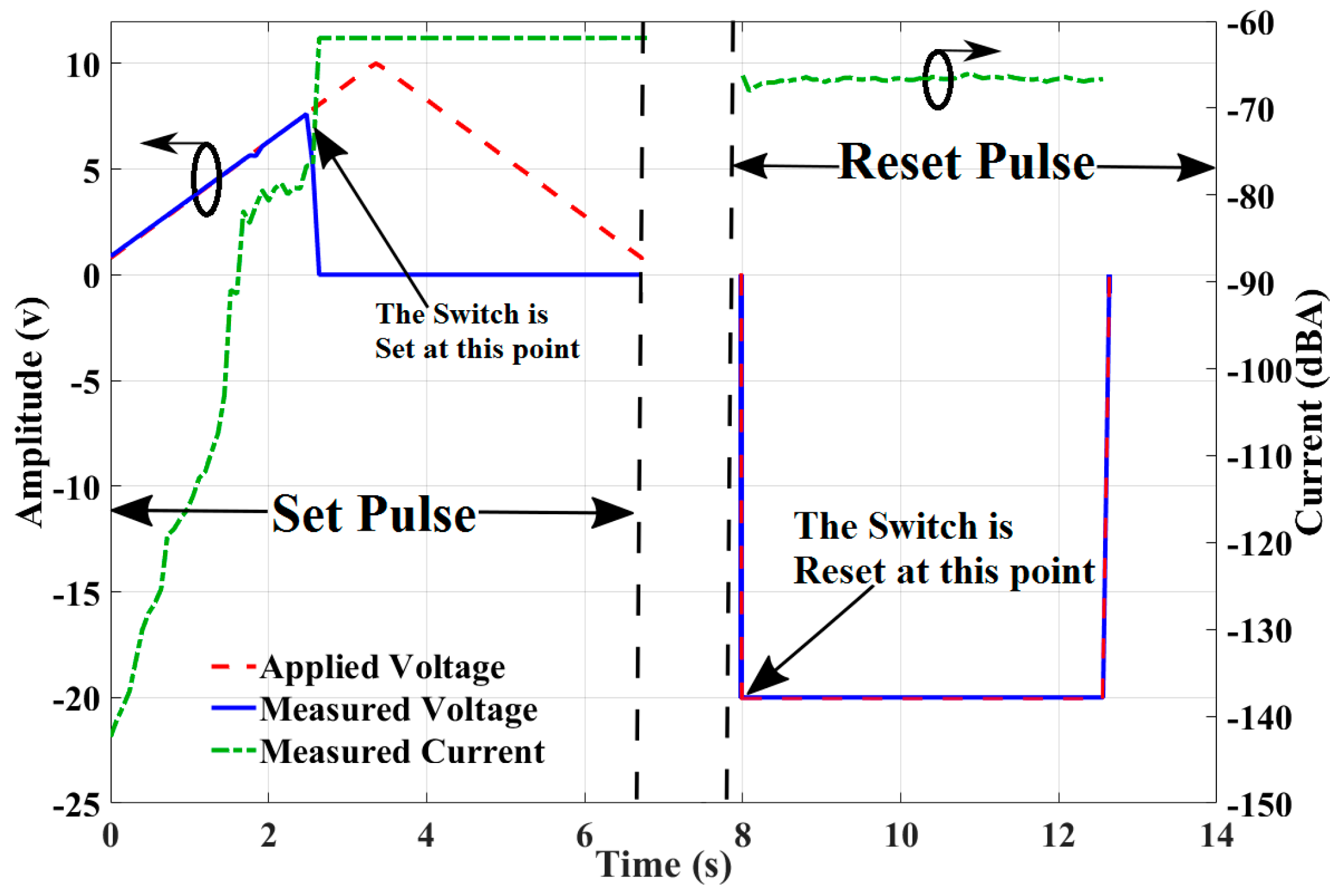
Direct current pulses used for operating the switch are given in
Figure 5. In order to ensure smooth and stable operation of the switch, a positive growing current limited triangular wave form of peak voltage 10 V/0.5 mA is used for the set and a flat −20 V/0.15 A square wave is used for the reset, as shown in the plot. These wave forms were optimized by various trial and error experiments. In the case given in
Figure 5, the switch is set at 7.5 V and reset at −20 V, power consumed for the set and reset are calculated as 0.76 mW and 9.6 mW, respectively. These power values were calculated from the instantaneous value of set/reset voltage and current pulses. An abrupt fall in the measured voltage across the switch and rise in current during the set pulse indicates a set state by the formation of a low resistance filament from active to inert electrode in the MIM Cell (see
Figure 5). Similarly, an abrupt rise in voltage and fall in current during the reset pulse indicates dissolution of filament and establishment of a high-resistance reset state across the MIM cell. The set/reset pulses were applied to the switch with the help of custom made metallic probes attached to metallic parts of the switch.
5. Potential Applications
This idea of fabrication of RF-switches is seen to be functional and feasible in several applications in the field of disposable RF-electronics, in devices such as reconfigurable Radio Frequency Identification (RFID)tags [
11,
12], reconfigurable filters, and reconfigurable antennas.
Radio frequency identification or RFID is a multi-dimensional ingenious concept that has evolved in the past couple of decades and is still advancing at a very high speed. RFID finds application in an all-round domain from identification, sensing, energy, harvesting, etc. [
12,
13,
14].
Amongst this, the chipless-RFID technology is an innovative identification technique often referred to as the “barcode of the future” due to its various versatile functionalities like large read range without optical contact, sensor integration functionality [
11,
14,
15], etc., which cannot be implemented in the current scenario, with the optical barcode technology. Still, a limiting factor to widespread use of this technology is the cost per unit tag in comparison to optical barcodes. However, recent developments in the field of disposable printed RF-electronics would lift this technique to the technology mainstream in near future. Thanks to CBRAM switches for adding revolutionary reconfigurability functionality to the chipless RFID tags, which helps in reducing cost per unit tag and increases the versatility of this technique.
An example of the potential advantage of using the proposed switch technology could be explained as follows.
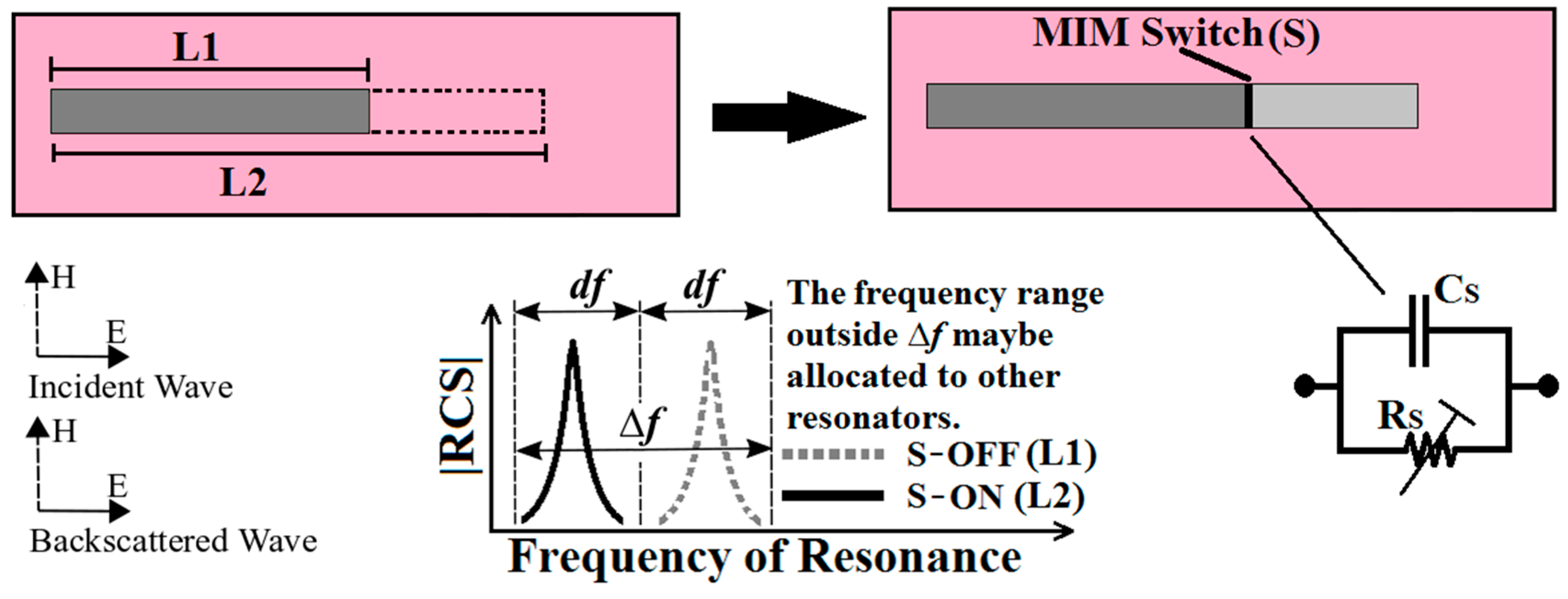
Figure 8 shows the method of frequency shift coding of RF-encoding particles (REP) in a chipless RFID tag [
10,
14]. In this example, a shorted dipole resonator is used as the REP. Classically, this is achieved by modifying the dimensions of each REP on the tag as shown in
Figure 8. For this, a unique geometry has to be designed for each REP. But instead, if we introduce the proposed MIM switch technique to this REP as shown in
Figure 8, the same performance could be achieved with a general REP of fixed dimension, by electronically switching the MIM cell.
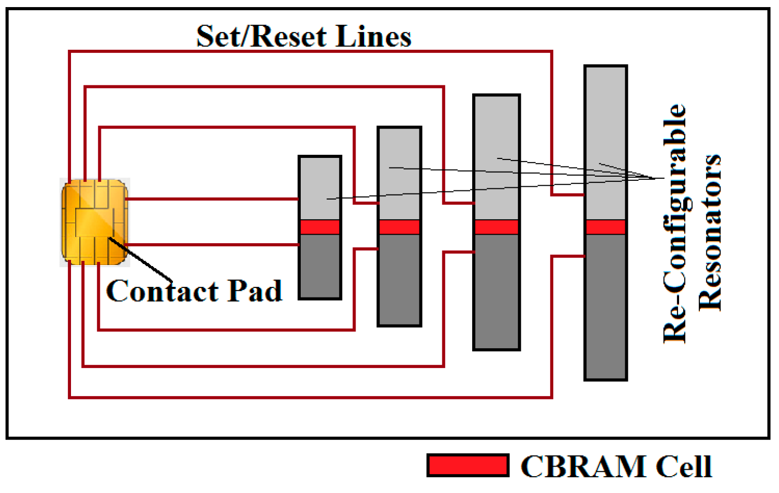
If we integrate such REPs depending on how much bit density is required, on a credit card size tag, with contact pad and set/reset lines, it forms a general reconfigurable chipless RFID card. This could be programmed by a dedicated logic device similar to a credit card reader to encode information. And then could be used for identification in wireless mode similar to a conventional chipless RFID tag. An illustration of this idea is depicted in
Figure 9.
The proof of concept of this technique is reported in Reference [
10], and
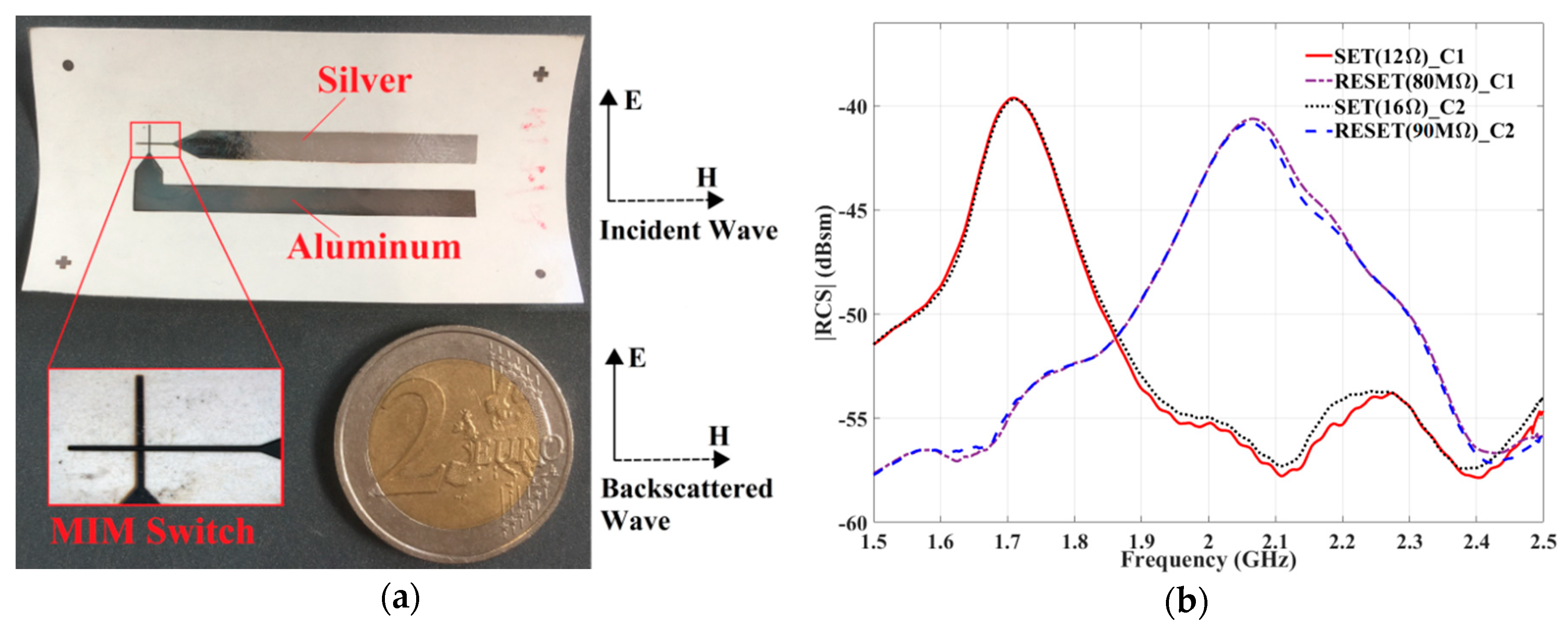
Figure 10a,b shows, respectively, the photograph and response of a similar design on a flexible paper substrate. Fabrication of this tag is carried out in similar way like the RF-switch on paper substrate, by thermal vapor deposition of silver (active) and aluminum (inert) electrodes, and spin coating of Nafion. The proposed design is inspired from the “C” resonator reported in Reference [
16]. Here we use a MIM switch, as shown in
Figure 10a with silver-Nafion-aluminum layers, to reconfigure the resonator by tuning its electrical equivalent circuit depending on the filament resistance (of the nano-ionic filament in the MIM cell). Equivalent circuit analysis and simulation studies of this concept are reported in Reference [
10].
Figure 11 shows the experimental bistatic radar setup using Agilent N5222A PNA and two wide-band horn antennas in co-polarization in an anechoic chamber [
16]. This setup is used to record the RCS response of the tag shown in
Figure 10. It is apparent from these results that we are able to switch the tag at two different resonant frequencies separated by 400 MHz, with set/reset position of the MIM switch.
Discussion on the application of this concept for commercial mass production and use, and the expected convenience is explained in the following paragraphs.
Vena et al. [
17] reports a 20-bit chipless RFID tag. Let us suppose to use this particular tag for labeling applications in which the tag is encoded by using two different dimensions for each resonator. Thus, by using the well-known frequency shift coding technique [
14], Expression (1) could be used to compute the possible number of combinations (refer to
Figure 8 for illustration of the concept of bandwidth allocation for each resonator).
In Expression (1), ∆f is the allocated bandwidth per resonator, df is the bandwidth of resonance of the resonator, k is the number of resonators on the tag, and N is the total number of possible combinations. In this example let us say the allocated bandwidth per resonator is 200 MHz and each resonator resonates with a bandwidth of 100 MHz. So each resonator could be reconfigured by modifying physical size to operate in two different frequencies in the allocated bandwidth. Thus, using Expression (1) we could see that the total number of possible combinations is 1,048,576. Now if we try to fabricate the required combination of tags using classical techniques like screen printing or photolithography, one requires 1,048,576 numbers of masks for the realization of the entire stretch of tags.
The beauty of the proposed concept could be revealed in the following sentences, taking into consideration the amount of labor and number of masks required for the fabrication. If a MIM switch is introduced to each resonator as in Reference [
10] to switch resonators between two different frequencies, then it is apparent from the presented work that the switch/tag could be fabricated using just two masks and spin coating of Nafion. Similarly, for this particular RFID tag, the entire stretch of tags could be fabricated as a general tag using just two masks. Then, a dedicated electronic pulse programming circuit with an electrode array could be used to set/reset the respective switches and to encode each tag. In essence, the complexity of requirement of the 1,048,576 unique masks for fabrication is solved by just using two masks and a dedicated programmer circuit. This example clearly indicates the leverage of application of this technology in reconfigurable chipless RFID tags.

 ,
, 


