Abstract
Mu3e is a dedicated experiment designed to find or exclude the charged lepton flavor violating eee decay at branching fractions above . The search is pursued in two operational phases: Phase I uses an existing beamline at the Paul Scherrer Institute (PSI), targeting a single event sensitivity of , while the ultimate sensitivity is reached in Phase II using a high intensity muon beamline under study at PSI. As the eee decay is heavily suppressed in the Standard Model of particle physics, the observation of such a signal would be an unambiguous indication of the existence of new physics. Achieving the desired sensitivity requires a high rate of muons ( stopped muons per second) along with a detector with large kinematic acceptance and efficiency, able to reconstruct the low momentum of the decay electrons and positrons. To achieve this goal, the Mu3e experiment is mounted with an ultra thin tracking detector based on monolithic active pixel sensors for excellent momentum and vertex resolution, combined with scintillating fibers and tiles for precise timing measurements.
1. Introduction
1.1. Motivation
Mu3e [1] is a dedicated experiment designed to search for the rare charged lepton flavor violating (cLFV) decay μ+ → e+e−e+. In the Standard Model of particle physics this decay is forbidden at tree level and can only occur via neutrino mixing through higher order loop diagrams, as depicted in Figure 1a. These processes are heavily suppressed, with branching ratios [2], and their observation is unfeasible with the current experimental techniques. Hence, the observation of such an event would be a clear indication of the presence of physics beyond the Standard Model, possibly mediated by the exchange of very heavy particles. Such particles could have masses of TeV and would not be visible in direct measurements at the Large Hadron Collider at CERN (Switzerland), but are expected in many theoretical models, such as supersymmetry (SUSY), models with extra Higgs bosons or models with extra dimensions. The muon decay into three electrons via slepton mixing as described in SUSY models is shown in Figure 1b for illustration.

Figure 1.
Feynman diagram of the decay of the muon into three electrons (a) via neutrino mixing in the Standard Model and (b) via slepton mixing in the SUSY model.
The Mu3e experiment is under construction at the Paul Scherrer Institute (PSI) in Villigen (Switzerland). The ultimate goal of the experiment is to observe the μ+ → e+e−e+ process assuming its branching fraction is larger than , or in case of a negative result to exclude a branching fraction larger than at 90% confidence level. PSI has been at the forefront of cLFV searches for decades, owing to its high intensity muon beam lines. The Mu3e experiment is unique in addressing the μ+ → e+e−e+ decay process: its sensitivity is expected to improve on the latest measurements of the μ+ → e+e−e+ branching fraction by the SINDRUM experiment [3] by almost three orders of magnitude. Mu3e complements various worldwide high priority programs searching for other muon decays, such as MEG-II [4] at PSI, expected to reach a sensitivity to the e decay of , and Mu2e [5] at Fermilab (US) and COMET [6] at J-Parc (Japan), both expected to reach sensitivities to the neutrinoless e conversion of .
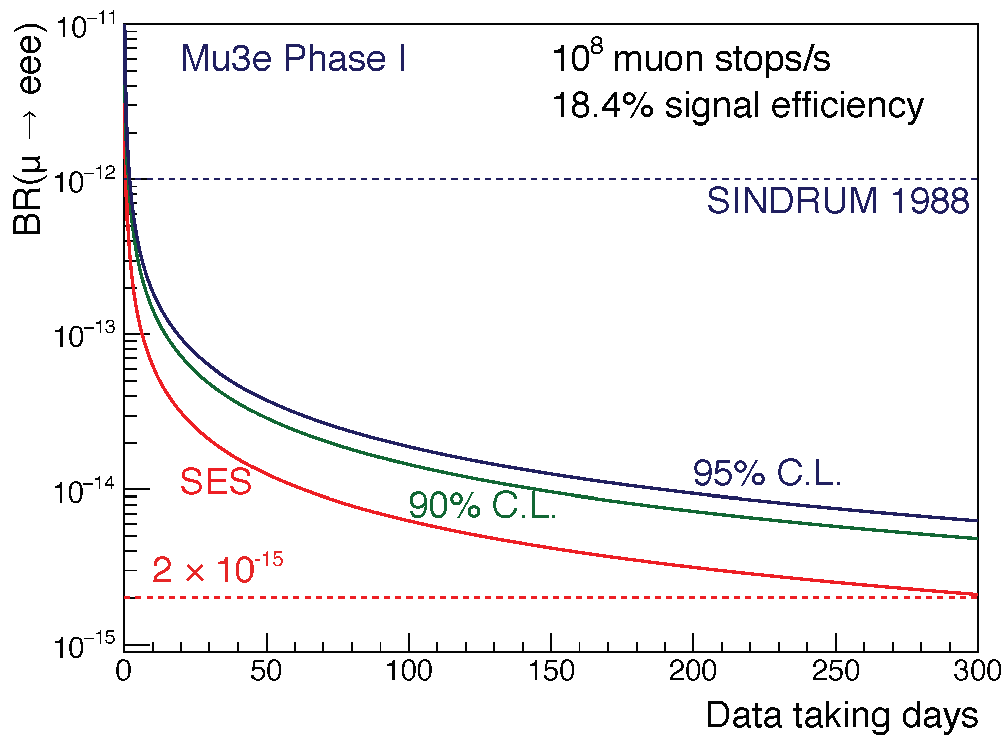
Mu3e is realized in a two-stage approach: the first experimental phase (Phase I) uses the existing beamline at PSI, the world’s most intense muon beam, which provides up to stopped muons on target per second. These muons come from stopped pions decaying at rest close to the surface of the production target. As negative pions are immediately absorbed in the target and do not decay into muons, it results in a very intense and pure positive muon beam. Phase I is foreseen to start physics operations in 2024 and it is designed to reach a single event sensitivity (SES) on the branching fraction of after a running time of around 290 days, as shown in Figure 2. The second phase (Phase II) aims for a single event sensitivity. It requires a novel beamline, the High intensity Muon Beamline (HiMB) [1,7], capable of delivering muons on target per second, which is planned to be available at PSI starting 2028.
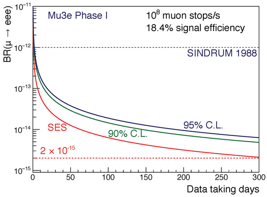
Figure 2.
Single event sensitivity (SES) and corresponding 90% and 95% C.L. upper limits versus data taking days for the Phase I Mu3e detector [1].
1.2. Signal and Backgrounds
The μ+ → e+e−e+ process features a prominent event topology of three particles of identical mass, the two positrons and one electron, which leave a clear signature in the experimental apparatus. The Mu3e detector is designed to optimally track the two positrons and the one electron from muons decaying at rest and to fully reconstruct the event kinematics. Energy and momentum conservation are exploited to discriminate the μ+ → e+e−e+ signal from the backgrounds. In the experiment, the muons stop on a thin target before decaying, thus the sum of the momenta of the three decay electrons vanishes, meaning
At the same time, the total energy of the products sums up the muon rest mass,
The energies of the decay particles range from the electron mass up to half the muon mass (∼53 MeV). The decay is assumed to be prompt, hence all products are created from a common vertex in space and in timing coincidence.
The dynamics of the decay are dependent on the underlying nature of the unknown charged lepton flavor violating mechanism. Such effects are parametrized in the Lagrangian proposed by Kuno and Okada [8], which encodes different signal models according to their coupling type (dipole, scalar or vector-like). More details on the modelling of the signal can be found in [1]. Targeting a three-body decay with unknown kinematics, the acceptance of the Mu3e detector must be maximized o have the maximum possible phase space coverage. This is achieved with a large solid angle coverage and a track reconstruction of particles with momenta as low as a few MeV.
The experimental reach of Mu3e likewise depends on the ability to suppress the main sources of background contamination below the target sensitivity. Two types of backgrounds are present in the experiment: the internal conversion background, which is irreducible and mimics the signature of the μ+ → e+e−e+ decay, and the accidental background, which is combinatorial.
The irreducible background arises from muon radiative decays with internal conversion ( eee): the positron from a Michel decay ( e) radiates a virtual photon that creates an additional electron-positron pair. The process is a very interesting decay mode by itself, as it can be used to scrutinise the Standard Model, and is well suited to calibrate the detector. It occurs with a branching fraction of and in this case the neutrinos typically carry away only a very small energy fraction. This means that the only way to identify this background is with high momentum and energy resolutions to infer the presence of the undetected neutrinos; hence, the momentum resolution of the experiment directly determines at what level it can be suppressed. To ensure the sensitivity expected for Phase I, the average three-particle mass resolution has to be better than 1 MeV, which drives the experimental design described in Section 2.
The second type of background is accidental (also called combinatorial) and results from overlays of different processes producing three tracks that resemble the signal decay. With a branching fraction close to 100%, Michel decays ( e) are the main sources of positrons. The additional electron typically emerges from Bhabha scattering or radiative muon decays. Inefficiencies in the track reconstruction, misidentification of the charge and the presence of fake tracks additionally contribute to the accidental background. The capability of discriminating the vertices from different muon decays is a key tool to suppress the combinatorial background. Additionally, at high muon rates, excellent time resolution is essential to suppress the accidental background and to facilitate the global event reconstruction.
2. Phase I Experimental Concept
This paper is intended to be a description of Mu3e design and the results obtained from the different subsystem R&D campaigns. Most of this information can be found in the Technical Design Review (TDR) [1].
Mu3e is a stopping target experiment located at the E5 channel of Compact Muon Beam Line at PSI, which delivers the so-called surface muons, i.e., muons produced from stopped pions decaying at the surface of a primary production target. After the positron contamination is removed, a beam of up to 10 muons () per second is transported to the center of the Mu3e experiment. The beam is stopped on a hollow double-cone target, which spreads out the decay vertices in the longitudinal direction and minimizes the material budget traversed by the decay particles. The target is made of Mylar and is designed to have a high stopping power; it is thick in the front part and thick in the back part, with a total length of 100 mm and a radius of 19 mm.
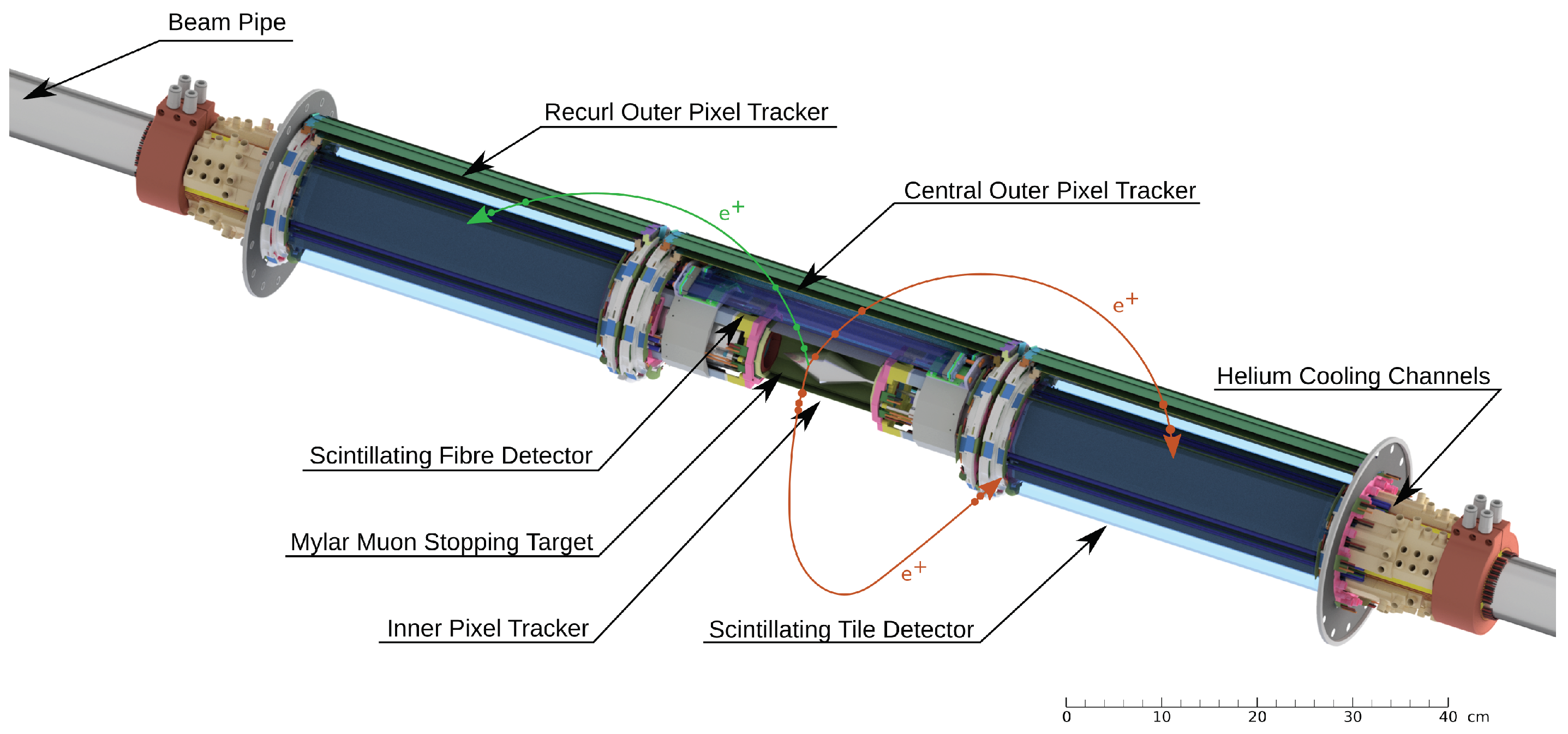
The target is surrounded by a series of sub-detectors, shown in Figure 3. The sensitivity goal of the Mu3e experiment poses strict requirements on the design of such subsystems. To search for the rare μ+ → e+e−e+ events within a reasonable running time, besides the extremely high muon rate, an excellent momentum vector, vertex and timing resolution is required. Precise momentum and vertex resolution are obtained with a light-weight silicon pixel tracker in the central and outer regions (see Section 3) placed inside a 1 Tesla solenoidal magnetic field. It is complemented with two timing detectors (see Section 4) in the central and outer regions, respectively, for a precision requirement on the simultaneity of the three particle tracks arising from the target.
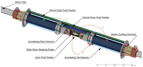
Figure 3.
Active part of the Mu3e detector, with a central tracker surrounding the target, and the upstream and downstream tracking stations. The large lever arm created by the recurling tracks grants the required momentum resolution [1].
To measure the decay electron momenta, the entire detector is mounted in the bore of a 3-meter long superconducting magnet. A solenoidal magnetic field of 1 Tesla has been identified as the best compromise between beam area space constraints, detector compactness and field homogeneity [1]. The last one in particular is very important for precise momentum measurements: the field inhomogeneity must be lower than 10 within ±60 cm from the target to achieve the desired resolution. Given the complexity of such a device, its design and construction has been outsourced to the company Cryogenic Ltd. The magnet has been fully commissioned and is operational.
Given the low energy regime (below ∼50 MeV) and the very high magnetic field, the electrons/positrons recurl back following a helical trajectory, also known as a recurling track, either crossing the central tracker again or hitting the outer tracking stations, as shown in Figure 4. At these energies, the Coulomb scattering in the detector material is the main contribution to the degradation of the momentum resolution. The detector design, therefore, is conceived to minimize multiple scattering effects on the recurling tracks. This can be achieved with a long narrow tube, where the radius is optimised to the chosen magnetic field [1].

Figure 4.
Schematic view of the Mu3e detector in the longitudinal and transverse planes, showing the recurling tracks of two positrons (in red) and one electron (in blue) issued from a muon decay on target [1].
Multiple scattering is also mitigated by reducing the material budget of the whole detector. Several strategies have been implemented to this end. For instance, the pixel sensors are based on High Voltage Complementary Metal–Oxide–Semiconductor (HV-CMOS) technology [9], which allows for ultra-thin sensors with high performance, while the tracker cooling system is based on gaseous helium. Vertex reconstruction is also prerogative of the pixel tracker, in particular the two innermost layers. The resolution, in this case, depends mainly on geometrical factors, such as sensor position and pixel size. With the foreseen design of the tracker, a vertex resolution of about 0.5 mm can be achieved.
At the high muon rates expected at the Mu3e experiment, precise timing of the tracks is essential for event building and to suppress the combinatorial background. In order to reduce this background by at least two orders of magnitude, the timing resolution should be below 500 ps to allow for reliable track identification, and ideally below 100 ps to resolve non-synchronous muon decays. To this end, the silicon detector layers are complemented by two timing systems, consisting of a scintillating fiber tracker in the central part of the experiment (see Section 4.1) and scintillating tiles inside the recurl layers (see Section 4.2). In addition to the timing, the detectors help to resolve the curvature sign, i.e., the charge, of the recurling tracks by the time of flight measurements and to reject mis-reconstructed tracks with confused recurling track segments.
The fiber detector has a cylindrical shape and is installed around the pixel tracker’s innermost layers to allow for an easy association between a track and its timestamp. The fibers must have a time resolution of few hundreds of picoseconds, a spatial resolution of 100 μm and a thickness of X/X< 0.2%. The tile detector, instead, is installed in the two recurl stations of Mu3e, and hence it is not subject to requirements on the detector material thickness. In this case, a time resolution of less than 100 ps is helpful to further reduce the combinatorial background. Given the low density of tracks in this region, space resolution can be as large as few millimeters. For a correct association between tracks and timing detector hits, the pixel sensors must have a good timing resolution as well, and therefore it is required to be less than 20 ns.
The aforementioned requirements on the Mu3e performance lead to the subdetector designs described in the following sections. As of late 2021, all Mu3e detector subsystems are under construction; a more detailed scheduled on the installation and construction is provided in Section 6.
3. Pixel Tracker
3.1. Phase I Layout
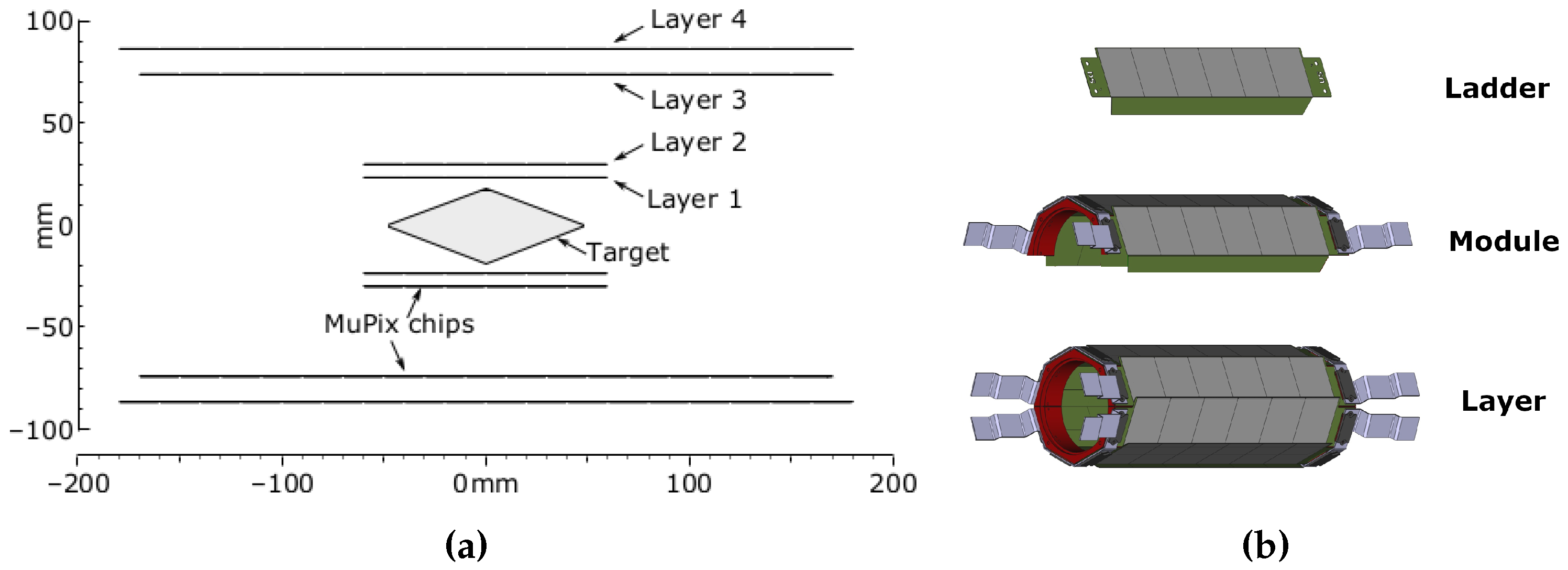
In the Mu3e experiment, the pixel tracker is the system responsible for identifying vertices and measuring the momenta of the decay electrons. It consists of 2844 pixel sensors arranged in three stations: one central, one upstream and one downstream. The lateral layout of the tracker’s central station can be found in Figure 5a. The geometry of the three stations is based on coaxial cylinders, called layers. In each layer the pixel sensors are placed in line on mechanical units called ladders. The ladders are then arranged circularly around the cylinder axis to form the layers. The central station comprises four layers, which are divided in two by timing detectors: 2 inner layers (1 and 2) and two outer layers (3 and 4). The recurl stations consist of outer layers only.

Figure 5.
(a) Lateral layout of the tracker’s central station. (b) CAD drawing of the Mu3e tracker’s mechanical components. The violet stripes are parts of the electrical connections, which are integrated in the module mechanics [1].
From the mechanical point of view, the ladders are grouped in modules, which are then assembled together to form the layers (see Figure 5b). The modules are more robust units than the single ladders, so that they can be individually mounted onto the end-rings, the support structures that hold the layers around the beamline. The geometry of the modules and ladders varies for each layer, and is summarized in Table 1.

Table 1.
Pixel tracker geometry parameters of the central barrel. The radius is defined as the nearest distance of sensor w/o polyimide support to the symmetry axis (beam line). From [1].
The chip active area consists of 250 × 256 pixels, each one 80 × 80 μ2 large. Given that each pixel sensor has an active area of about 2 × 2 cm2, the total active area of the pixel tracker is 11,376 cm2.
3.2. Pixel Sensor
As anticipated in Section 2, the sensors for the Mu3e pixel tracker are based on the HV-CMOS technology. The sensors developed specifically for the Mu3e experiment are High Voltage Monlithic Active Pixel Sensors (HV-MAPS) called the MuPix sensors, which are produced in commercial 180 nm technology. Being at the forefront of HV-CMOS R&D, Mu3e has gradually implemented the experimental requirements at each stage of the MUPIX development. In spring 2020 MuPix10 [10] was produced. It implements all the required features, including a fully monolithic read-out and a full size active area.
The choice of the HV-MAPS over hybrid sensors, more common in HEP, was driven by material budget considerations. Being fully monolithic CMOS, these sensors do not require front-end chips to be read. Therefore, with a thinning procedure, the total silicon thickness per layer can be reduced down to 50 μm. To improve the performance of the standard CMOS technology, the read-out electronics of each pixel is embedded inside a deep n-well, which sits in the p-substrate. This way, a high negative bias voltage can be applied without compromising the electronics, hence the name HV-MAPS. The high bias voltage increases the depletion region and the electric field, which improves the signal size and the charge collection speed. These features are necessary to meet the Mu3e experimental requirements for the pixel sensors, i.e., an efficiency higher than 99.5% and a time resolution of less than 20 ns.
The in-pixel analogue read-out is similar for all the MuPix sensor prototypes, and it is made of a sensor diode, a charge-sensitive amplifier and a source follower to drive the signal to the chip periphery. Every pixel cell is mirrored by a digital buffer cell in the periphery, which receives the pixel signal and digitizes it. In this process the analogue signal is compared against a threshold, and rising edge and falling edge are sampled with a 8 ns clock. From the difference of the two timestamps, the Time-over-Threshold can be computed. The latest MuPix prototypes implement a second threshold, which can be used for more precise time measurements. A state machine reads the buffers from the digital pixel cells and sends out the hit data.
3.3. Detector Integration
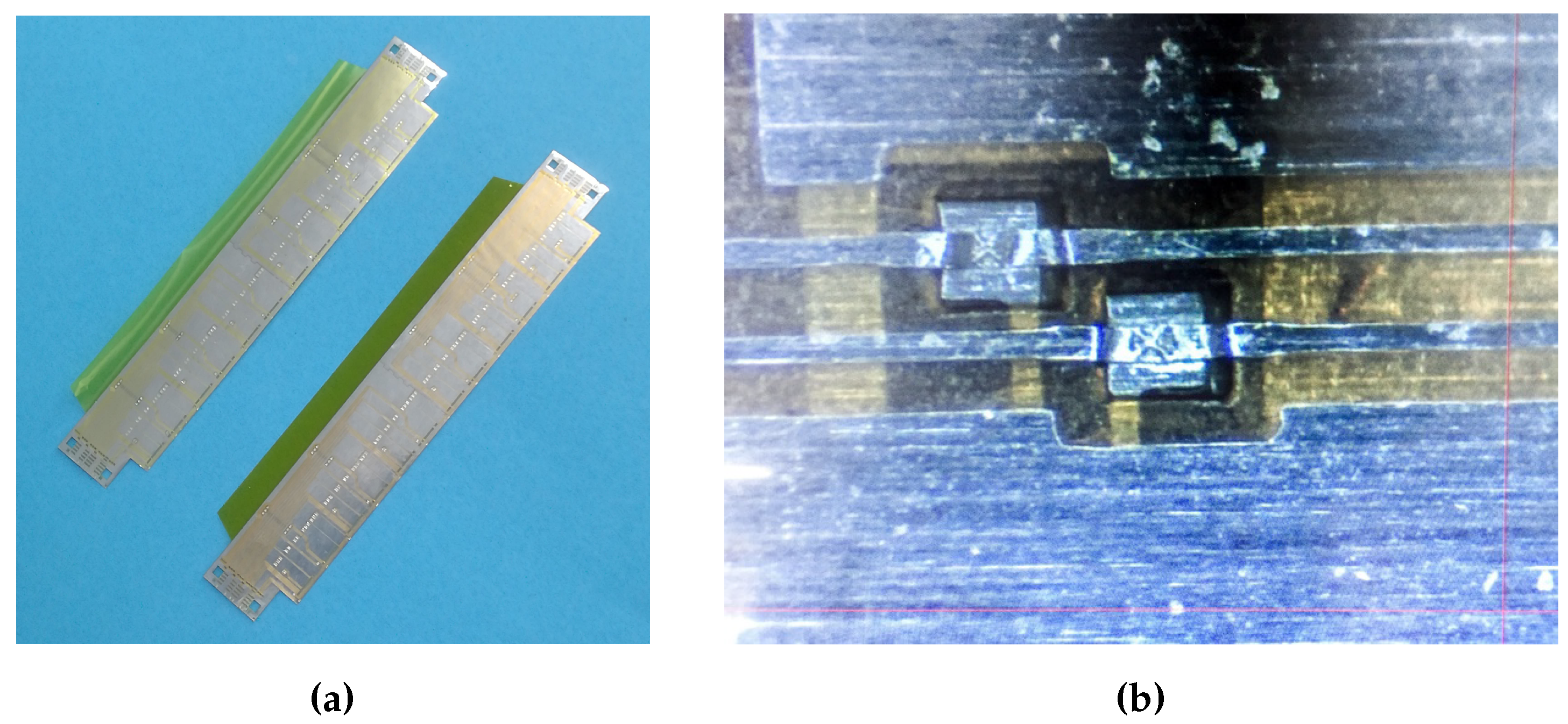
The mechanical and electrical integration strategy is also driven by material budget considerations: the thickness of the components is minimized and low-Z materials are used wherever possible. The ladders, which are the smallest mechanical units, are based on High Density Interconnect (HDI) circuits. These are produced by LTU [11], and are composed of thin polyimide foils intervealed with aluminum traces (see Figure 6a). The latter provide power and high voltage, as well as transmitting the signals to the chips and the data outwards, such that no more components are needed on the flex-prints. The MuPix chips are then glued to the HDIs and connected to the aluminum traces via Single-point Tape Automated Bonding (SpTAB). This technique allows for direct bonding of the traces to the on-chip bond pads without the addition of extra material (see Figure 6b). A breakdown of the material budget per layer is shown in Table 2. Thanks to all these features, the total radiation length can be reduced to approximately per layer. Simulations of the tracker performance show that, with this geometry and material budget, its momentum resolution is lower than 1.5 MeV [1].
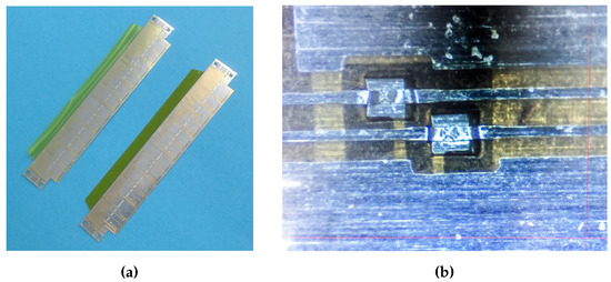
Figure 6.
(a) Picture of a HDI flex for the tracker inner layers. (b) Microscope picture of a HDI aluminum trace spTA-bonded to a test pad. Courtesy of LTU [1].

Table 2.
Material budget of a MuPix ladder. The thicknesses and radiation length are given as an average over the mm width of the ladder. From [1].
On the outer edges of the HDI circuits, the aluminum traces are connected via spTAB to a flex-print circuit called the interposer flex. The interposer flex is then connected to another flex-print circuit, the endpiece flex, by means of industrially-produced interposers. These provide micro-grid arrays of gold-spring contacts and are fixed together with the flex-prints by mounting brackets and screws. The endpiece flex further extends the signal and power lines around the end-rings towards a dedicated PCB. From there, the signal lines are routed to the DAQ readout boards (see Section 5.1) through micro-twisted pair cables of diameter. From the same PCB, the power lines are connected to the copper rods around the beampipe (see Section 5.2.2).
3.4. Cooling System
The material budget minimization is the main factor in the choice of the cooling system as well, and it lead to the employment of a gaseous helium system. The purpose of the cooling system is to keep the detector below 70 degrees Celsius in any point, since that is the glass-transition temperature of the adhesives used for construction. In a conservative scenario, the power consumption of the pixel sensors is 400 mW/cm, for a total power dissipation of 4.55 kW. From the studies of MuPix10, a total power consumption of 2.844 kW can be assumed for a realistic scenario.
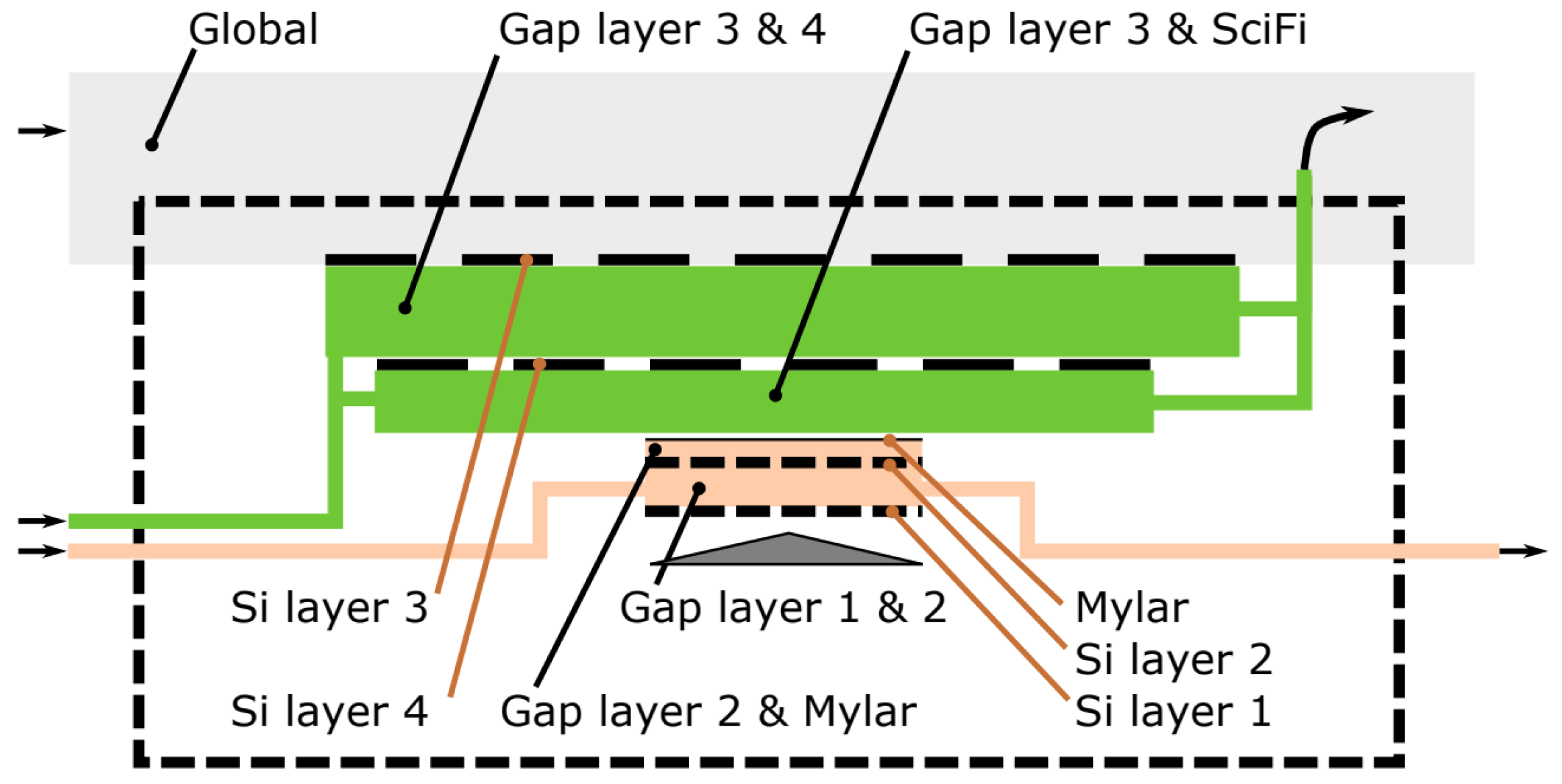
The helium is introduced in the system at a temperature of about 0 Celsius and pressure of 1 bar. The gaseous flow is then directed in different channels, as in Figure 7. A thin mylar cylinder surrounds the pixel detector to ensure constant helium velocity.

Figure 7.
Sketch of the helium cooling system for the pixel tracker central station (the area inside the dashed box) showing the inner layer flow (pink), the outer layer flow (green) and an additional global flow inside the magnet (gray) [12].
The design of the cooling system was based on detailed simulations, which show that the maximum temperature difference between the helium inlet and any point in the tracker is 62 degrees Celsius [1].
3.5. Prototyping and Tests
Several R&D projects have been performed to prove the basic concepts and solutions adopted for the Mu3e tracking system. The main subjects of research were the MuPix development and the thermo-mechanical prototype.
3.5.1. MuPix Performance
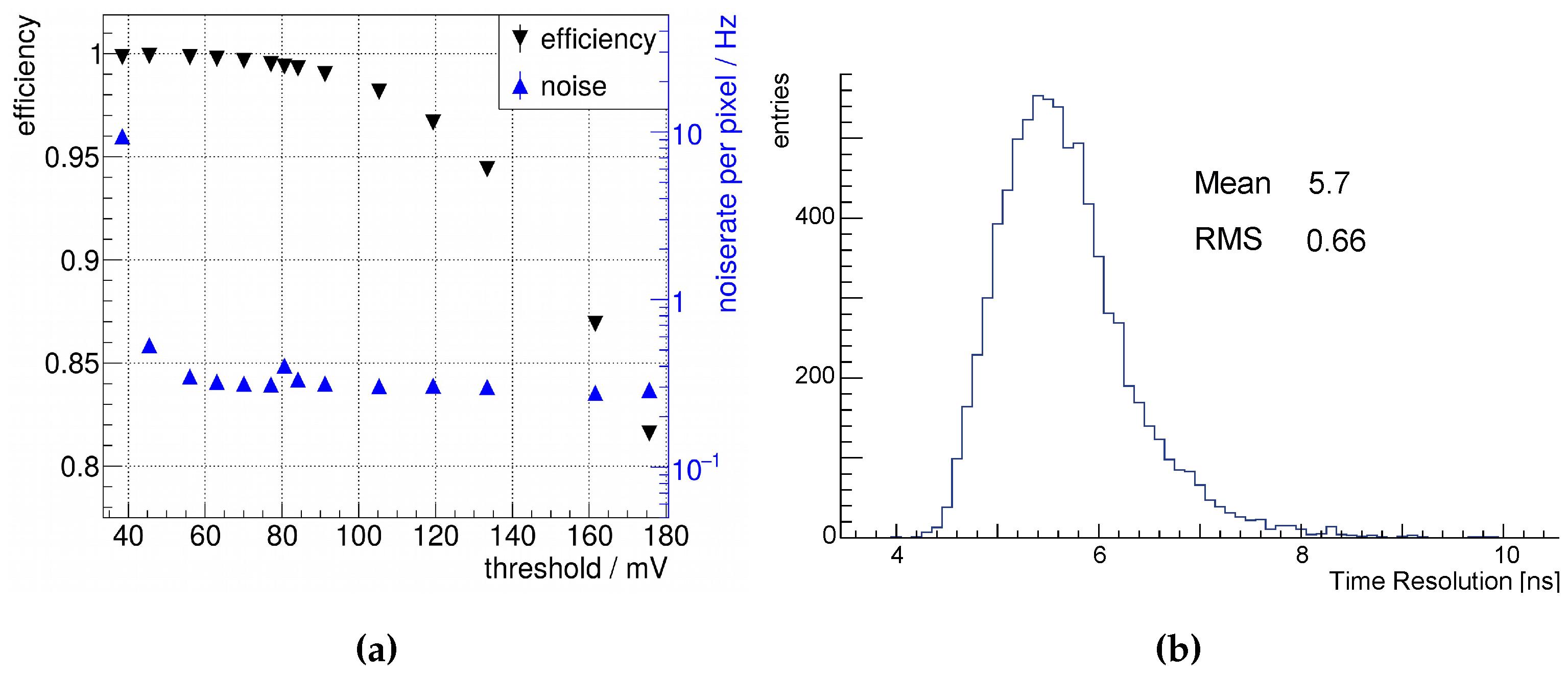
The efficiency and time resolution of MuPix sensors have been investigated in several test beam campaigns at DESY and PSI with electrons and pions respectively. There, the prototypes have been exposed to a high energy particle beam, while the particle tracks have been reconstructed with a pixel telescope. By matching the telescope tracks with the prototype’s hit, the efficiency can be calculated for every pixel. At the same time, the pixel noise can be extrapolated from hits that are not associated with any track (see Figure 8a). These results show that the sensors meet the Mu3e efficiency and noise requirements in a threshold range of about 40–90 mV, corresponding to about 650–1450 electrons.
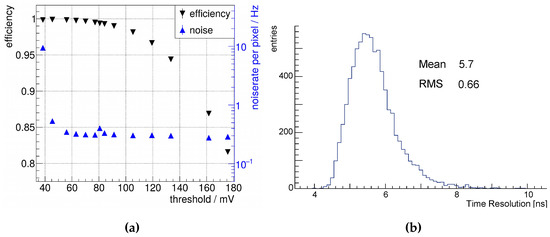
Figure 8.
(a) Efficiency and noise vs. threshold for a MuPix8 chip obtained in test beam. (b) Distribution of the measured MuPix8 time resolutions of individual pixels obtained with the 2-comparator threshold method and after time-walk correction using a 90Sr source [1].
The time resolution was studied in test beam or with a Sr source by using a scintillator as time reference. The overall time resolution in MuPix sensors is worsened by mainly two factors: hit delay and time-walk. The first is due to the time for the analogue signal generated in the pixel to reach the digital cell in the periphery, and it depends on the pixel position in the matrix. The time-walk is due to the fact that higher signals have higher rise-time, and it therefore depends on the signal amplitude, which is related to the Time-over-Threshold (ToT). By investigating these dependencies, the time of arrival (rising edge) of each hit can be corrected and the resulting time resolution with the two-threshold sampling method is 5.7 ns (Figure 8b), well within the experimental requirements.
3.5.2. Thermo-Mechanical Mockup
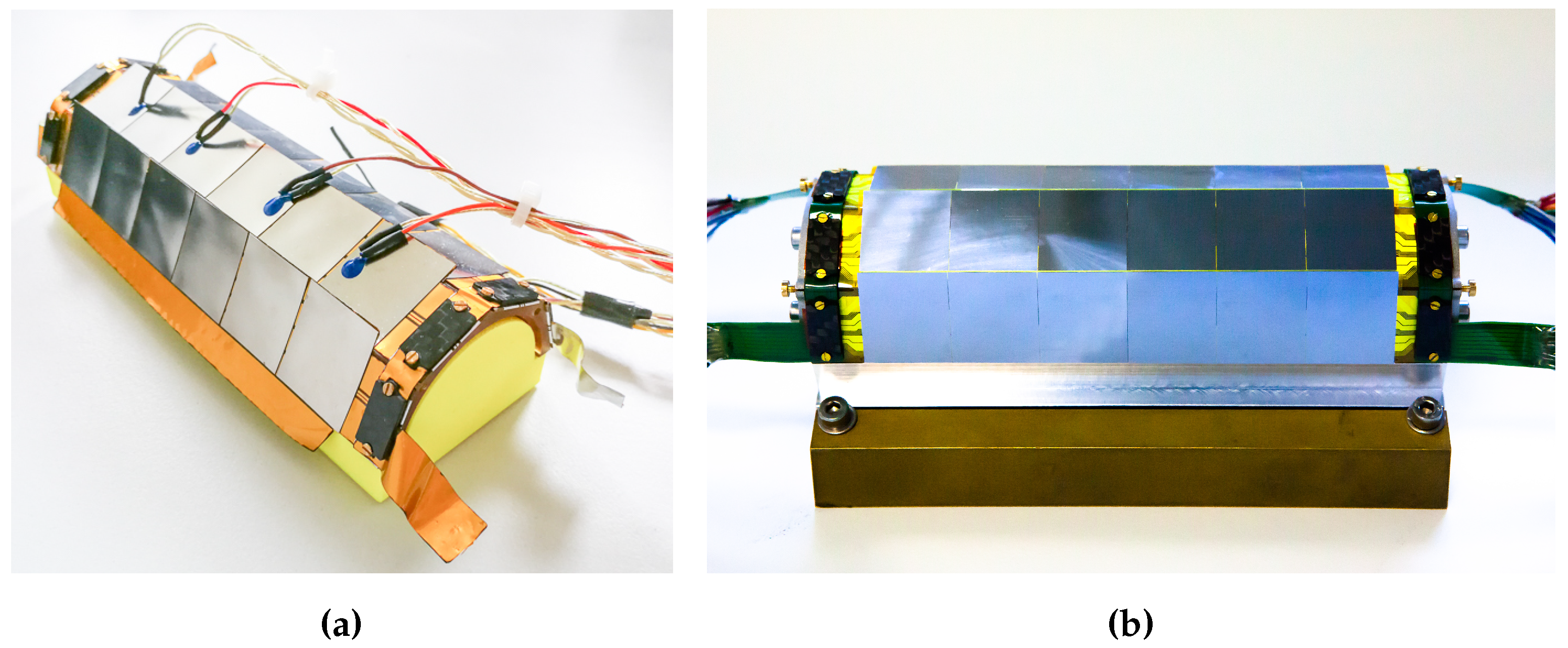
Another key study to prove the feasibility of the Mu3e tracker concept has been performed with thermo-mechanical mockup prototypes. This is a reproduction of the tracker itself made with passive components and temperature monitor circuitry. The aim is to match the material and power consumption of the final detector, to prove its mechanical stability and the performance of the cooling system. Two series of prototypes have been produced: the tape heater ladders and the silicon heater ladders. The first are made of thick stainless steel dummy chips attached to aluminium-polyimide laminate resistive heating circuits (see Figure 9a). The circuits are laser-cut and are made to match the ladders final size. The silicon heater ladders are made of thick silicon heater chips spTA-bonded to HDIs. The silicon heaters are equipped with circuits for temperature reading, while the HDIs are produced with the same technology as in the final experiment (see Figure 9b). These ladders, therefore, closely match the material stack of the final detector, and the manufacturing steps to produce them are the same as for the detector fabrication.

Figure 9.
Pictures of inner layer thermo-mechanical mockup modules produced with (a) tape heaters and (b) silicon heaters [1].
As of 2021, a full mockup of the inner layers has been produced with both tape heater and silicon heater ladders, while silicon heater ladders and modules have been produced for the outer layers. The results obtained with these thermo-mechanical prototypes show overall a good behaviour. For instance, the silicon heater tests show a temperature increase of about 35 degrees Celsius in the inner layers in the realistic scenario. At the same time, the vibrations induced by the helium flows were studied using a setup based on a Michelson interferometer with the tape heater prototypes. These studies show that for velocities up to 20 m/s, average amplitudes of were observed, with peaks of , much less than the tracker’s single hit resolution [1].
4. Timing Detectors
4.1. Fiber Detector
To suppress all forms of accidental background from tracks with different timing, a detector profiting from very good time resolution, very high efficiency and high rate capability is required in the central station of Mu3e, where the material budget must be minimized. The fiber detector, also called SciFi detector, is composed of very thin () round double-clad scintillating fibers produced by Kuraray (model SCSF-78MJ). The properties of the fibers are found in Table 3. Extensive test-beam measurement campaigns have shown that this is the most adequate material for this purpose, as they have very high light yields and very good timing resolution.

Table 3.
Properties of the Kuraray SCSF-78MJ scintillating fibers as quoted by the manufacturer [1].
Fibers are grouped together in the so-called ribbons, shown in Figure 10a. Each ribbon consists of three staggered layers of 128 fibers each. The exact number of layers was found the best compromise between detector efficiency and multiple scattering effects. The fibers are assembled with Polytec EP 601-Black epoxy, which is a two-component, low viscosity, black-colored adhesive with excellent handling properties. The fiber detector is composed of a total of 12 of these ribbons, each 300 mm long and 32.5 mm wide. The ribbons are mounted in a roughly cylindrical shape, as shown in Figure 10b. They are staggered longitudinally with respect to each other by about 10 mm to minimize dead spaces between the ribbons and ensure full coverage and high efficiency. With a radius of 6 cm, the SciFi detector is positioned just inside the third silicon layer, sufficiently close to it for an optimal track finding and sufficiently far from the target to minimize occupancy.
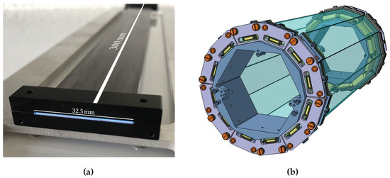
Figure 10.
(a) Prototype of a scintillating fiber ribbon, formed by staggering three layers of round scintillating fibers. (b) Structure of the SciFi detector, with the scintillating fiber ribbons shown in light blue [1].
The light produced in the ribbons is detected in SiPM column arrays at both fiber ends, which are coupled to the ribbons by simple mechanical pressure. Acquiring the signal on both sides improves the time resolution, enhances the signal-noise discrimination and increases the detection efficiency of the global system. Hamamatsu S13552-HRQ SiPM arrays are used, which were developed for the LHCb experiment. The SiPM sensor is segmented in 64 independent readout columns, denoted as channels. Each channel consists of 104 pixels of dimensions , arranged in a 4 × 26 grid. With a photon detection efficiency of up to 50%, the sensors can detect single photons and have a very fast instrinsic time response. Unirradiated sensors of this type present typical dark rates of ∼100 kHz per channel at room temperature. To reduce the dark counts and mitigate the radiation damage effects, they are cooled down to 0 °C with a water-cooling system installed in the support structure. The SiPM are read out with a dedicated mixed-mode Application Specific Integrated Circuit (ASIC), the MuTRiG (see Section 4.3), which digitizes the crossing time information at a single photon level. The chip generates about 1 W of thermal output, dissipated out with the same water-cooling system used for the SiPM.
The performance of a subset of SciFi ribbons was evaluated in test beam campaigns at CERN PS (T9 beamline) and PSI (M1 beamline). The signal waveforms were collected with fast pre-amplifier and readout digitizing electronics based on the DRS4 ASIC [13]. The waveforms were processed using algorithms close to the ones of the MuTRiG ASIC (see Section 4.3). In the data analysis, consecutive SiPM channels with an amplitude larger than a specific threshold (in this case the one corresponding to 0.5 photo-electrons) are clustered together. A multiplicity of at least two adjacent SiPM channels is required to form a cluster.
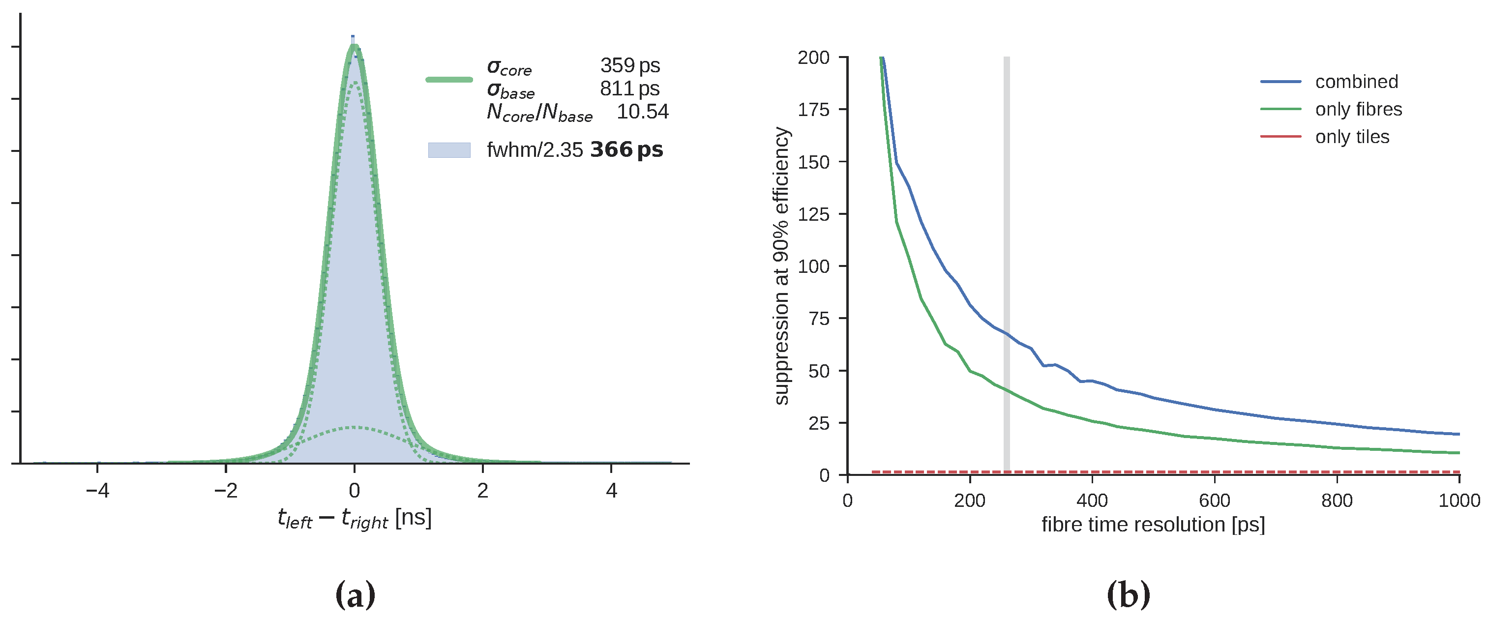
A 3-layer SCSF-78MJ ribbon without black epoxy presents a typical cluster size of around 3.5 channels per cluster for particles crossing the ribbon at 0. At an angle of 30, which is close to the mean crossing angle in Mu3e of 25, the average cluster size is 3.9 channels per cluster. This corresponds to an average yield of 17 photons recorded at each side of the ribbon. The cluster reconstruction efficiency for the aforementioned threshold and multiplicity is 95%, and reaches almost 100% with no timing requirements on the recorded signals. The overall timing performance is shown in Figure 11a. The spread of the time difference distribution from the two ribbon sides corresponds to twice the intrinsic detector resolution, meaning a time resolution of ps is measured. Figure 11b shows the background suppression power of the SciFi detector as a function of its time resolution, obtained from simulation. Considering a 250 ps resolution and 90% efficiency, an accidental background suppression of is achieved with the SciFi detector alone, reduced to when combined with the tiles detector (see Section 4.2). In the presence of only the tile detector, significant suppression is only achieved if all three particles of a candidate end up in this sub-detector.
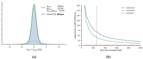
Figure 11.
(a) Time resolution of a SciFi ribbon defined as the difference between the time measured on both sides. The global time resolution is defined as ps. (b) Suppression of accidental background as a function of the fiber detector time resolution if only the fiber detector (green) is used or both timing detectors (blue) are used. The tile detector alone has no suppression power [1].
4.2. Tile Detector
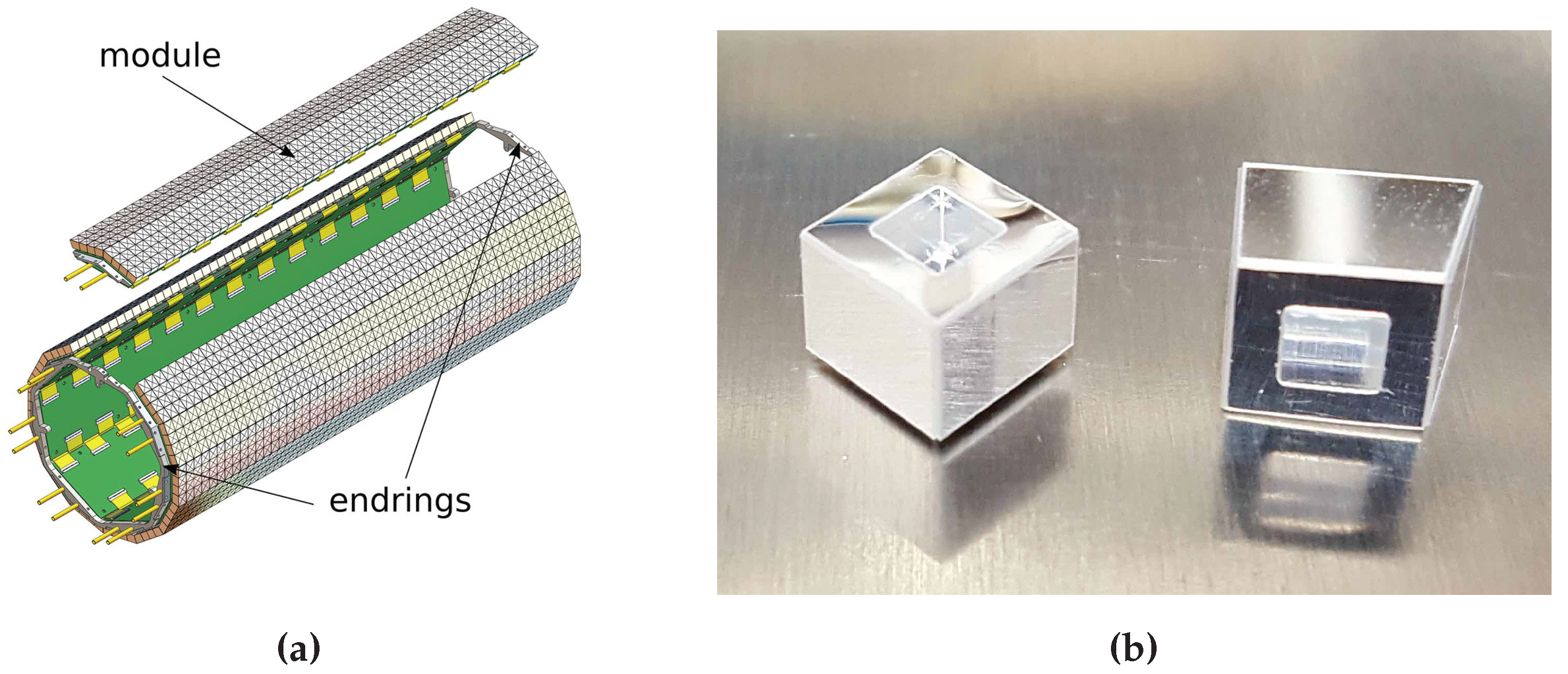
Located at the very end of the trajectories of the recurling particles, the tile detector is not subject to constraints on the amount of detector material, but suffers from tight space constraints. Towards the desired accidental background suppression, it must present a timing resolution better than 100 ps and a detection efficiency close to 100%. To fulfill these needs, the tile detector is composed of plastic scintillator segmented into high-granularity tiles, as shown in Figure 12a. Two identical stations are placed on each side of the Mu3e detector, one in each recurling station. They have the shape of a 34.2 cm long hollow cylinder enclosing the beampipe, with an outer radius of 6.4 cm, limited by the surrounding pixel layers. Providing the highest feasible channel density, each station is segmented into 52 tiles in the beam direction and 56 tiles along the azimuthal angle, each with a size of mm. Such granularity is essential to achieve high time resolution and low occupancy.
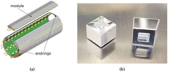
Figure 12.
(a) Structure of one station of the tiles detector, with the individual tiles shown as small squares. (b) Prototype of a scintillating tile wrapped with ESR foil [1].
The tiles are made out of Eljen technology EJ-228 plastic scintillator, which has a high light yield (10,200 photons per MeV) and a fast response time (0.5 ns rise time and 1.4 ns decay time), manufactured in the Kirchhoff-Institute for Physics in Heidelberg. Every tile is individually wrapped with Enhanced Specular Reflector (ESR) foil to increase the light yield and optically isolate the channel, as shown in Figure 12b. Each individual tile is read out by a mm SiPM produced by Hamamatsu (model S13360-3050VE). The SiPM presents 3600 pixels of size and is glued to the bottom of the tile. The signals from the tiles are collected and digitized with the MuTRiG ASICs, described in Section 4.3, as in the case of the fibers. The heat of the readout chips is dissipated via water-cooling through a copper tube in the support structure where the chips stand.
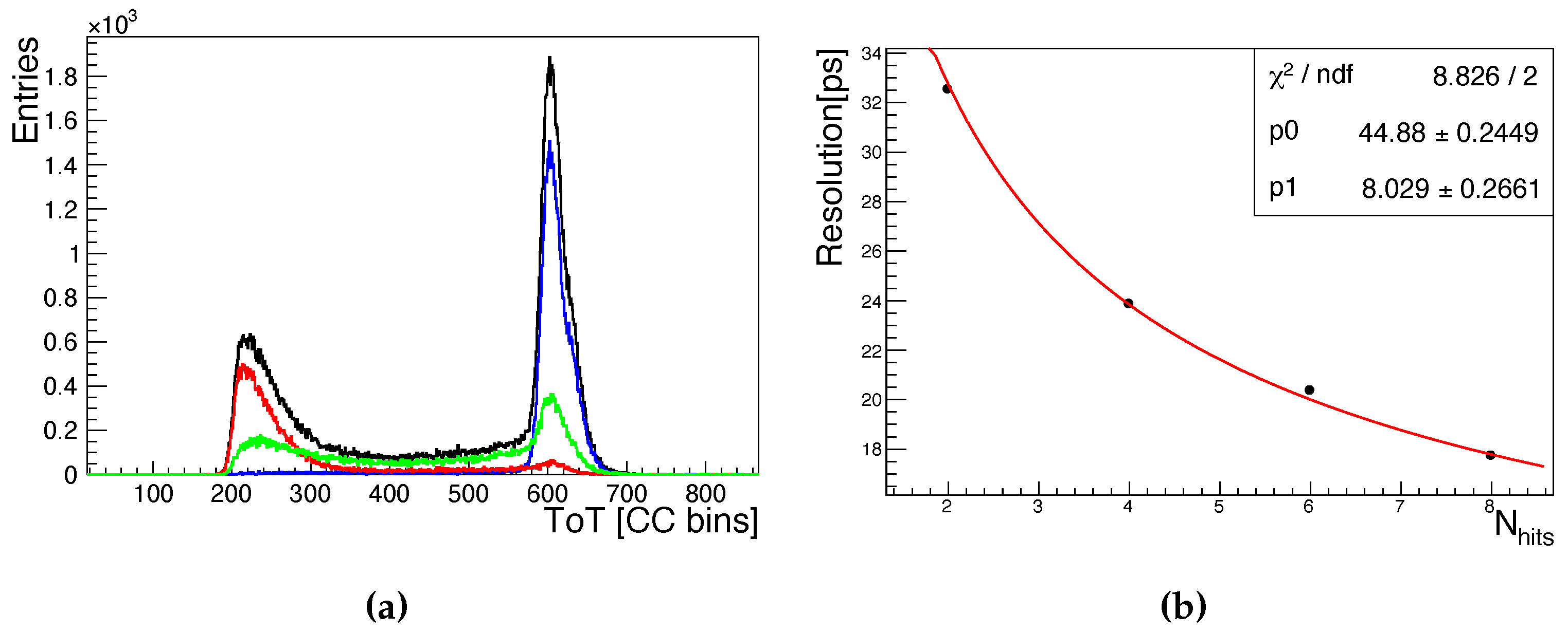
A technical prototype of the tile detector was developed in order to evaluate the time resolution and the detection efficiency. It was read out with a BGA packaged STiC 3.1, which has the same front-end as the MuTRiG ASIC. Three sub-modules consisting of 96 channels were assembled and tested with an electron beam at the DESY test-beam facility. The measured time-over-threshold (see Section 4.3) spectrum is presented in Figure 13a. It shows a sharp peak originating from electrons fully traversing the tile, demonstrating an excellent light collection. A secondary peak is also present: it is caused by cross-talk of neighbouring tiles, estimated by selecting hits where at least one direct neighbour has an energy deposition in the Landau peak. The secondary peak is largely separated from the signal thanks to the individual tile wrapping. The figure additionally shows the contribution from edge effects where particles pass only partially through the tile.
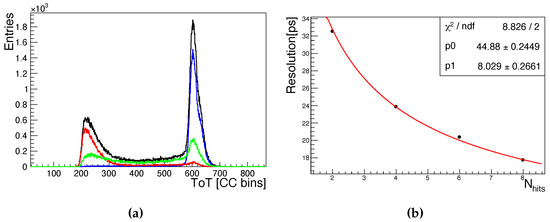
Figure 13.
(a) Energy deposition in a scintillator tile (black), composed of a Landau peak (blue), a plateau arising from edge effects (green) and a peak from optical cross-talk (red), as obtained from data by applying different geometrical cuts. The unit “CC bins” corresponds to the coarse counter bins above a certain threshold as computed by the readout chip (see Section 4.3). (b) Time resolution as a function of the number of hits per cluster. The fit is parametrized as [1].
In the same test beam campaign, a detection efficiency above 99% and an average time resolution of 45 ps were measured for all the tile detector channels. The average cluster size is around 2 activated channels per event, with cluster sizes as large as 9 being observed. Events with large channel multiplicity result in a better time resolution measurement, reaching values as low as 18 ps, as seen in Figure 13b.
4.3. MuTRiG Readout Chip
The signals from the fiber and the tiles subdetectors are read out with a common ASIC, the so-called MuTRiG, which stands for Muon Timing Resolver Including Gigabit-link. The chip was developed at the Kirchhoff Institute in Heidelberg as an evolutional development from the STiCv3.1 chip [14]. It is a 32 channel, mixed-signal SiPM readout ASIC designed and fabricated in UMC 180 nm CMOS technology. It extends the excellent timing performance of the STiCv3.1 chip with a newly developed fast digital readout to be able to cope with the high event rates (1 MHz/channel) expected for the fiber detector.
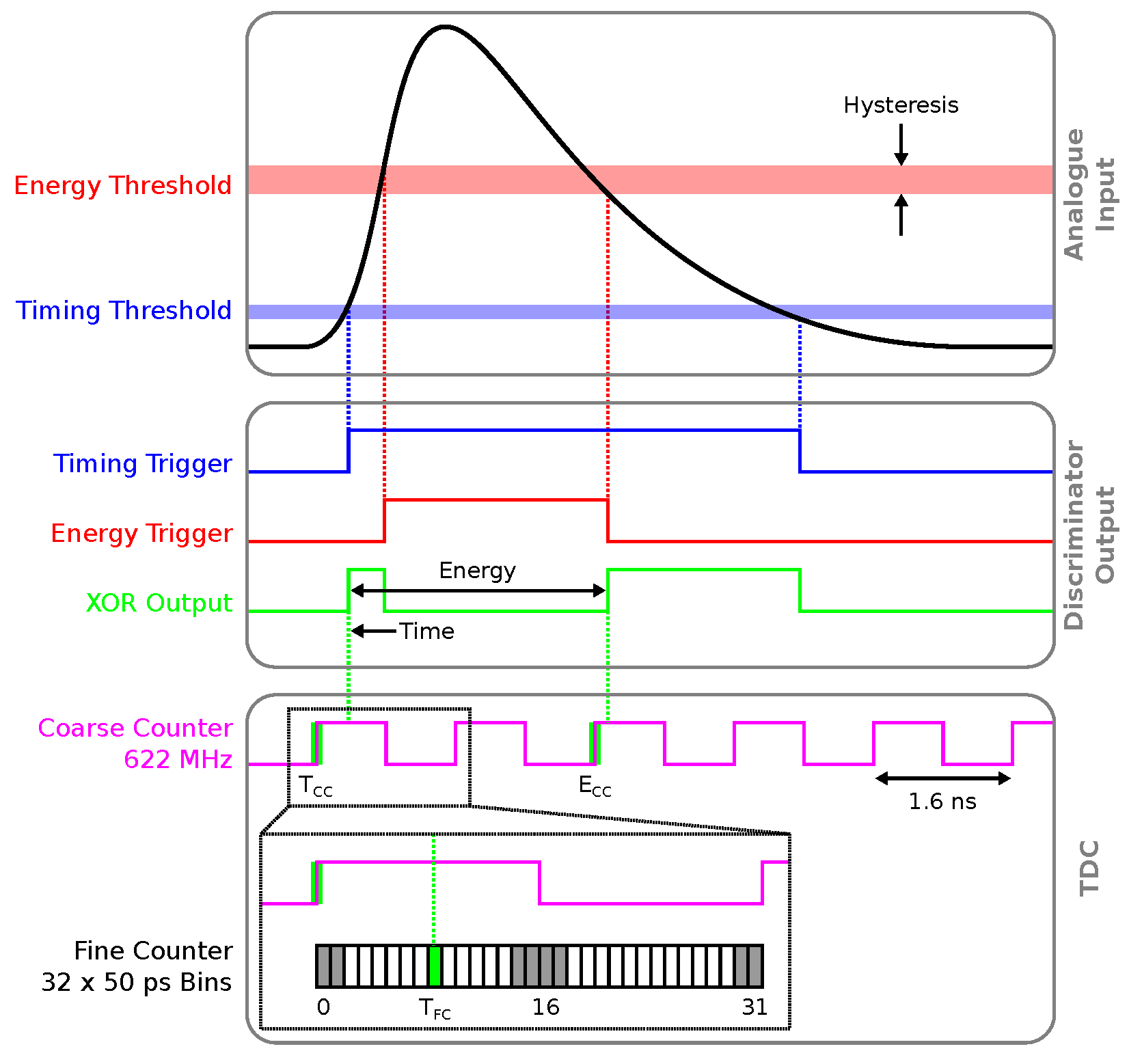
Figure 14 shows a sketch of the MuTRiG working principle. The analogue signals from SiPM are discriminated by a lower “time” (T) and an higher “energy” (E) thresholds. The ASIC digitizes the rising edge at the lower T-threshold and the time of the falling edge at the higher E-threshold into a T- and an E-timestamp, respectively. The T-timestamp corresponds to the signal’s time of arrival, while the difference between the two timestamps provides a linearized time-over-threshold. The T-threshold can be adjusted around the single photon level, whereas the E-threshold covers a much larger range up to typical SiPM saturation levels.
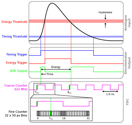
Figure 14.
Sketch of the MuTRiG chip functionality. The time and energy information of the analogue signal is obtained via two discriminator units, whose output is processed by a TDC with a 625 MHz coarse counter and a fine counter with a 50 ps beam size [1].
The excellent time resolution of the chip is granted by a fully differential analog front-end along with a 50 ps time binning time-to-digital converter (TDC). At the arrival of a hit signal above threshold, the TDC module digitizes the T- and E-timestamps by sampling the state of a 1.6 ns coarse-counter. The time resolution is further improved with an additional fine counter of 50 ps bin width, used to make a more precise measurement of the hit time within each bin of the coarse counter. To verify the timing performance, the MuTRiG was tested with the Mu3e tile detector prototype in an electron test beam campaign at DESY. Excellent channel-to-channel coincidence timing resolutions of less than 50 ps were measured over a large chip configuration parameter range, confirming the functionality of the chip.
In order to cope with high event rates, a double data rate serializer and a customized low-voltage differential signaling (LVDS) transmitter were developed for establishing a 1.25 Gbps data link for data transmission to the Data Acquisition system (DAQ), described in Section 5.1. To allow for higher event rate capabilities, the output event structure can be switched from the standard 48 bits, containing the T- and E-timestamps, to a shorter event structure of 27 bits, which records only the T-timestamp and a 1 bit energy flag indicating if the signal has passed the E-threshold. The former is used in the readout of the tile detector, while the latter is used in the fiber detector, subject to higher occupancy.
5. Data Acquisition and Services
5.1. DAQ
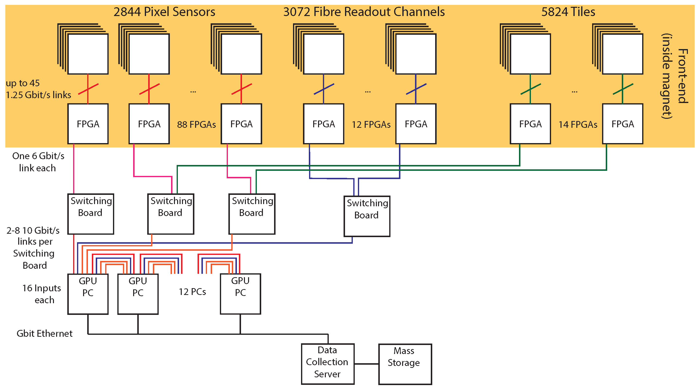
The Mu3e data acquisition system (DAQ) [15] works in continuous mode, i.e., without a hardware trigger. This implies that all subsystems continuously send zero-suppressed data. A sketch of the Mu3e DAQ is drawn in Figure 15.

Figure 15.
Mu3e DAQ scheme. The data received from the detectors are collected by dedicated front-end FPGAs inside the magnet, then delivered to switching boards where all detector hits are sorted and sent to a PC in the filter farm, where the events are reconstructed [1].
The data processing is performed in three stages: front-end FPGA boards [15], switching boards [16] and filter farm. The front-end boards collect the data from the subsystems, sort (also cluster in the case of SciFi) and package it, along with sending commands and monitoring the environment. The design of the front-end board is unique for all subsystems, and each board covers a specific portion of any given subdetector, depending on its design. The front-end boards are connected to backplanes located in Service Support Wheels (SSWs) at the edges of the experiment and controlled by crate controller boards. The SSWs also provide cooling via water-cooled heat pipes connected to the front-end boards through custom-made aluminum cooling plates. The data are sent through optical links from the front-end boards to the switching boards, which sit outside the experimental area. Here, the data from different subsystems are synchronized such that each PC of the filter farm receives hits from the whole detector. The filter farm consists of PCs equipped with FPGA boards, which are connected to the switching boards by optical links. The event data are read by the PCs via Direct Memory Access and copied to a GPU where the event reconstruction algorithms take place (vertex selection and track fitting). This data, along with slow control and environment data, is sent to the central DAQ computer. This runs the MIDAS (Maximum Integrated Data Acquisition System) software, which provides tools for event building and a slow control interface.
The DAQ relies on a very stable clock distribution for operating the many Gbit/s links and for precise timing measurements. This is provided by custom-designed boards. The global frequency is 125 MHz, which can be changed locally by phase-locked loops. Several tests show excellent performance, with an observed clock jitter of 5 ps, much less than the 10 ps required for stable operation [1].
5.2. Services
5.2.1. Power Distribution
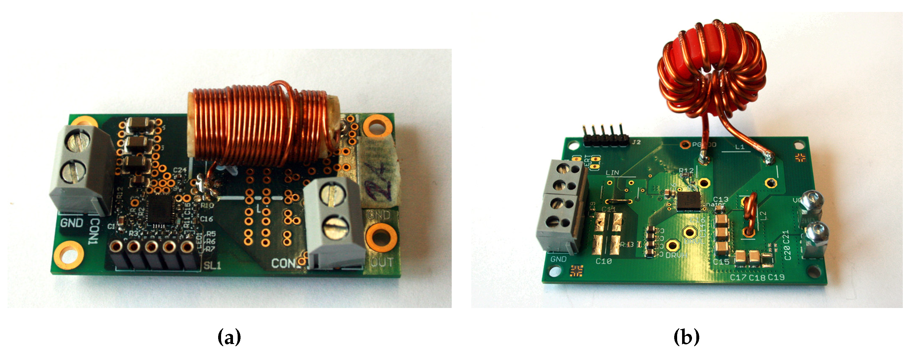
The Mu3e experiment is powered by 112 independent detector partitions. The power is supplied by TDK-Lambda GENESYS low voltage power supplies and then redistributed throughout the DAQ boards and the detector ASICS by means of custom-made power boards equipped with DC-DC converters. Since the power boards are meant to be used inside the magnetic field in a very dense service area, commercial compact high-power converters could not be used, as they have ferrite core inductor. The power boards for the front-end boards and the detector ASICs (both MuPix and MuTRiG ) can be seen in Figure 16a,b respectively. They were both successfully tested in magnetic fields, with Peak-Peak ripples of less than 10 mV. The power board for the detectors was also successfully tested with MuPix sensors [1].

Figure 16.
Power boards used for powering (a) front-end boards and (b) detector ASICs [1].
The high voltage necessary to operate the MuPix and the SiPMs is provided by custom-designed boards, based on the Cockroft-Walton voltage multiplier. These boards have been operated in high magnetic fields with no issues.
5.2.2. Cabling
The power is distributed inside the detector through solid copper cables of 2.5 mm gauge. Since all connections have to be done outside the detector acceptance, to reach the inner components only the space around the beampipe can be used. Here, copper rods with a cross-section of 5 × 2.5 mm are used, each insulated by the neighbouring one with a polyimide foil wrap, and held in place by epoxy.
The data are transmitted between detectors and front-end boards through micro-twisted pair cables. Each of these is a AWG 36 wire with a Polyimide isolation and an impedance of 90 Ω, and they are collected in bundles of 50 with a diameter of 2 mm.
6. Schedule and Physics Readiness
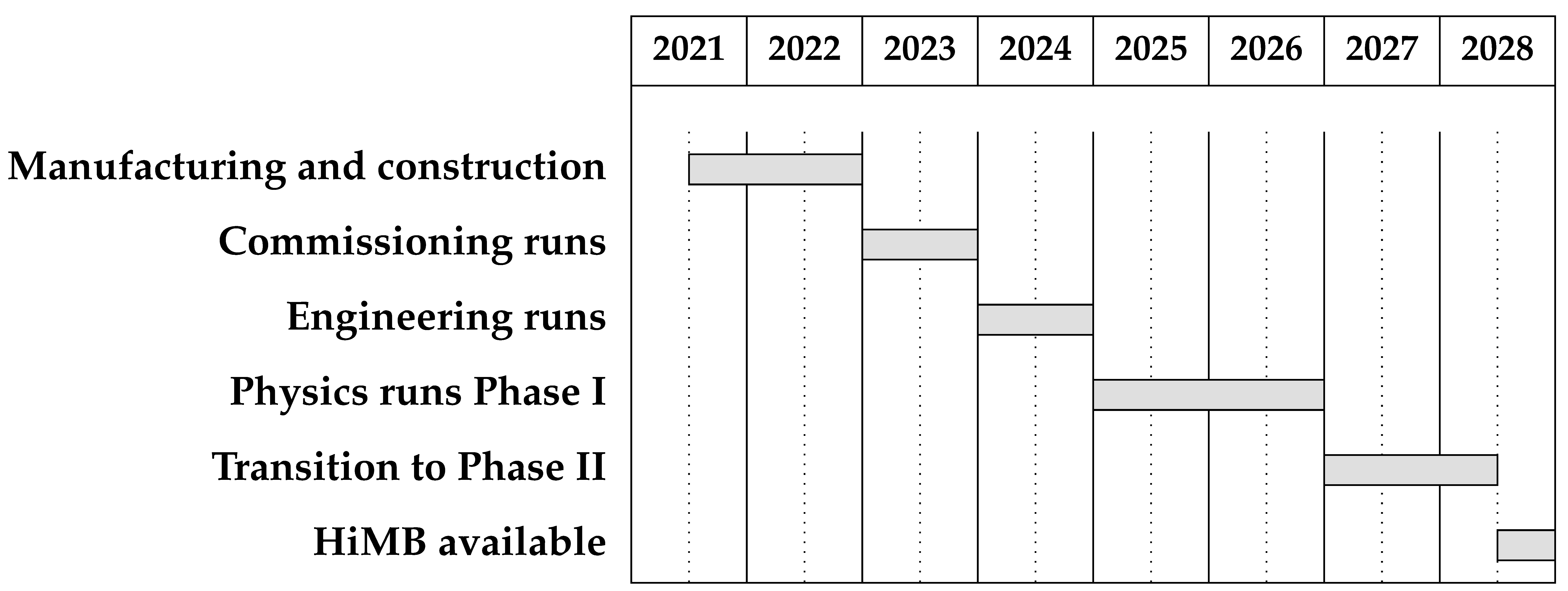
An simplified schedule for the Mu3e experiment during the period 2021 to 2028 is presented in Table 4. The manufacturing and construction of the detector is expected to be completed by the end of 2022. A series of commissioning runs are planned in 2023; they are aimed to install and test the performance of the various subdetector components before the production of the full Phase I detector. In preparation towards this phase, a first integration run of the Mu3e detector with muon beam took place in June 2021 at PSI. It comprised the pixel and fiber detectors partially installed inside the final magnet, addressing their mechanical integration and their electronics, as well as their operation and the data acquisition. The integration was successfully accomplished and a satisfactory low statistics readout of the pixel detector was achieved. Subsequent engineering runs in 2024 are expected to bring further understanding of the Mu3e detector as a whole and might provide a series of first physics observables such as the measurement of the muon decay spectrum.

Table 4.
Simplified operations schedule of the Mu3e experiment.
The actual physics production runs for Phase I is planned to take place in 2025 and 2026. During this period, continuous improvement of the detector operation and the analysis methods is foreseen. After this phase, Mu3e is expected to reach an unprecedented single event sensitivity of <. The present planning at PSI foresees a transition period towards Phase II, including a shutdown, which is planned during 2027 and the first half of 2028 and is aimed to install and commission the HiMB project. To fully exploit the new beam capabilities, the detector is expected to undergo an important upgrade, with longer stations and target to maximize the acceptance and allow for more precise energy and timing measurements. Phase II physics production runs are expected to start in the second half of 2028. The combined performance of the enhanced detector eventually leads to a single event sensitivity of <.
Author Contributions
Writing—review & editing, C.M.P. and L.V. All authors have read and agreed to the published version of the manuscript.
Funding
The Heidelberg groups acknowledge the support by the German Research Foundation (DFG) funded Research Training Groups HighRR (GK 2058) and “Particle Physics beyond the Standard Model” (GK 1994), by the EU International Training Network PicoSec (grant no. PITN-GA-2011-289355-PicoSEC-MCNet), by the International Max Planck Research School for Precision Tests of Fundamental Symmetries (IMPRS-PTFS) and the Heinz-Götze-Stiftung. The work of the Mainz group has also been supported by the Cluster of Excellence “Precision Physics, Fundamental Interactions, and Structure of Matter” (PRISMA EXC 1098 and PRISMA+ EXC 2118/1) funded by the German Research Foundation (DFG) within the German Excellence Strategy (Project ID 39083149). We acknowledge the contributions of the PRISMA Detector laboratory to the development of the DC-DC converters. The Swiss institutes acknowledge the funding support from the Swiss National Science Foundation grants no. 200021_137738, 200021_165568, 200021_172519, 200021_182031 and 20020_172706. The Particle Physics Department (DPNC) of the University of Geneva gratefully acknowledges support from the Ernest Boninchi Foundation in Geneva. The UK institutes thank the Science and Technology Facilities Council for funding their work through the Large Projects scheme, under grant numbers: ST/P00282X/1, ST/P002765/1, ST/P002730/1, ST/P002870/1. N. Berger, S. Shrestha, A. Kozlinskiy, A.-K. Perrevoort, D. vom Bruch, Q. H. Huang, U. Hartenstein and F. Wauters thank the DFG for funding their work on the Mu3e experiment through the Emmy Noether programme. F. Meier Aeschbacher, I. Perić, A. Schöning and D. Wiedner thank the DFG for funding their work under grant no. SCHO 1443/2-1. G. Hesketh gratefully acknowledges the support of the Royal Society through grant numbers UF140598 and RGF\EA\180081.
Acknowledgments
We gratefully acknowledge the beamtimes provided by the following facilities: test beam facility at DESY Hamburg (Germany), a member of the Helmholtz Association (HGF), M1 at Paul Scherrer Institut, Villigen (Switzerland), PS and SPS at CERN, Geneva, (Switzerland), and MAMI A2 and X1 at Institut für Kernphysik at the JGU Mainz (Germany). We gratefully acknowledge important contributions to the experiment, made by staff in the mechanical and electrical workshops and cleanroom facilities in all collaborating institutes.
Conflicts of Interest
The authors declare no conflict of interest.
References
- Arndt, K.; Augustin, H.; Baesso, P.; Berger, N.; Berg, F.; Betancourt, C.; Bortoletto, D.; Bravar, A.; Briggl, K.; vom Bruch, D.; et al. Technical design of the phase I Mu3e experiment. Nucl. Instrum. Methods Phys. Res. Sect. A 2021, 1014, 165679. [Google Scholar] [CrossRef]
- Calibbi, L.; Signorelli, G. Charged Lepton Flavour Violation: An Experimental and Theoretical Introduction. Riv. Nuovo Cim. 2018, 41, 71–174. [Google Scholar]
- Bellgardt, U. et al., [SINDRUM Collaboration] Search for the Decay μ+→e+e-e+. Nucl. Phys. 1988, 299, 1–6. [Google Scholar] [CrossRef]
- Baldini, A.M. et al., [MEG II Collaboration] The design of the MEG II experiment. Eur. Phys. J. C 2018, 78, 1–60. [Google Scholar] [CrossRef]
- Bartoszek, L.; Barnes, E.; Miller, J.P.; Mott, J.; Palladino, A.; Quirk, J.; Roberts, B.L.; Crnkovic, J.; Polychronakos, V.; Tishchenko, V.; et al. Mu2e Technical Design Report. arXiv 2015, arXiv:1501.05241. [Google Scholar]
- Experimental Proposal for Phase-I of the COMET Experiment at J-PARC. Available online: https://j-parc.jp/researcher/Hadron/en/pac_1207/pdf/E21_2012-10.pdf (accessed on 30 October 2021).
- Kiselev, D.; Baumann, P.; Duperrex, P.; Jollet, S.; Kettle, P.-R.; Knecht, A.; Laube, D.; Nyfeler, C.; Papa, A.; Reggiani, D.; et al. Progress and Challenges of the PSI Meson Targets and Relevant Systems. Available online: https://journals.jps.jp/doi/abs/10.7566/JPSCP.33.011102 (accessed on 30 October 2021).
- Kuno, Y.; Okada, Y. Muon decay and physics beyond the standard model. Rev. Mod. Phys. 2001, 73, 151–202. [Google Scholar] [CrossRef] [Green Version]
- Perić, I. A novel monolithic pixelated particle detector implemented in high-voltage CMOS technology. Nucl. Instrum. Methods Phys. Res. Sect. A 2007, 582, 876–885. [Google Scholar] [CrossRef]
- Augustin, H.; Berger, N.; Dittmeier, S.; Immig, D.M.; Kim, D.; Mandok, L.; Gonzalez, A.M.; Menzel, M.; Noehte, L.O.S.; Perić, I.; et al. MuPix10: First Results from the Final Design. Available online: https://journals.jps.jp/doi/abs/10.7566/JPSCP.34.010012 (accessed on 30 October 2021).
- LTU, LED Technologies of Ukraine. Available online: http://ltu.ua/en/index/ (accessed on 30 October 2021).
- Rudzki, T.; Augustin, H.; Deflorin, M.; Dittmeier, S.; Frauen, F.; Immig, D.M.; Kim, D.; Aeschbacher, F.M.; González, A.M.; Menzel, M.; et al. The Mu3e experiment: Toward the construction of an HV-MAPS vertex detector. arXiv 2021, arXiv:2106.03534. [Google Scholar]
- Ritt, S. Design and performance of the 6 GHz waveform digitizing chip DRS4. In Proceedings of the 2008 IEEE Nuclear Science Symposium Conference Record, Dresden, Germany, 19–25 October 2008; pp. 1512–1515. [Google Scholar]
- Shen, W.; Harion, T.; Chen, H.S.; Briggl, K.; Stankova, V.; Munwes, Y.; Schultz-Coulon, H.-C. A silicon photomultiplier readout ASIC for time-of-flight application using a new time-of-recovery method. IEEE Trans. Nucl. Sci. 2018, 65, 1196–1202. [Google Scholar] [CrossRef]
- Augustin, H.; Berger, N.; Bravar, A.; Briggl, K.; Chen, H.S.; Corrodi, S.; Dittmeier, S.; Gayther, B.; Gerritzen, L.; Gottschalk, D.; et al. The Mu3e Data Acquisition. IEEE Trans. Nucl. Sci. 2021, 68, 1833–1840. [Google Scholar] [CrossRef]
- Cachemiche, J.P.; Duval, P.Y.; Hachon, F.; Le Gac, R.; Réthoré, F. The PCIe-based readout system for the LHCb experiment. J. Instrum. 2016, 11, P02013. [Google Scholar] [CrossRef] [Green Version]
Publisher’s Note: MDPI stays neutral with regard to jurisdictional claims in published maps and institutional affiliations. |
© 2021 by the authors. Licensee MDPI, Basel, Switzerland. This article is an open access article distributed under the terms and conditions of the Creative Commons Attribution (CC BY) license (https://creativecommons.org/licenses/by/4.0/).


