Article

Research on Phase Current Reconstruction for DPWM2 of Induction Motor Drive System Based on DC-Link Current Sampling

1
College of Electrical Engineering, Southwest Minzu University, Chengdu 610225, China
2
Institute of National Productivity Development, Southwest Minzu University, Chengdu 610225, China
*
Author to whom correspondence should be addressed.
Machines 2022, 10(11), 1104; https://doi.org/10.3390/machines10111104
Submission received: 26 October 2022 / Revised: 10 November 2022 / Accepted: 13 November 2022 / Published: 21 November 2022
(This article belongs to the Section Electromechanical Energy Conversion Systems)

Abstract

:
In order to reduce the switching loss and cost, as well as improve the reliability of the induction motor (IM) drive system, the technology involving the three-phase current reconstruction of 60° discontinuous pulse width modulation (DPWM2) is studied in this paper. According to the analysis of the switching state for DPWM2 in different sectors, the three-phase current can be constructed by sampling the voltage of the DC-link resistor. When the target voltage vector is located near the sector boundary or in the low-modulation area, the duration of the active vector in the sampling period is less than the voltage sampling time, which leads to measurement errors of the DC-link current. Therefore, on the basis of the switching state in different unmeasured areas, a time compensation method combining phase shifting and frequency reduction is proposed, and the expressions for comparing values are derived. Lastly, a simulation model and an experimental platform are established to validate the accuracy of the proposed method.

1. Introduction

According to the characteristics of DC-side power supply, inverters can be divided into two types, i.e., voltage-source inverters (VSIs) and current-source inverters (CSIs) [1,2]. Among them, VSIs have high reliability and a simple modulation strategy; thus, they have been widely applied and studied [3,4]. In order to improve the voltage utilization and conversion efficiency of VSIs, in recent years, many scholars have performed in-depth studies on key issues such as switching loss, junction temperature, and life span [5,6]. Furthermore, considering traditional SPWM and SVPWM, many scholars have analyzed and explored discontinuous pulse width modulation (DPWM) technology [7,8,9].
In the development of motor drive control, an accurate current measurement is a necessary condition to obtain the excellent control performance of the motor, and two or three current sensors are generally needed to detect the three-phase stator current of the motor [10]. In addition, a current sensor is required to detect the DC-link current for short-circuit information detection and protection. However, the use of too many current sensors increases the economic cost of the motor drive system. Once a fault occurs in a current sensor, the motor does not operate properly [11]. To improve reliability and reduce cost, the technology involving phase current reconstruction based on the voltage sampling of a DC-link single resistor has been extensively researched. However, the algorithm implementation of phase current reconstruction is more complicated, as a function of the following problems:
(1)
The DC-link current is zero during the period of the zero vector; thus, the DC-link current can only be detected during the active vector [12];
(2)
When the switching state changes, it takes some time for the DC-link current to become stable, while the duration of the analog-to-digital conversion should also be considered. Therefore, it is necessary to ensure that the duration of the active vector takes the above into account [11];
(3)
The sampling moment may be in the oscillation stage or in the period of zero vector, which can induce serious errors in the sampling current, leading to the failure of phase current reconstruction [13];
(4)
When the target voltage vector is located near the sector boundary or in the low-modulation area, the duration of one or two active vectors is too short to sample the DC-link current [14]. In this paper, both the sector boundary and the low-modulation area are considered unmeasured areas.
In order to solve the above problems, some methods have been proposed in the literature. A discrete filtering algorithm was used in [15] to remove the rapidly changing sampling current, thereby obtaining a more accurate sampling current; however, this method may reduce the dynamic performance of the system. For situations where the deviation of the sampling current is large, a model-based current observer was introduced in [16] to improve the accuracy near the sector boundary; however, the observation model was too sensitive to the motor parameters. In [17], the sampling range was expanded by adding additional active vectors on the premise that the output voltage vector remains unchanged; however, the switching number and the current ripple increased. In [13], a single-pulse signal was injected into the non-observation area; hence, the three-phase currents could be reconstructed according to the fluctuation of the DC-link current. In [18], the phase current reconfiguration was optimized by improving the measurement topology, and a good reconstruction performance was obtained when the output voltage vector was in the low-modulation area. In [19], the duration of the active vector at the sampling instant was extended by changing the switch state of the SVPWM. Compared with other methods, this method is easy to implement; however, it is not suitable for DPWM.
In this paper, the principle and the switching state of the 60° discontinuous modulation (DPWM2) strategy are analyzed, and the methods of DC-link current sampling and phase current reconstruction are presented. Then, to solve the problem that the duration of one or two active vectors in sampling period is too short to sample the DC-link current, a time compensation method is proposed. Lastly, simulations and the experimental validation of the proposed method are performed.

2. Topology and Control Scheme

2.1. Topology of IM Fed by Voltage Source Inverter

Figure 1 shows the topology of the induction motor (IM) drive system fed by the three-phase voltage source inverter (VSI), where udc is the DC-link voltage, Cdc is the DC-link capacitor, S1–S6 are the power switching devices, and ia, ib, and ic are the three-phase stator currents of the IM. In particular, Rdc is the sampling resistor, the DC-link current is obtained by sampling the voltage of Rdc to reconstruct the three-phase currents.

2.2. Vector Control Scheme for the IM Fed by VSI

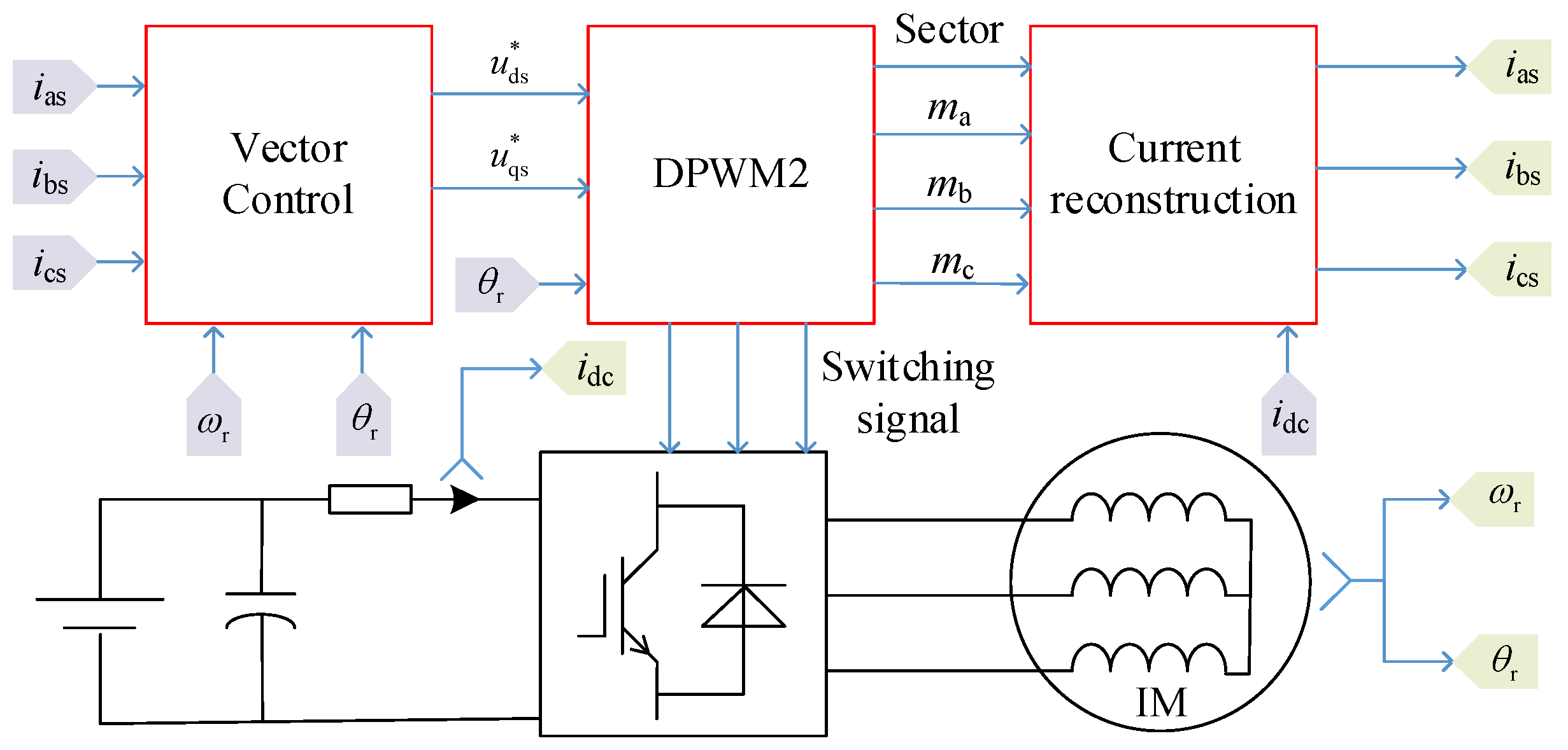
In the synchronous rotating frame (d–q axis) based on rotor flux orientation, the block diagram of the vector control scheme for the IM fed by VSI is shown in Figure 2. After executing the speed, the current inner loop, and the flux outer loop controllers, respectively, the command values of the stator voltages in the d–q axis u d * and u q * are obtained. In order to reduce the switching losses, DPWM2 is employed to generate the switching signals of S1–S6.

3. Switching Signal Generation Method of DPWM2

Firstly, by substituting u d * , u q * , and θr into Formula (1), the stator voltages u α * and u β * in the two-phase rotating coordinate frame can be obtained.
u α * = u d * cos θ r u q * sin θ r u β * = u d * sin θ r + u q * cos θ r
Then, the amplitude U and angle θ of the target voltage vector can be calculated as
U = ( u α * ) 2 + ( u β * ) 2 θ = arctan ( u β * / u α * )
Under different θ, the modulation function of DPWM2 is shown in Table 1, where ma, mb, and mc are the modulation ratio functions for phases a, b, and c, and M is defined as U/udc. The waveforms of ma, mb, and mc in one carrier period are presented in Figure 3. It can be seen that ma, mb, and mc reach 1 or −1 alternately, and the switching devices of each phase bridge arm do not act for two 1/6 cycles.
The switching sequences of DPWM2 in one carrier period under different sectors are depicted in Figure 4, which contains five segments. In Sectors I, III, and IV, 111 is utilized as the zero vector, which is located in the middle of the whole sequences. In Sectors II, IV, and VI, 000 is utilized as the zero vector, which is located in the front and end of the whole sequences. In Figure 4, T0, T1, and T2 represent the dwell time of the zero vector, the first active vector, and the second active vector, respectively. Additionally, Sa, Sb, and Sc represent the switching state of the three-phase bridges.

4. Phase Current Reconstruction Method Based on Single Resistor Sampling

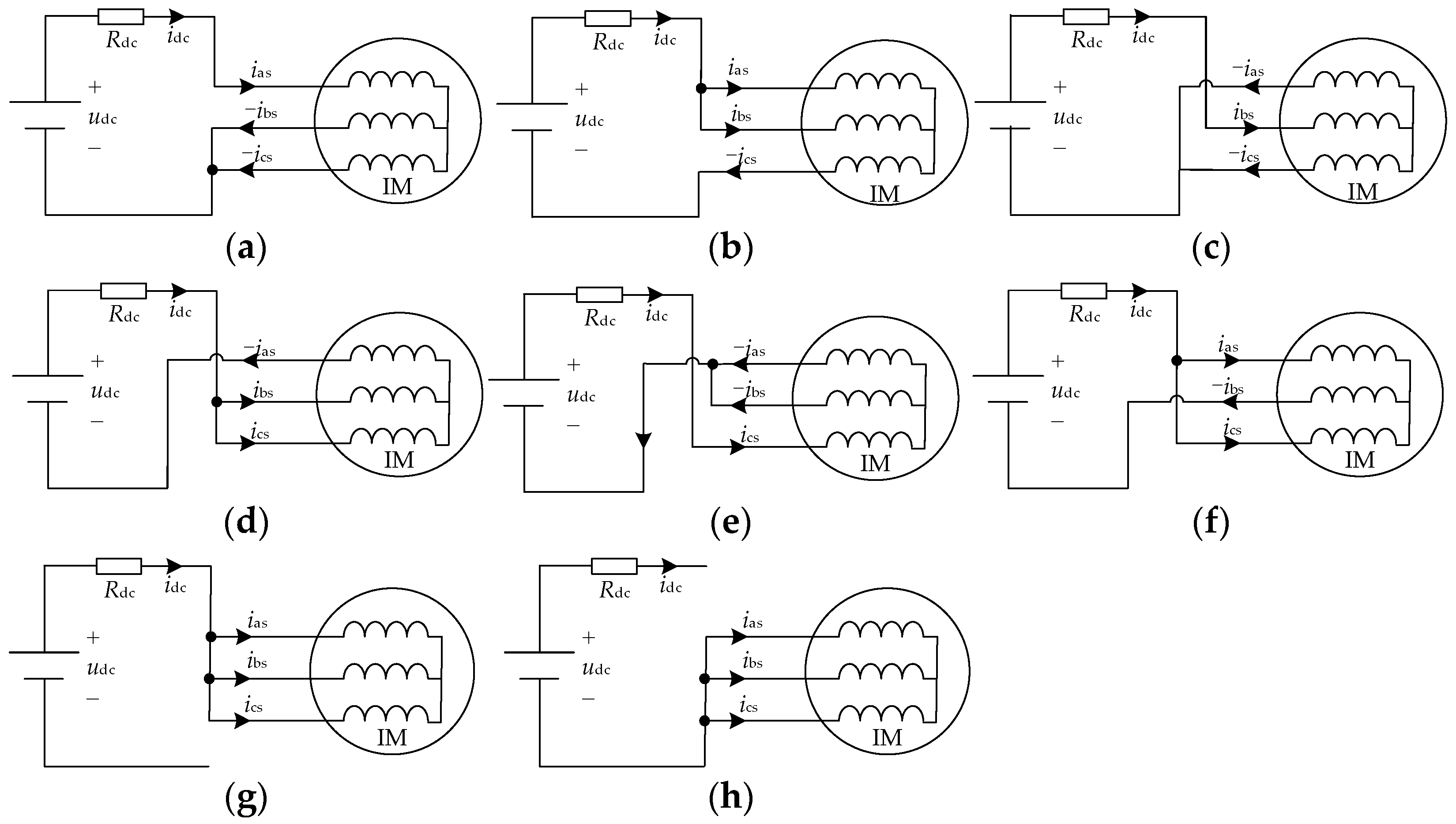
Figure 5 shows the equivalent circuits of IM fed by VSI under different switching states. In the switching state of the active vector, one phase current can be obtained from idc. In the switching state of the zero vector, idc is equal to zero, so the DC-link current cannot be detected during the switching state of the zero vector. According to Figure 5, the relationship between idc and the three-phase currents is summarized in Table 2.
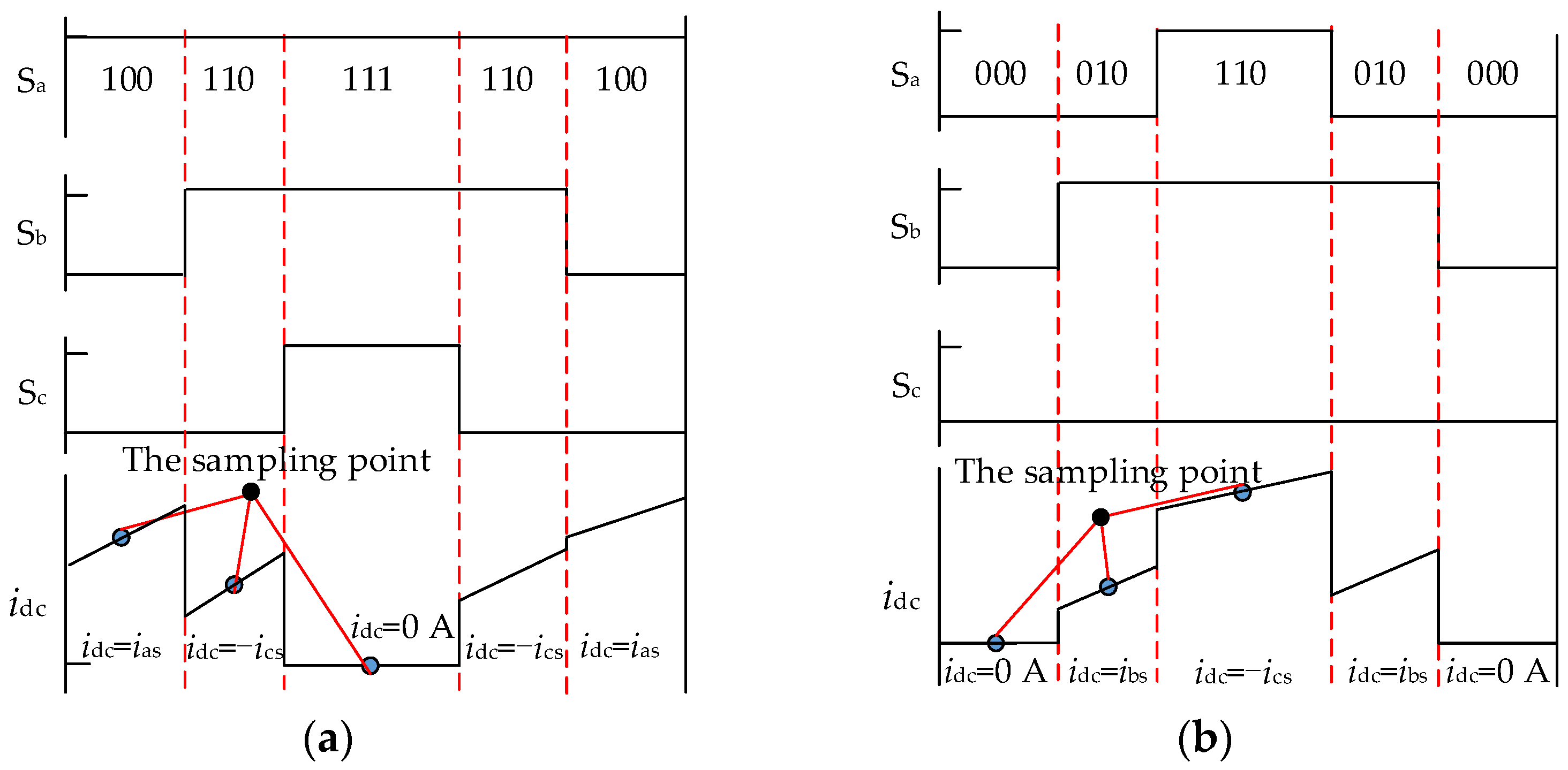
Firstly, to demonstrate the method for the three-phase current reconstruction of DPWM2 based on the DC-link current sampling, Sector I is taken as an example. The diagram is shown in Figure 6a. In the first half of the carrier period, three times of sampling are carried out in the switching states of 100, 110, and 111, respectively. Since the DC-link current is constantly changing during the active vector time, aiming to obtain the average current in each sequence, sampling is carried out at the middle time of each active vector, and the sampling current in the stage of zero vector is used to obtain the offset. Since the sum of the three-phase currents is equal to zero, the relationship between the three-phase currents and three-time sampling current (idc(k + 1), idc(k + 2), idc(k + 3)) can be described as
i a ( k ) = i dc ( k + 1 ) i dc ( k + 3 ) i b ( k ) = i dc ( k + 1 ) + i dc ( k + 2 ) + 2 i dc ( k + 3 ) i c ( k ) = i dc ( k + 2 ) i dc ( k + 3 )
The diagram of the three-phase current reconstruction in Sector II is shown in Figure 6b. Different from Sector I, the first current sampling occurs in the stage of zero vector, and according to Figure 4b, Figure 5b, Figure 6b, the relationships between the three-phase currents and three-time sampling current are described as
i a ( k ) = 2 i dc ( k + 1 ) i dc ( k + 2 ) + i dc ( k + 3 ) i b ( k ) = i dc ( k + 2 ) i dc ( k + 1 ) i c ( k ) = i dc ( k + 3 ) i dc ( k + 1 )
Similarly, the expressions of three-phase currents in Sectors III–VI can be derived and shown as Formulas (5)–(8), respectively.
i a ( k ) = i dc ( k + 2 ) i dc ( k + 3 ) i b ( k ) = i dc ( k + 1 ) i dc ( k + 3 ) i c ( k ) = i dc ( k + 1 ) + i dc ( k + 2 ) + 2 i dc ( k + 3 )
i a ( k ) = i dc ( k + 3 ) i dc ( k + 1 ) i b ( k ) = 2 i dc ( k + 1 ) i dc ( k + 2 ) + i dc ( k + 3 ) i c ( k ) = i dc ( k + 2 ) i dc ( k + 1 )
i a ( k ) = i dc ( k + 1 ) + i dc ( k + 2 ) + 2 i dc ( k + 3 ) i b ( k ) = i dc ( k + 2 ) i dc ( k + 3 ) i c ( k ) = i dc ( k + 1 ) i dc ( k + 3 )
i a ( k ) = i dc ( k + 2 ) i dc ( k + 1 ) i b ( k ) = i dc ( k + 3 ) i dc ( k + 1 ) i c ( k ) = 2 i dc ( k + 1 ) i dc ( k + 2 ) + i dc ( k + 3 )

5. Sampling Time Compensation Method for Unmeasured Areas

According to the above analysis, the DC-link current sampling during the switching states of the active vector should be completed twice within the half period of carrier signal rising. However, in the process of actual current sampling, a time delay occurs in the switching device action and A/D conversion, and the DC-link current also has an oscillating process. Therefore, the duration of the active vector should not be less than Tmin, which is the minimum current sampling time. Tmin is defined as follows:
T min = T dead + T set + T AD
where Tdead is the total time of the switching delay and the dead time, Tset is the time of the DC-link current achieving to steady state, and TAD is the time of A/D conversion.
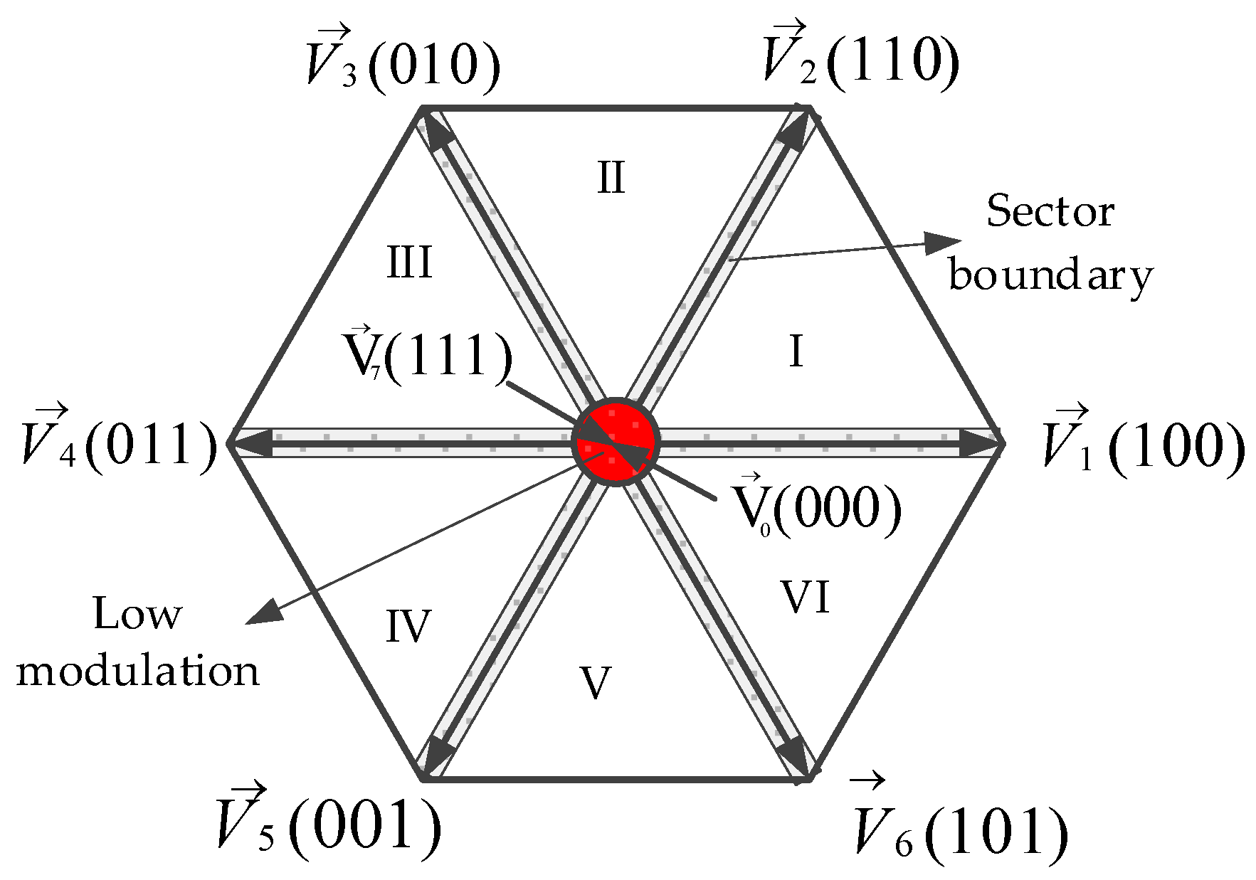
It can be seen from Section 4 that the vector order of odd sectors is different from that of even sectors. Meanwhile, different sector boundaries have different active vectors whose duration time is less than Tmin, and therefore, a variety of situations need to be discussed. If the target voltage vector is located in the areas of the sector boundary, the duration of an active vector will be less than Tmin. If the target voltage vector is located in the low modulation, the duration of both active vectors is less than Tmin, and phase current reconstruction cannot be completed under the above two conditions. The areas of the sector boundary and low modulation is shown in Figure 7.
Next, the time compensation methods for the active vector under different conditions will be described.

5.1. Time Compensation Methods in the Area near the Sector Boundary

Sectors I and II are taken as an example to discuss the time compensation method in different conditions; the areas near the sector boundary are divided into four regions, as shown in Figure 8.

5.1.1. Target Voltage Vector in Region 1

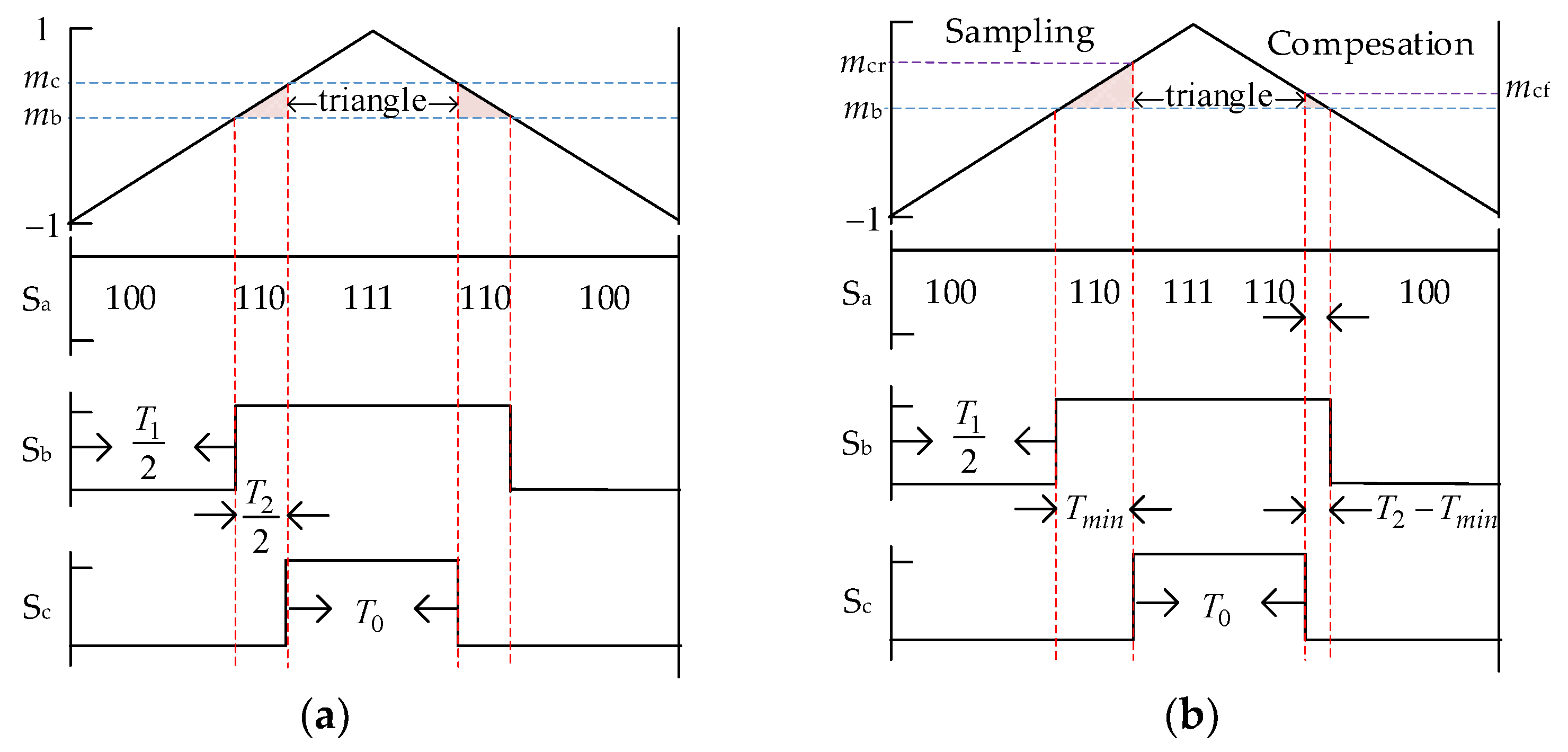
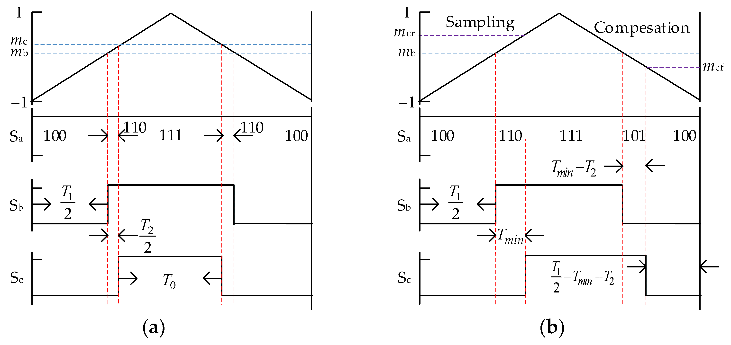
The rising stage of the carrier is noted as the sampling period, and the falling stage is noted as the compensation period. When the target vector V ref is located in Region 1, T2, the duration of V 2 is less than Tmin. If T2  (Tmin, 2Tmin), a simple phase-shifting method can be adopted to guarantee the duration of V 2 in the sampling period is equal to Tmin, and the duration of V 2 in the compensation period is equal to (T2 Tmin); the switching state in a carrier period is shown in Figure 9. It can be seen that there is no change in the duration of any vector. It is worth noting that the comparison value of phase-c in the rising stage of carrier is not the same as that in the falling stage. The triangle in Figure 9a is similar to that in Figure 9b, so the comparison value in the rising stage mcr and in the falling stage mcf should be satisfied as
m cr m b T min = 2 ( m c m b ) T 2 = 4 T s m cf m b T 2 T min = 2 ( m c m b ) T 2 = 4 T s
where Ts is the carrier period, and the mcr and mcf can be obtained as
m cr = m c + 4 T s T min T 2 2 m cf = m c 4 T s T min T 2 2
When T2 is less than Tmin, the diagram of phase shifting is shown in Figure 10. The duration of V 2 in one sampling period is set to Tmin, and the falling edge of Sc is later than Sb, so a new active vector V 6 appears, and the duration of V 6 is Tmin  T2. According to Figure 10b, the synthetic voltage vector one sampling period V s can be expressed as
V s = T 1 2 T s V 1 + T min T s V 2
where Ts is the carrier period. The synthetic voltage vector in one sampling period V c can be expressed as
V c = T min T 2 T s V 6 + T 1 + 2 T 2 2 T min 2 T s V 1
V 6 can be expressed as
V 6 = V 1 V 2
According to Formulas (11)–(13), V s + V c can be obtained as
V s + V c = T 1 T s V 1 + T 2 T s V 2
which is equal to V ref . The slope of the triangular carrier is 4/Ts, according to the similar triangle relationship, which is the same as Formula (10), and the expressions of mcr and mcf can be expressed as
m cr = m c + 4 T s T min T 2 2 m cf = T 1 + 2 T 2 2 T min T 1 + T 2 m c

5.1.2. Target Voltage Vector in Region 2

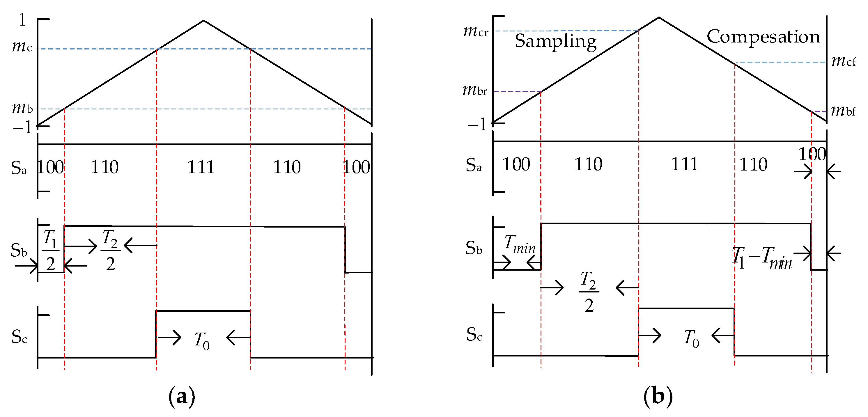
When the target vector V ref is located in Region 2, T1, the duration of V 1 is less than Tmin. If T1 belongs to the range (Tmin, 2Tmin), the duration of V 1 in one sampling period will be adjusted to Tmin, and the duration of V 1 in the sampling period will be equal to T1   Tmin; the switching state in a carrier period is shown in Figure 11. At this time, the switching state waveforms of phase-b and phase-c are no longer symmetrical in a carrier period. The expressions of the phase-b comparison value in the rising stage mbr and the comparison value in the falling stage mbf are expressed as
m br = m b + 4 T s T min T 1 2 m bf = m b 4 T s T min T 1 2
and the expressions of mcr and mcf are expressed as
m cr = m c + 4 T s T min T 1 2 m cf = m c 4 T s T min T 1 2
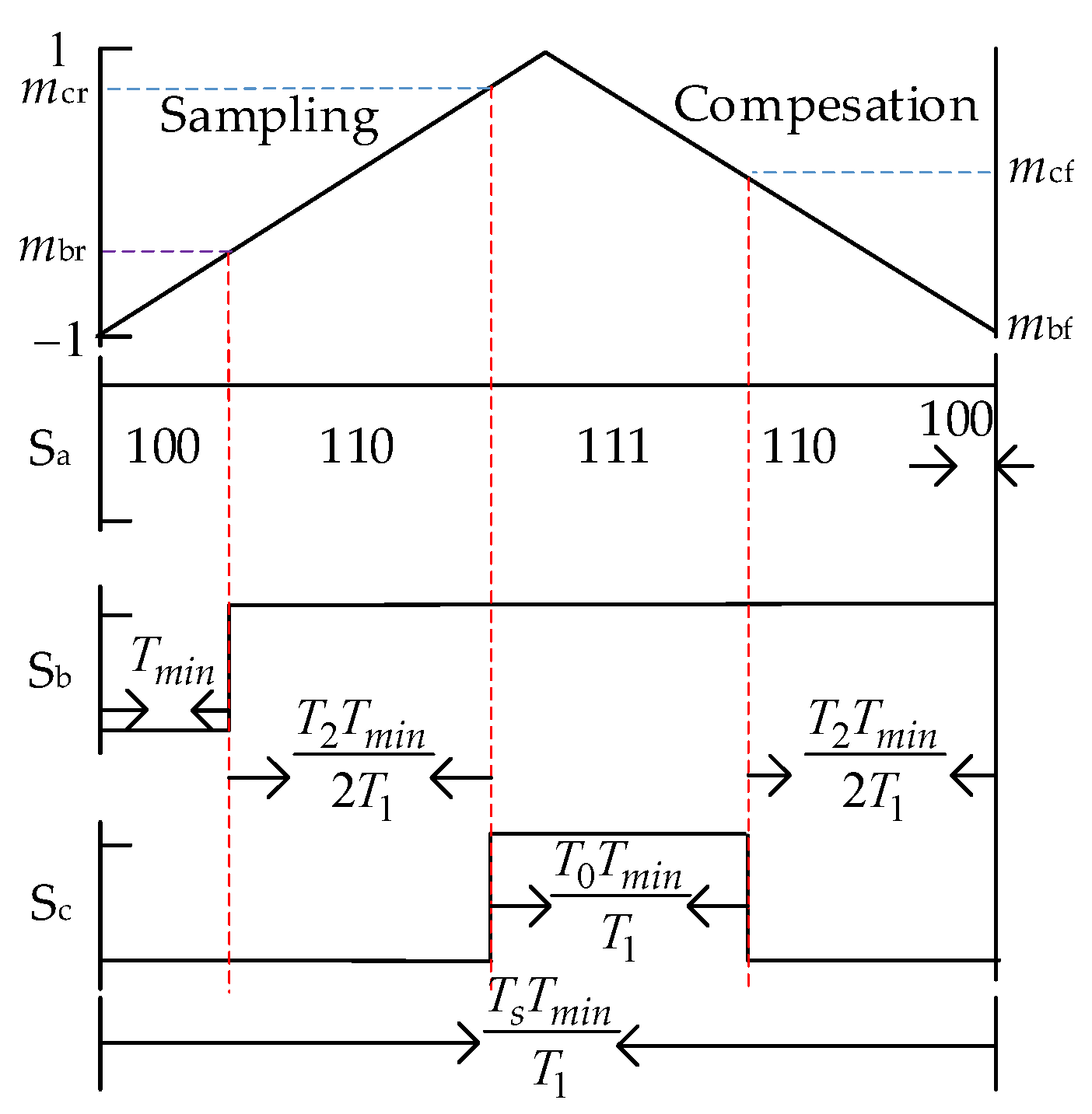
Different from Region 1, when T1 is less than Tmin, if the duration of V 1 in the sampling period is set to Tmin, the voltage error will not be able to be eliminated by adjusting the duration and phase of V 0 and V 2 . In order to solve this problem, a modulation method combining phase shifting and frequency reduction is proposed in this paper. The carrier period increases to TsTmin/T1. The diagram is shown in Figure 12. The value of mbr is the same as Formula (17), and mbf is equal to zero. mcr and mcf can also be expressed as Formula (18). If the target vector is near the boundary of Sectors III and IV, the time compensation method of phase shifting and frequency reduction are shown in Figure 9, Figure 10, Figure 11, Figure 12 and Figure 13, and the calculation method for the comparison value is shown in Formulas (11), (16) and (18).

5.1.3. Target Voltage Vector in Region 3

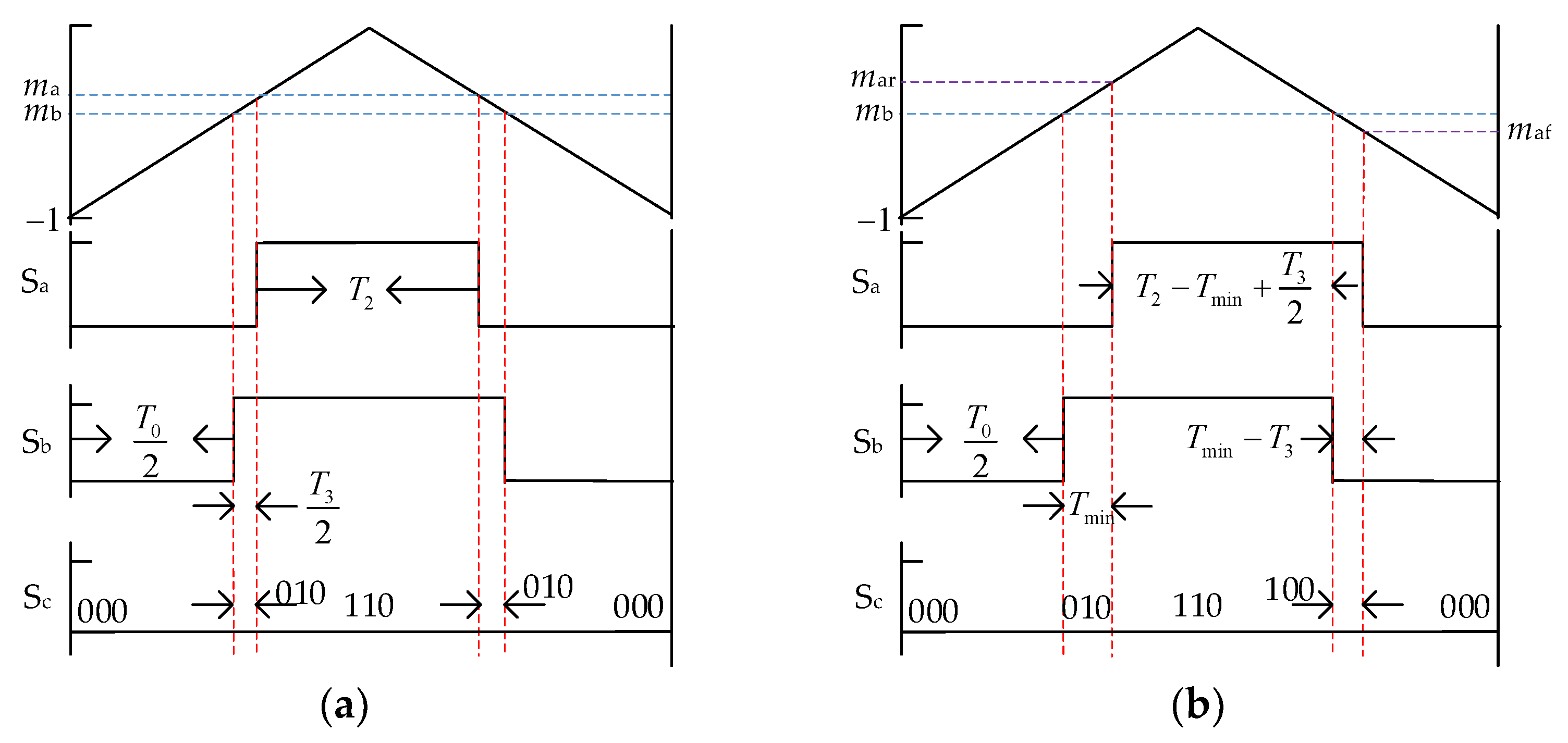
When V ref is located in Region 3, T3, the duration of V 3 (100), is less than Tmin. If T3 belongs to the range (Tmin, 2Tmin), the duration of V 1 in one sampling period will be adjusted to Tmin, and the duration of V 3 in one sampling period will be equal to T3   Tmin; this method is the same as that of Regions 1 and 2, and there is no change in the duration of any vector. If T3 is less than Tmin, the duration of V 3 in one sampling period is set to Tmin, and the falling edge of Sa is later than Sb, so a new active vector V 1 (100) appears, and the duration of V 1 is Tmin  T2. Due to V 2 = V 1 + V 3 , the error caused by the increase V 3 can be eliminated by V 1 , and the synthetic voltage vector is equal to V ref ; the switching state in one carrier period is depicted in Figure 13. The expressions of the comparison value of phase-a in the rising stage mar and the comparison value in the falling stage maf are expressed as
m ar = m a + 4 T s T min T 2 2 m af = T 3 + 2 T 2 2 T min T 3 + T 2 m a

5.1.4. Target Voltage Vector in Region 4

When V ref is located in Region 4, T2, the duration of V 2 (010) is less than Tmin. Since V 2 is a continuous vector, The case that T2 belongs to the range (Tmin, 2Tmin) should not be considered. However, if T2 is less than Tmin, and the duration of V 2 in one sampling period is set to Tmin, the voltage errors will be generated and unable to be eliminated by phase shifting alone. Therefore, the modulation method combining phase shifting and frequency should be adopted; the diagram is shown in Figure 14. After the carrier period expands to TsTmin/T1, all switching-state waveforms in one carrier period are symmetrical, and the comparison values do not need to be adjusted.

5.2. Time Compensation Methods in the Area of Low Modulation

When V ref is located in the area of low modulation, the duration times of the two active voltage vectors are less than Tmin. To ensure that the DC-link current can be sampled in the stages of two active vectors, the segments of the active voltage vectors are combined and placed in the sampling stage, and the carrier period is increased. The specific methods are as follows:

5.2.1. Target Voltage Vector in the Area of Low Modulation Belonging to Sector I

After phase shifting and carrier frequency reduction, the diagram of the switching state is shown in Figure 15. The carrier period is expanded to TsTmin/Tmin12, where Tmin12 is the minimum of T1 and T2. T 1 * and T 2 * are the new duration times of V 1 and V 2 and are defined as
T 1 * = T min ,   T 2 * = T 2 T min / T 1 T 1 T 2 T 1 * = T 1 T min / T 2 ,   T 2 * = T min T 1 > T 2
Both mbf and mcf are set to zero, and mbr and mcr are expressed as
m br = m b T 1 * T 1 m cr = m c ( T 1 * + T 2 * ) T 1 + T 2
When V ref is located in the area of low modulation belonging to Sectors III and V, the method of time compensation and comparison value calculation is the same as that in Sector I.

5.2.2. Target Voltage Vector in the Area of Low Modulation Belong to Sector II

After phase shifting and switching frequency reduction, the diagram of the switching state is shown in Figure 16. T 2 * and T 3 * are the new duration times of V 2 and V 3 and are defined as
T 2 * = T min ,   T 3 * = T 3 T min / T 2 T 2 T 3 T 2 * = T 2 T min / T 3 ,   T 3 * = T min T 2 > T 3
where Tmin23 is equal to the minimum value of T2 and T3. The phase-a switching-state waveform in one carrier period is symmetrical in the middle, and the new comparison value m a * is expressed as
m a * = 1 T 1 * ( 1 m a ) T 1
There are two comparison values of phase-b in the rising stage, which are denoted as mbr1 and mbr2, respectively, whose expressions are shown as
m br 1 = 1 ( T 1 * + 2 T 2 * ) ( 1 m a ) T 1 + T 2 m br 2 = 1 T 1 * ( 1 m a ) T 1
When V ref is located in the area of low modulation belonging to Sectors IV and VI, the method of time compensation and comparison value calculations are the same as those in Sector II.

6. Simulation Results

A simulation model was established in the environment of MATLAB/Simulink, as shown in Figure 17. It included four modules: power topology, vector control, DPWM2, and current reconstruction; the carrier period and control period were set as 100 µs, and Tmin was set as 12 µs.
Firstly, the results of three-phase current reconstruction were compared; under the open loop control, the simulation waveforms of three-phase currents are shown in Figure 18. Without time compensation, significant fluctuations occurred in the reconstructed three-phase currents, which appeared in the transition of the sector. After time compensation, those fluctuations were obviously attenuated, and the reconstructed currents were basically consistent with the fundamental components of the real three-phase currents.
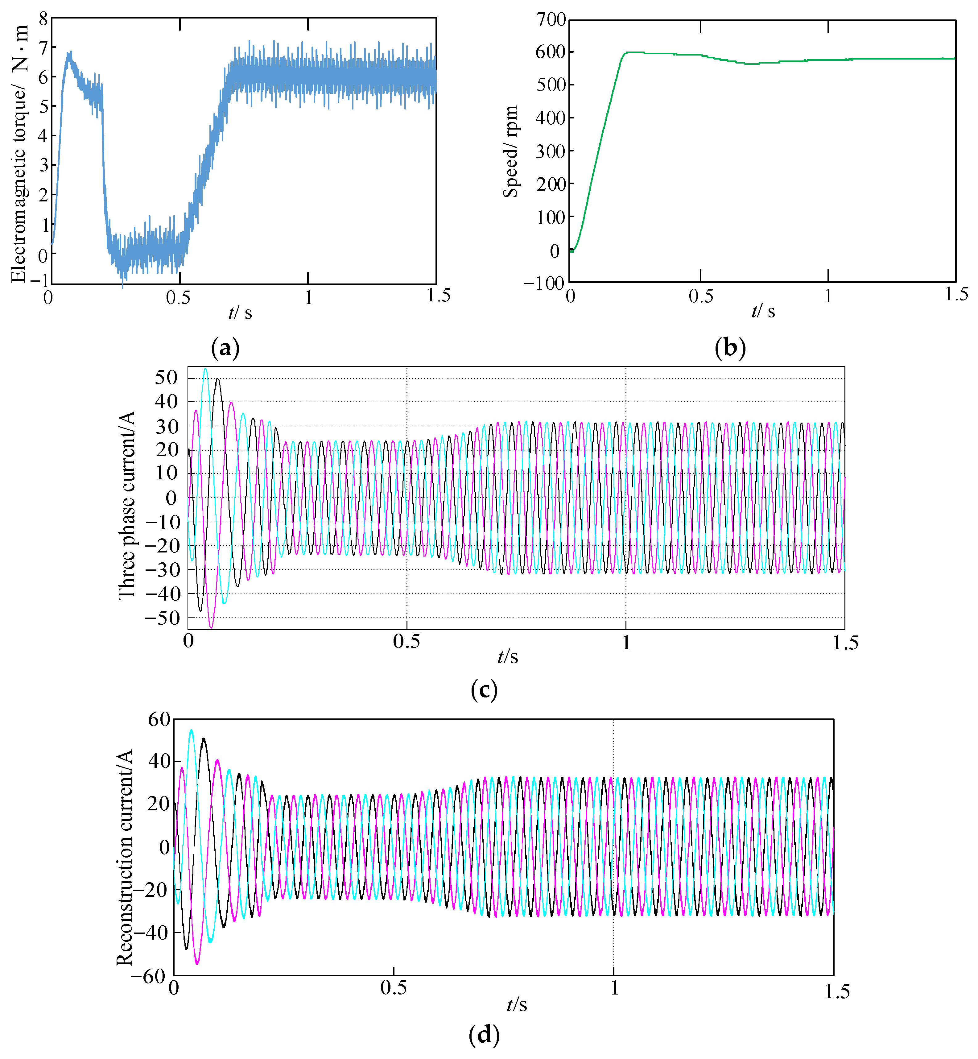
Finally, the closed-loop vector control performances based on DPWM2 were verified, and instead of current detection, the phase current reconstruction method based on the DC-link current sampling method proposed in this paper was used to obtain the stator current. The command value of the speed was set as 600 rpm, and the torque load was set to 6 N·m. The simulation waveforms of the torque, the speed, and the three-phase stator currents are shown in Figure 19. After 0.2 s, the speed reached 600 rpm without steady error. According to Figure 19c,d, the amplitude and the phase of the reconstruction of the three-phase currents are the same as the measured current.

7. Experimental Results

An experimental platform was established and mainly composed of a driver with a controller, DC power supply, IM, a communication system, and a measuring device, which are shown in Figure 20. The control algorithm was executed by using the DSP made in Freescale, whose type is 56F830, and the type of the switching device is IPB042N10N3 made by Infineon. The parameters of the IM adopted in this experiment are shown in Table 3.
Two interrupt programs were included and triggered by A/D and PWM signals: the algorithm of DC-link current sampling was completed by the A/D interrupt program, and the programs of vector control and DPWM2 were completed by the PWM interrupt program.
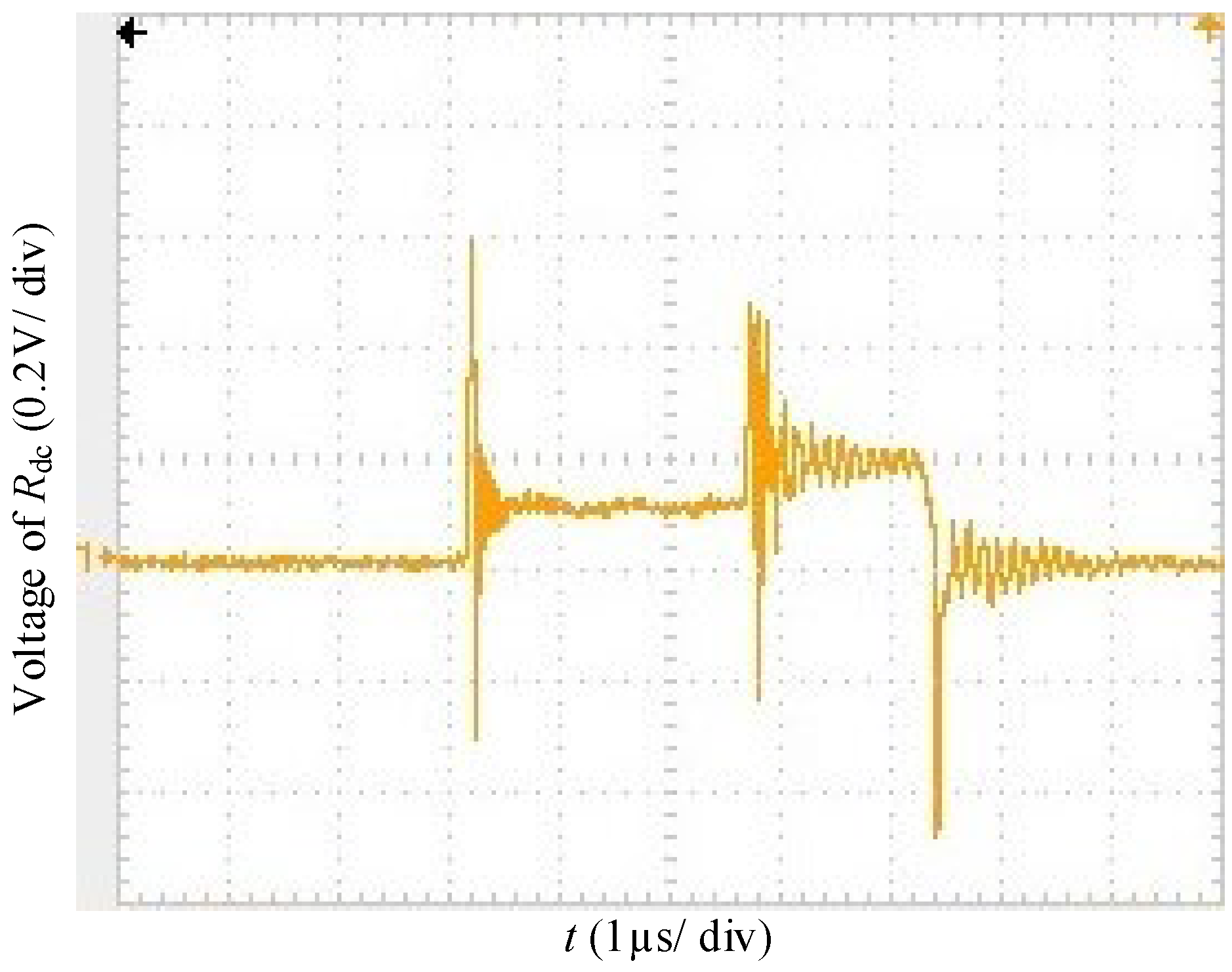
The experimental waveform of the modulation ratio is shown in Figure 21a. The shape is the same as that in Figure 3. The waveform of the switching signal is shown in Figure 21b. In two one-sixth cycles, the switching signal remained at the ON or OFF state, so the correctness of the DPWM2 modulation algorithm designed in this paper was verified. Figure 22 shows the voltage of the DC-link sampling resistor; when the switching state suddenly changed, after about 0.3 µs oscillation, the voltage of Rdc reached a steady state.
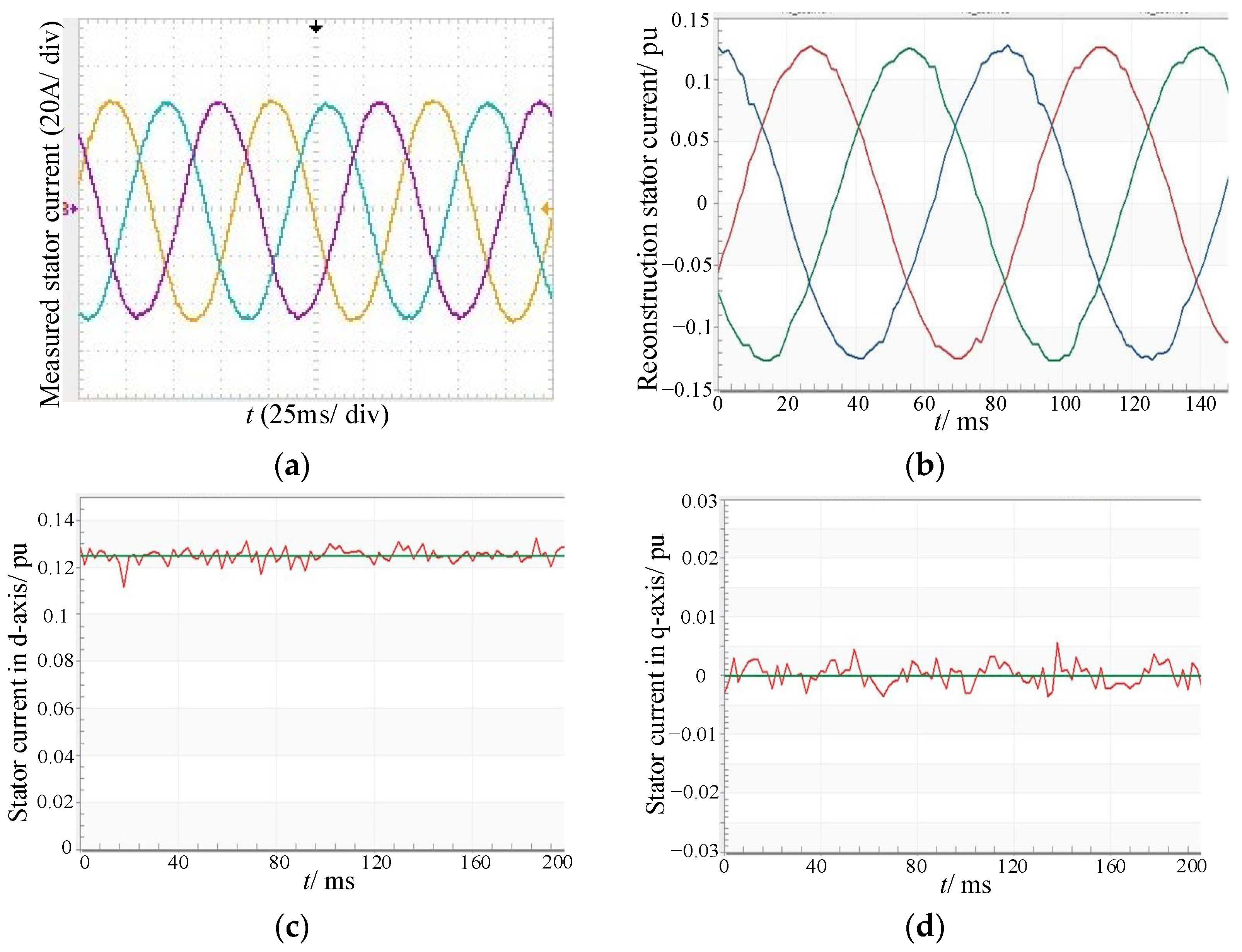
In order to verify the control performance of low modulation area, IM operates without load. The measured stator current is shown in Figure 23a. The current waveform is very smooth without obvious distortion and burrs. The reconstruction stator current is shown in Figure 23b, which indicates that a good reconstruction effect can be obtained. Figure 23c,d show the waveforms of the stator current in the d–q axis, indicating that both ids and iqs can track the command value without a large ripple. The experimental results show the feasibility and correctness of the three-phase current reconstruction method with sampling time compensation for DPWM2.
Under the same operation condition and DPWM2, a quantitative comparison of the proposed method with the vector control based on the current sensor was made, as shown in Table 4. Due to a little reconstruction current error at the sector boundary, the fifth component of the stator current slightly increased, which caused a slight increase in the THD of the stator current and the torque ripple. The cancellation of the current sensor had little impact on the control performance.

8. Conclusions

In order to reduce the cost and the switching loss of the voltage source inverter-fed inductor motor drive system, this paper presented a novel three-phase current reconstruction method based on DC-link current sampling for DPWM2, and a time compensation strategy was proposed to solve the problem that the duration of the active vector is too short to sample DC-link current. The feasibility and correctness were verified through simulations and experimental results. The main contribution could be summarized as follows:
(1)
Three current samples were completed in different switching states during the carrier rise stage, and the mathematical expressions between the three-phase currents and the measured DC-link current in different sectors were derived;
(2)
When the target voltage vector was located near the sector boundary, if the total duration of the active vector was greater than the minimum sampling time, or the half of duration of the first active vector was less than the minimum sampling time, the duration of the active vector in the sampling stage can be broadened by phase shifting without changing the synthetic vector in one carrier period;
(3)
If the half duration of the first active vector was less than the minimum sampling time, or the target voltage vector was located in the low modulation areas, a time compensation method combining phase shifting and frequency reduction was proposed, and the accurate reconstruction of three-phase currents can be realized without voltage vector error.

Author Contributions

Conceptualization and methodology, P.S.; simulation, Y.L.; validation and experiment, P.S. and J.Z.; writing and supervision, T.D. and Y.L.; writing—review and editing, P.S.; funding acquisition, H.W. All authors have read and agreed to the published version of the manuscript.

Funding

This work was supported by “the Fundamental Research Funds for the Central Universities”, Southwest Minzu University (Funder, Huazhang Wang; Funding number, 2021101).

Data Availability Statement

Not applicable.

Conflicts of Interest

The authors declare no conflict of interest regarding the publication of this paper.

References

  1. Rajeev, M.; Agarwal, V. Single phase current source inverter with multiloop control for transformerless grid–PV interface. IEEE Trans. Ind. Appl. 2018, 54, 2416–2424. [Google Scholar] [CrossRef]
  2. Song, P.; Liu, Y.; Liu, C. Research on Parameter Design and Control Method for Current Source Inverter–Fed IM Drive Systems. Machines 2022, 10, 922. [Google Scholar] [CrossRef]
  3. Dong, Z.; Liu, C.; Song, Z.; Liu, S. Suppression of Dual–Harmonic Components for Five–Phase Series–Winding PMSM. IEEE Trans. Transp. Electrif. 2022, 8, 121–134. [Google Scholar] [CrossRef]
  4. Song, Z.; Liu, C.; Dong, Z.; Huang, R. Improved Multi-Stage Decoupling Space Vector Modulation for Asymmetrical Multi-Phase PMSM With Series Winding Connection. IEEE Trans. Power Electron. 2022, 37, 10951–10966. [Google Scholar] [CrossRef]
  5. Arora, S.; Balsara, P.T.; Bhatia, D. Digital Pulsewidth Modulation (DPWM) Using Direct Digital Synthesis. IEEE J. Emerg. Sel. Top. Power Electron. 2022, 10, 4231–4244. [Google Scholar] [CrossRef]
  6. Hashempour, M.M.; Yang, M.-Y.; Lee, T.-L. An Adaptive Control of DPWM for Clamped-Three-Level Photovoltaic Inverters with Unbalanced Neutral-Point Voltage. IEEE Trans. Ind. Appl. 2018, 54, 6133–6148. [Google Scholar] [CrossRef]
  7. Charumit, C.; Kinnares, V. Discontinuous SVPWM Techniques of Three-Leg VSI-Fed Balanced Two-Phase Loads for Reduced Switching Losses and Current Ripple. IEEE Trans. Power Electron. 2015, 30, 2191–2204. [Google Scholar] [CrossRef]
  8. Torres, D.; Zambada, J. Single-Shunt Three-Phase Current Reconstruction Algorithm for Sensorless foc of a Pmsm; Microchip Technology application note AN1299; Microchip Technology Inc.: Chandler, AZ, USA, 2009. [Google Scholar]
  9. Tcai, A.; Shin, H.-U.; Lee, K.-B. DC-Link Capacitor-Current Ripple Reduction in DPWM-Based Back-to-Back Converters. IEEE Trans. Ind. Electron. 2018, 65, 1897–1907. [Google Scholar] [CrossRef]
  10. Yan, H.; Xu, Y.; Zhao, W.; Zhang, H.; Gerada, C. DC Drift Error Mitigation Method for Three-Phase Current Reconstruction With Single Hall Current Sensor. IEEE Trans. Magn. 2019, 55, 1–4. [Google Scholar] [CrossRef]
  11. Song, S.; Xia, Z.; Fang, G.; Ma, R.; Liu, W. Phase Current Reconstruction and Control of Three-Phase Switched Reluctance Machine with Modular Power Converter Using Single DC-Link Current Sensor. IEEE Trans. Power Electron. 2018, 33, 8637–8649. [Google Scholar] [CrossRef]
  12. Han, J.; Song, J.-H. Phase Current-Balance Control Using DC-Link Current Sensor for Multiphase Converters with Discontinuous Current Mode Considered. IEEE Trans. Ind. Electron. 2016, 63, 4020–4030. [Google Scholar] [CrossRef]
  13. Gan, C.; Wu, J.; Yang, S.; Hu, Y. Phase Current Reconstruction of Switched Reluctance Motors From DC-Link Current Under Double High-Frequency Pulses Injection. IEEE Trans. Ind. Electron. 2015, 62, 3265–3276. [Google Scholar] [CrossRef] [Green Version]
  14. Wei, H.; Lu, Y.; Jiang, T.; Li, Y.; Chu, J. Single Resistor Sampling Reconstruction of Permanent Magnet Synchronous Motor Considering Non-Observation Area Compensation. Trans. China Electrotech. Soc. 2018, 33, 2702–2965. [Google Scholar]
  15. Saritha, B.; Janakiraman, P.A. Sinusoidal Three-Phase Current Reconstruction and Control Using a DC-Link Current Sensor and a Curve-Fitting Observer. IEEE Trans. Ind. Electron. 2015, 54, 2657–2664. [Google Scholar] [CrossRef]
  16. Cho, Y.; LaBella, T.; Lai, J.-S. A Three-Phase Current Reconstruction Strategy with Online Current Offset Compensation Using a Single Current Sensor. IEEE Trans. Ind. Electron. 2012, 59, 2924–2933. [Google Scholar] [CrossRef]
  17. Hongrae, K.; Jahns, T.M. Phase Current Reconstruction for AC Motor Drives Using a DC Link Single Current Sensor and Measurement Voltage Vectors. IEEE Trans. Power Electron. 2006, 21, 1413–1419. [Google Scholar]
  18. Han, G.; Chen, H.; Shi, X.; Wang, Y. Phase current reconstruction strategy for switched reluctance machines with fault-tolerant capability. IET Elect. Power Appl. 2017, 11, 399–411. [Google Scholar] [CrossRef]
  19. Yikun, G.; Fenglei, N.; Dapeng, Y.; Hong, L. Switching-State Phase Shift Method for Three-Phase-Current Reconstruction With a Single DC-Link Current Sensor. IEEE Trans. Ind. Electron. 2006, 58, 5186–5194. [Google Scholar] [CrossRef]
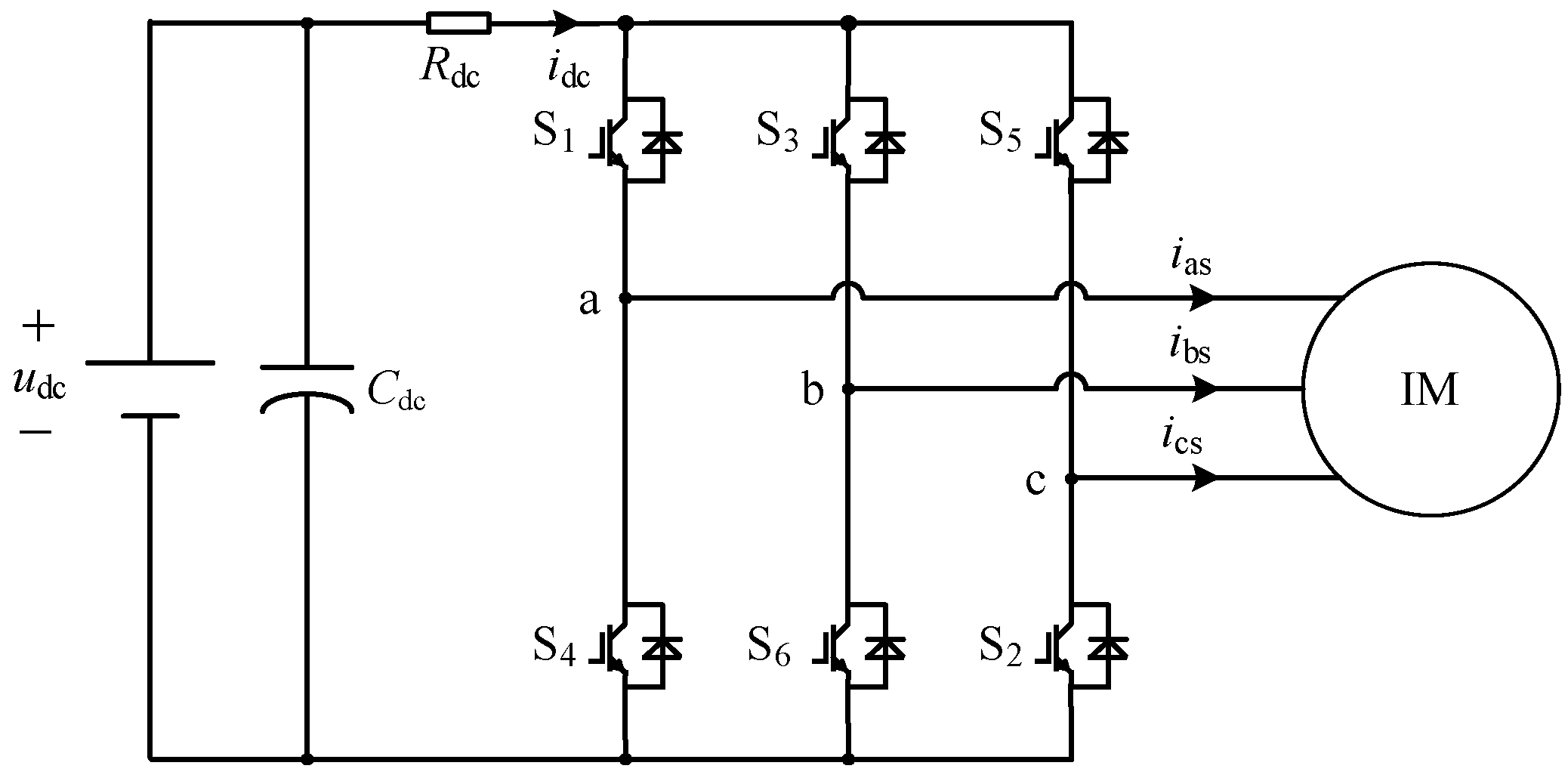
Figure 1. The topology of VSI-fed IM drive system.
Machines 10 01104 g001
Figure 2. Block diagram of the vector control scheme.
Machines 10 01104 g002
Figure 3. Waveforms of the modulation ratio of phases a, b, and c in a carrier period.
Machines 10 01104 g003
Figure 4. Switching sequences of DPWM2 in different sectors during one carrier period: (a) Sector I; (b) Sector II; (c) Sector III; (d) Sector IV; (e) Sector V; (f) Sector VI.
Machines 10 01104 g004aMachines 10 01104 g004b
Figure 5. Equivalent circuits under different switching states: (a) 100; (b) 110; (c) 010; (d) 011; (e) 001; (f) 101; (g) 111; (h) 000.
Machines 10 01104 g005
Figure 6. The diagrams of the three-phase current reconstruction of DPWM2 based on the DC-link current sampling: (a) Sector I; (b) Sector II.
Machines 10 01104 g006
Figure 7. The vector diagram.
Machines 10 01104 g007
Figure 8. The areas near the sector boundary in Sectors I and II.
Machines 10 01104 g008
Figure 9. The diagram of the phase-shifting compensation method in Sector I when T2  (Tmin, 2Tmin): (a) before phase shifting; (b) after phase shifting.
Machines 10 01104 g009
Figure 10. The diagram of the phase-shifting compensation method in Sector I when T2 < Tmin: (a) before phase shifting; (b) after phase shifting.
Machines 10 01104 g010
Figure 11. The diagram of the phase-shifting compensation method in Sector I when T1  (Tmin, 2Tmin): (a) before phase shifting; (b) after phase shifting.
Machines 10 01104 g011
Figure 12. Diagram of phase shifting and frequency reduction in Sector I when T1 < Tmin.
Machines 10 01104 g012
Figure 13. The diagram of the phase-shifting compensation method in Sector II when T3 < Tmin: (a) before phase shifting; (b) after phase shifting.
Machines 10 01104 g013
Figure 14. The diagram of the phase-shifting compensation method in region 4 when T2 < Tmin: (a) before phase shifting; (b) after phase shifting.
Machines 10 01104 g014
Figure 15. The diagram of the switching state when V ref is located in the area of low modulation belonging to Sector I.
Machines 10 01104 g015
Figure 16. The diagram of the switching state when V ref is located in the area of low modulation belonging to Sector II.
Machines 10 01104 g016
Figure 17. The simulation model in MATLAB.
Machines 10 01104 g017
Figure 18. The simulation waveforms of three-phase currents: (a) real current; (b) construction current without time compensation; (c) construction current with time compensation.
Machines 10 01104 g018aMachines 10 01104 g018b
Figure 19. The simulation waveforms of closed-loop vector control: (a) electromagnetic torque; (b) speed; (c) measured current; (d) construction current.
Machines 10 01104 g019
Figure 20. Prototype for VSI-fed IM drive system.
Machines 10 01104 g020
Figure 21. The experimental waveforms of DPWM2: (a) modulation ratio; (b) switching signal.
Machines 10 01104 g021
Figure 22. The experimental waveform of the voltage of the sampling resistor in DC-link.
Machines 10 01104 g022
Figure 23. Experimental waveforms without load: (a) measured current; (b) reconstruction current; (c) ids; (d) iqs.
Machines 10 01104 g023
Table 1. The modulation ratio function of DPWM2.
Sectorθmambmc
I0≤ θ < π/311 − 3 Mcos(θ + π/6)1 + 3 Mcos(θ + 5π/6)
IIπ/3 ≤ θ < 2π/3−1 − 3 Mcos(θ + 5π/6)−1 + 3 Msin(θ)−1
III2π/3 ≤ θ < π1 + 3 Mcos(θ + π/6)11 − 3 Msin(θ)
IV−π ≤ θ < −2π/3−1−1 − 3 Mcos(θ + π/6)−1 + 3 Mcos(θ + 5π/6)
V−2π/3 ≤ θ < −π/31 − 3 Mcos(θ + 5π/6)1 + 3 Msin(θ)1
VI−π/3 ≤ θ < 0−1 + 3 Mcos(θ + π/6)−1−1 − 3 Msin(θ)
Table 2. The relationship between DC-link current and the three-phase currents.
Switching-State000100110010011001101111
idc0iasicsibsiasicsibs0
Table 3. The parameters of the IM for the experiment.
ParametersDescriptionValue
Rs (Ω)Stator resistance0.07
Rr (Ω)Rotor resistance0.05
Ls (mH)Stator inductance4.51
Lr (mH)Rotor inductance4.63
Lm (mH)Mutual inductance4.38
σFlux leakage coefficient0.088
Pn (kW)Rated power1.2
Un (V)Rated voltage48
fn (Hz)Rated frequency50
J (kg·m2)Rotational inertia0.001
npNumber of pole pairs2
Table 4. Quantitative comparison between the proposed method and the current sensor sampling.
Current Acquisition MethodSteady ErrorTHD of Stator Current5th HarmonicTorque Ripple (N·m)
ReconstructionNo4.65%1.21%±0.50
Hall sensorsNo4.09%0.95%±0.36
Publisher’s Note: MDPI stays neutral with regard to jurisdictional claims in published maps and institutional affiliations.