Inkjet Etching of Polymers and Its Applications in Organic Electronic Devices


Abstract
:1. Introduction
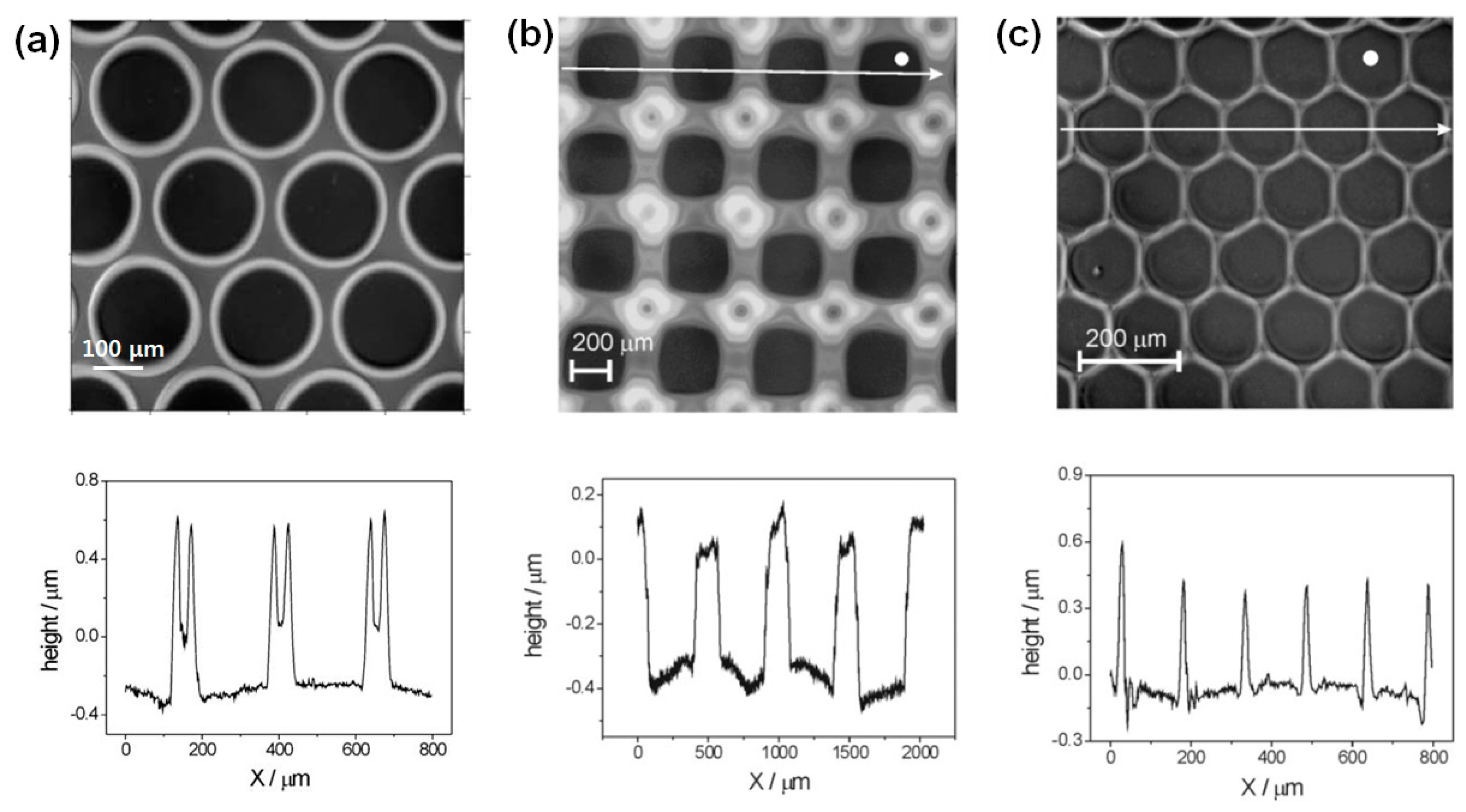
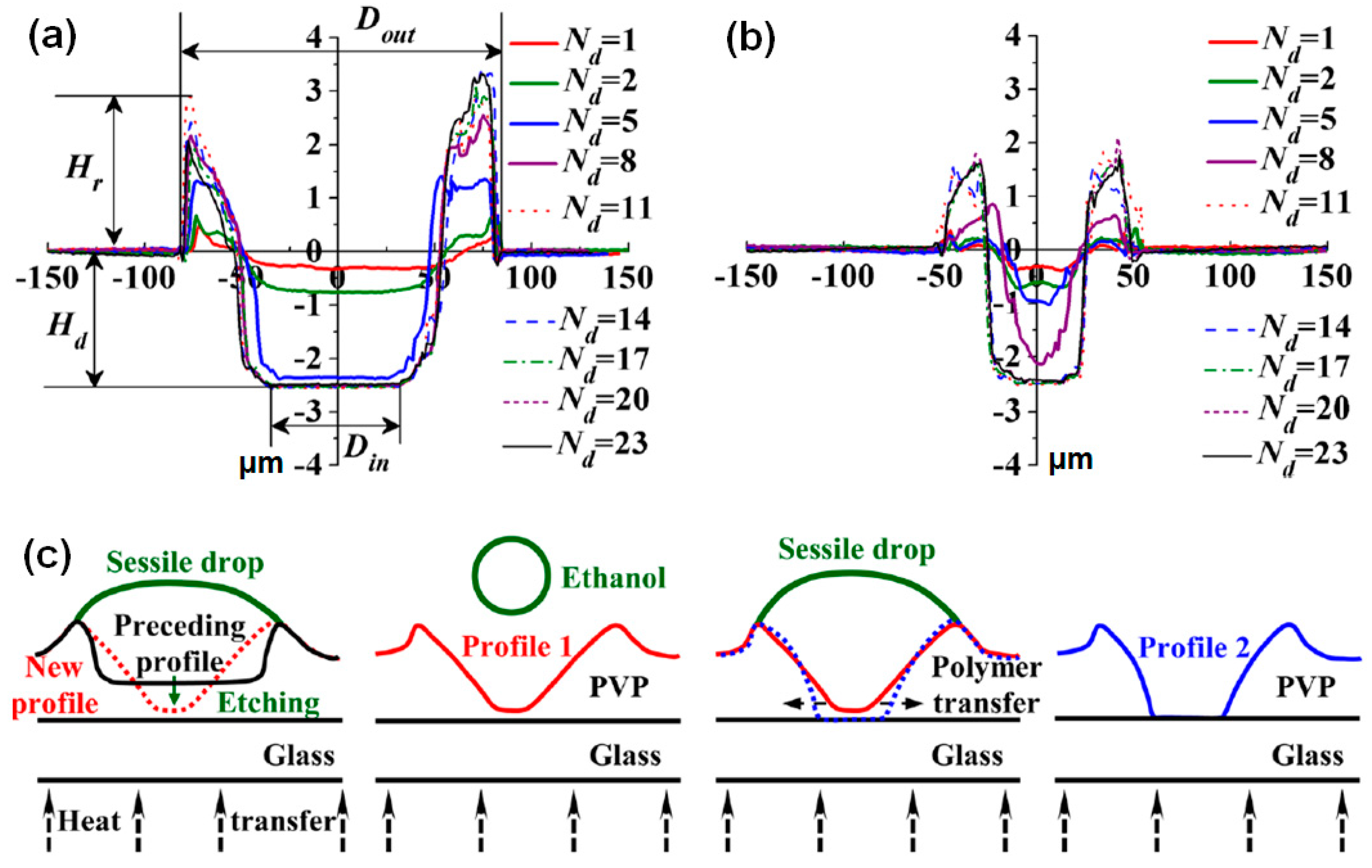
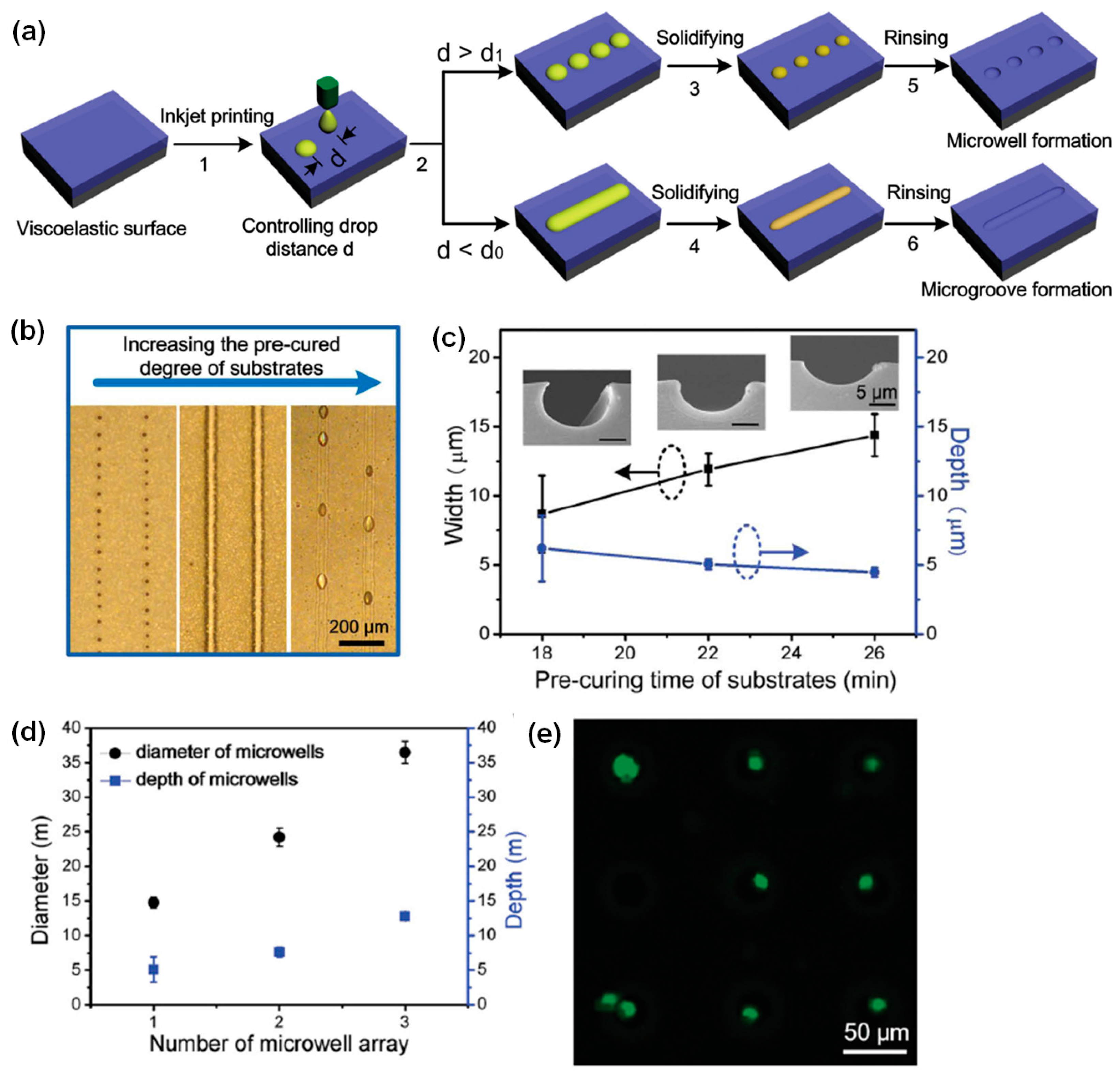
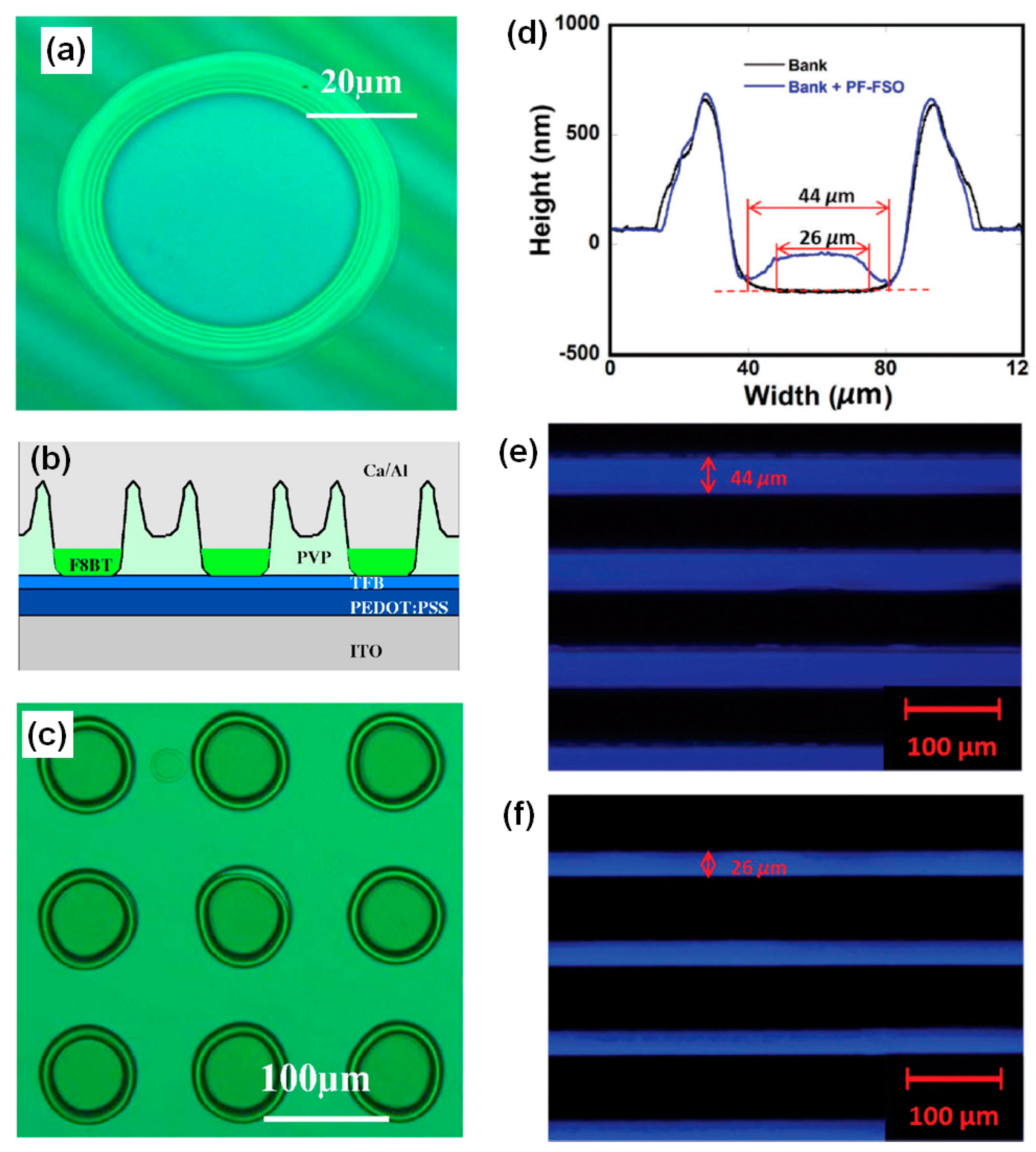
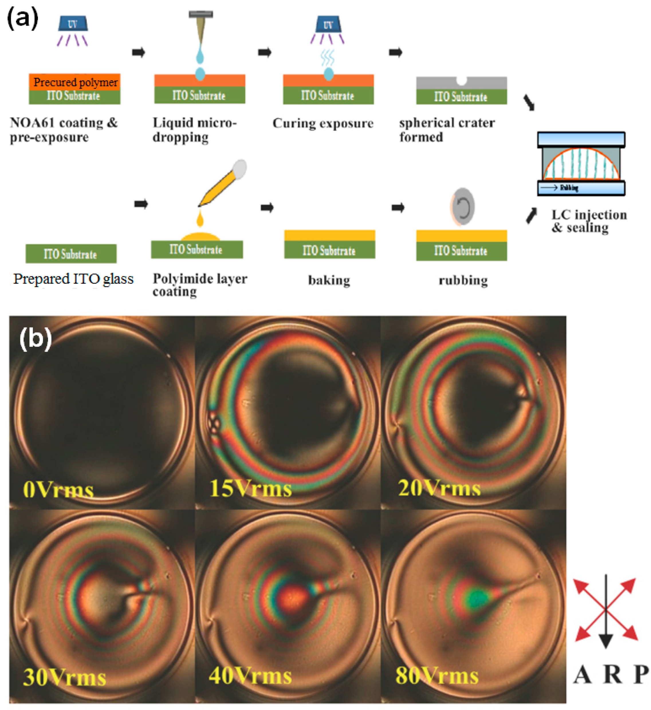
2. Inkjet Etching of Polymers
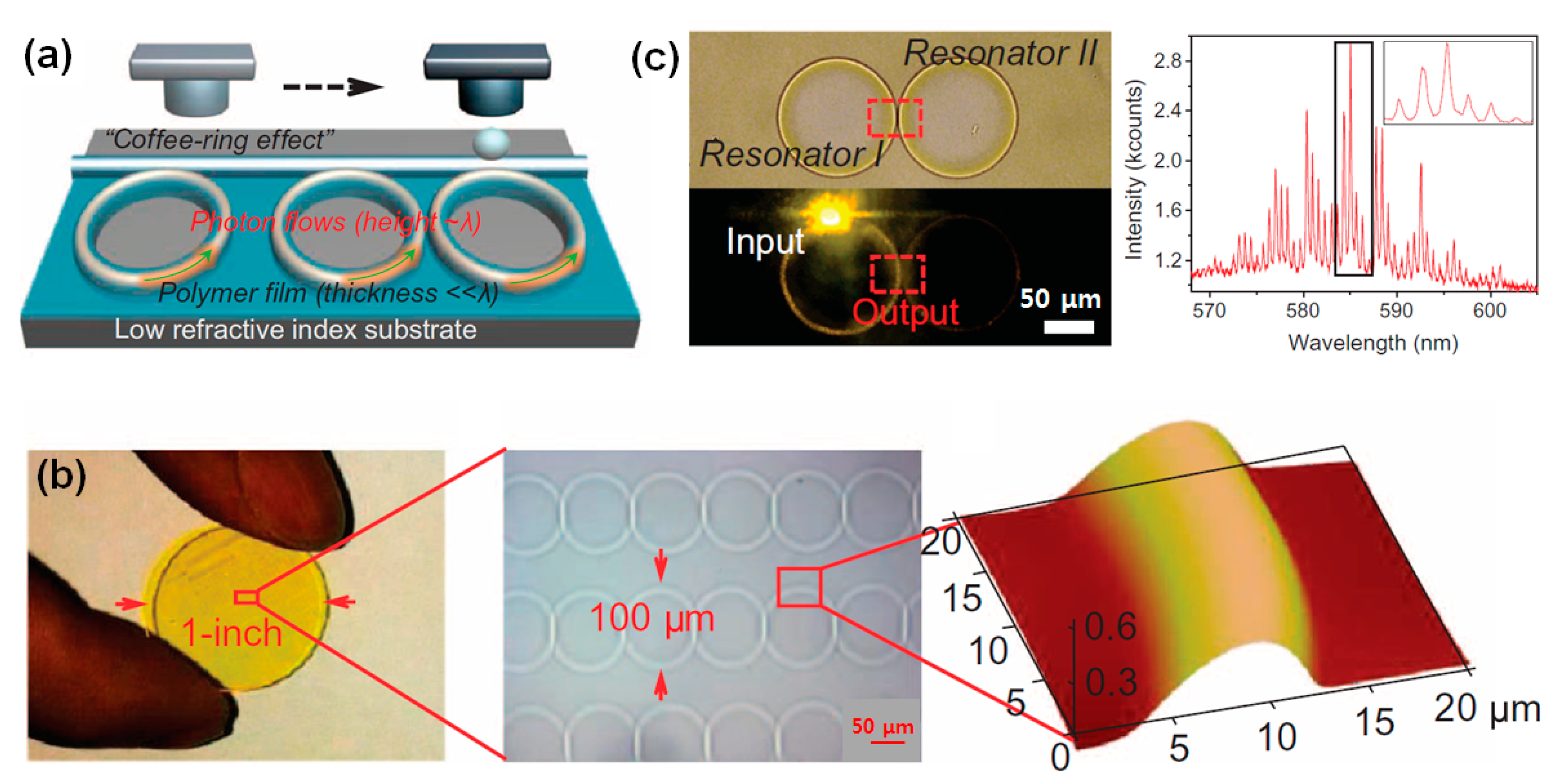
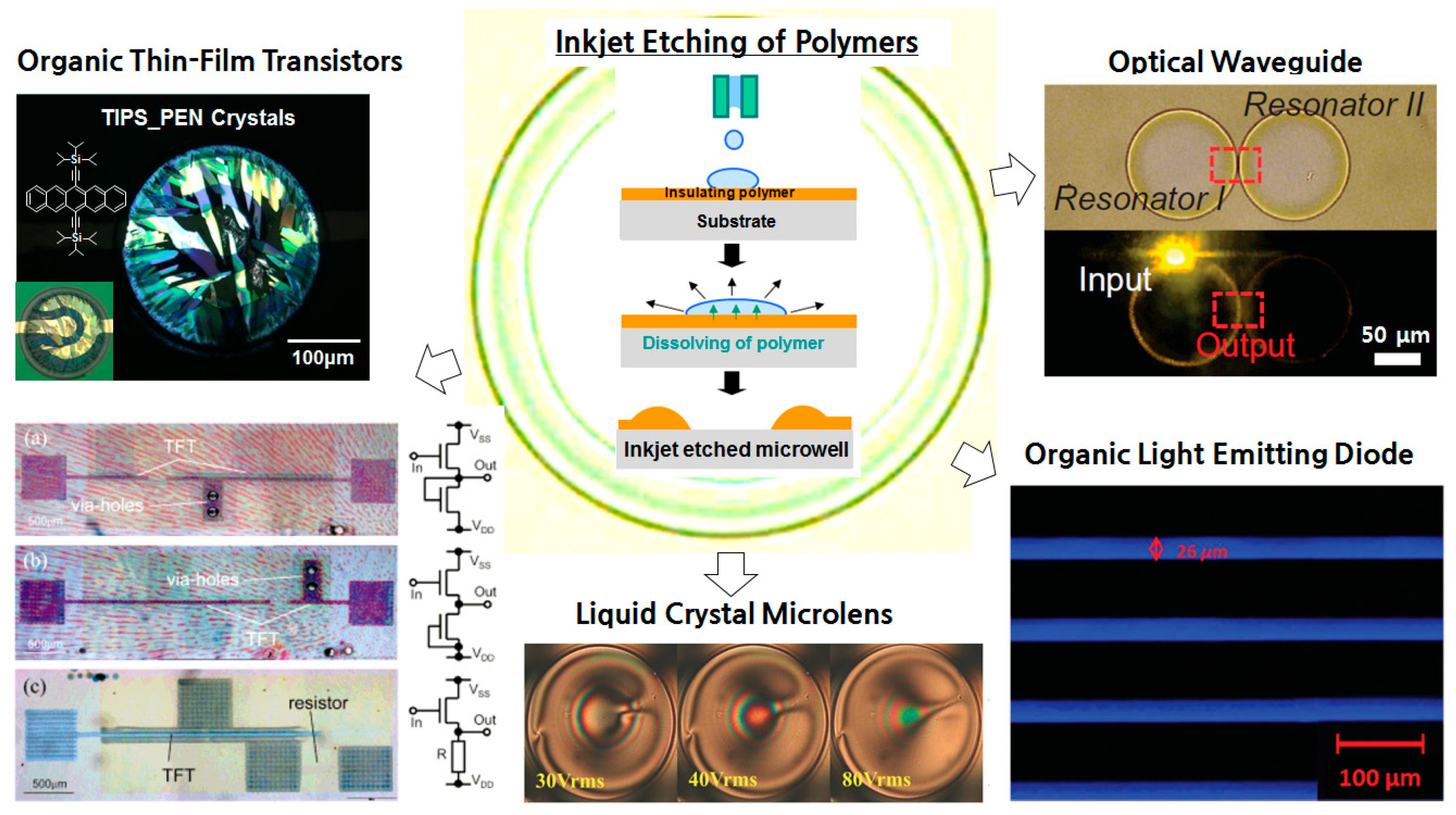
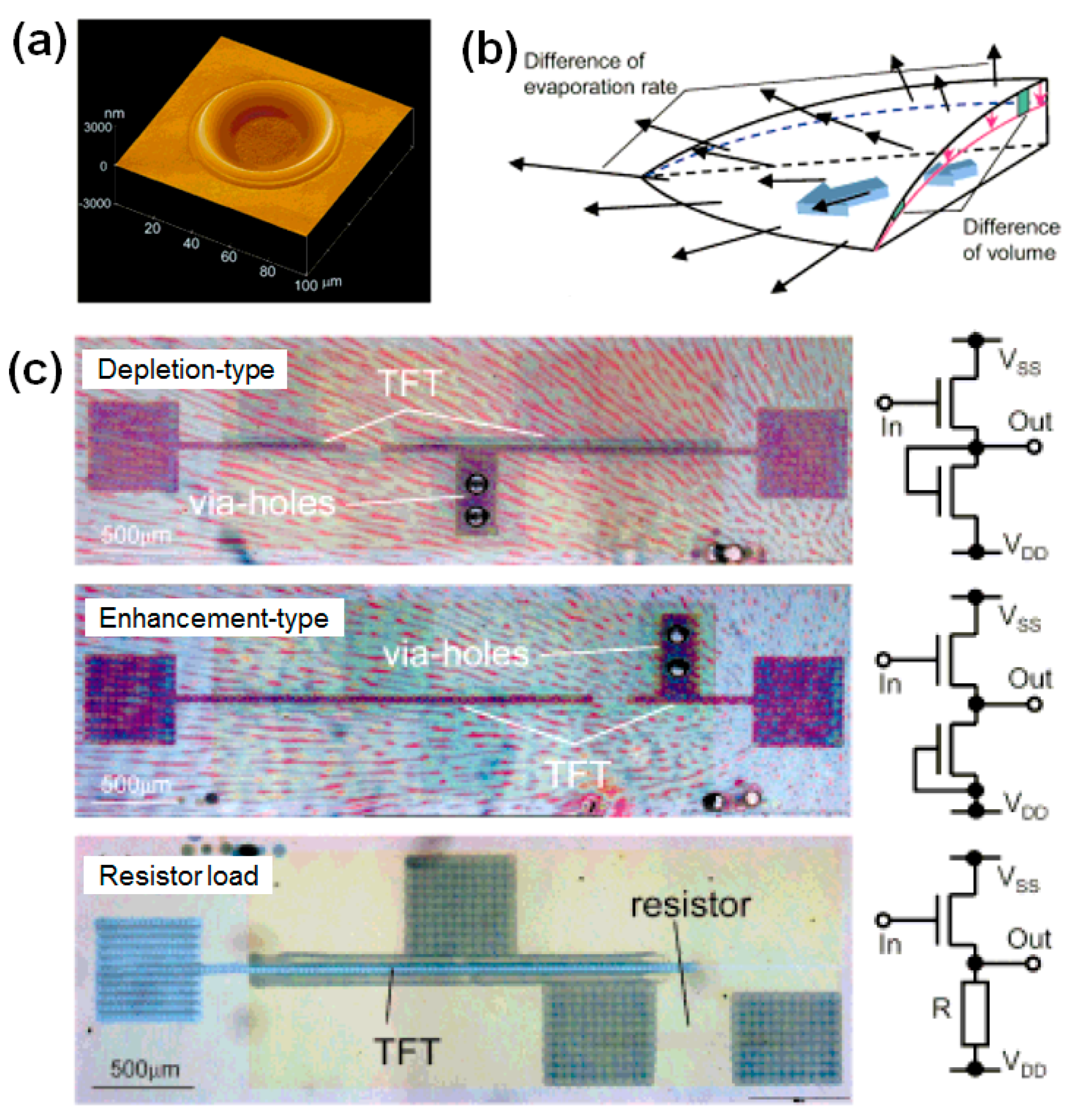
3. Applications in Organic Electronic Devices
4. Conclusions and Outlook
Acknowledgments
Author Contributions
Conflicts of Interest
References
- Calvert, P. Inkjet printing for materials and devices. Chem. Mater. 2001, 13, 3299–3305. [Google Scholar] [CrossRef]
- De Gans, B.J.; Duineveld, P.C.; Schubert, U.S. Inkjet printing of polymers: State of the art and future developments. Adv. Mater. 2004, 16, 203–213. [Google Scholar] [CrossRef]
- Singh, M.; Haverinen, H.M.; Dhagat, P.; Jabbour, G.E. Inkjet printing-process and its applications. Adv. Mater. 2010, 22, 673–685. [Google Scholar] [CrossRef] [PubMed]
- Belgardt, C.; Sowade, E.; Blaudeck, T.; Baumgartel, T.; Graaf, H.; von Borczyskowski, C.; Baumann, R.R. Inkjet printing as a tool for the patterned deposition of octadecylsiloxane monolayers on silicon oxide surfaces. Phys. Chem. Chem. Phys. 2013, 15, 7494–7504. [Google Scholar] [CrossRef] [PubMed]
- Tekin, E.; Smith, P.J.; Schubert, U.S. Inkjet printing as a deposition and patterning tool for polymers and inorganic particles. Soft Matter 2008, 4, 703–713. [Google Scholar] [CrossRef]
- Yamada, K.; Henares, T.G.; Suzuki, K.; Citterio, D. Paper-based inkjet-printed microfluidic analytical devices. Angew. Chem. Int. Ed. 2015, 54, 5294–5310. [Google Scholar] [CrossRef] [PubMed]
- Tao, H.; Marelli, B.; Yang, M.M.; An, B.; Onses, M.S.; Rogers, J.A.; Kaplan, D.L.; Omenetto, F.G. Inkjet printing of regenerated silk fibroin: From printable forms to printable functions. Adv. Mater. 2015, 27, 4273–4279. [Google Scholar] [CrossRef] [PubMed]
- Teichler, A.; Perelaer, J.; Schubert, U.S. Inkjet printing of organic electronics-comparison of deposition techniques and state-of-the-art developments. J. Mater. Chem. C 2013, 1, 1910–1925. [Google Scholar] [CrossRef]
- Kwon, J.; Takeda, Y.; Fukuda, K.; Cho, K.; Tokito, S.; Jung, S. Three-dimensional, inkjet-printed organic transistors and integrated circuits with 100% yield, high uniformity, and long-term stability. ACS Nano 2016, 10, 10324–10330. [Google Scholar] [CrossRef] [PubMed]
- Kwon, Y.J.; Park, Y.D.; Lee, W.H. Inkjet-printed organic transistors based on organic semiconductor/insulating polymer blends. Materials 2016, 9, 650–665. [Google Scholar] [CrossRef] [PubMed]
- Kawase, T.; Sirringhaus, H.; Friend, R.H.; Shimoda, T. Inkjet printed via-hole interconnections and resistors for all-polymer transistor circuits. Adv. Mater. 2001, 13, 1601–1605. [Google Scholar] [CrossRef]
- Cho, S.Y.; Ko, J.M.; Lim, J.; Lee, J.Y.; Lee, C. Inkjet-printed organic thin film transistors based on tips pentacene with insulating polymers. J. Mater. Chem. C 2013, 1, 914–923. [Google Scholar] [CrossRef]
- James, D.T.; Kjellander, B.K.C.; Smaal, W.T.T.; Gelinck, G.H.; Combe, C.; McCulloch, I.; Wilson, R.; Burroughes, J.H.; Bradley, D.D.C.; Kim, J.S. Thin-film morphology of inkjet-printed single-droplet organic transistors using polarized raman spectroscopy: Effect of blending tips-pentacene with insulating polymer. Acs Nano 2011, 5, 9824–9835. [Google Scholar] [CrossRef] [PubMed]
- Kang, B.; Lee, W.H.; Cho, K. Recent advances in organic transistor printing processes. ACS Appl. Mater. Interfaces 2013, 5, 2302–2315. [Google Scholar] [CrossRef] [PubMed]
- Kjellander, B.K.C.; Smaal, W.T.T.; Anthony, J.E.; Gelinck, G.H. Inkjet printing of tips-pen on soluble polymer insulating films: A route to high-performance thin-film transistors. Adv. Mater. 2010, 22, 4612–4616. [Google Scholar] [CrossRef] [PubMed]
- Kwak, D.; Choi, H.H.; Kang, B.; Kim, D.H.; Lee, W.H.; Cho, K. Tailoring morphology and structure of inkjet-printed liquid-crystalline semiconductor/insulating polymer blends for high-stability organic transistors. Adv. Funct. Mater. 2016. [Google Scholar] [CrossRef]
- Lim, J.A.; Kim, J.H.; Qiu, L.; Lee, W.H.; Lee, H.S.; Kwak, D.; Cho, K. Inkjet-printed single-droplet organic transistors based on semiconductor nanowires embedded in insulating polymers. Adv. Funct. Mater. 2010, 20, 3292–3297. [Google Scholar] [CrossRef]
- Madec, M.B.; Smith, P.J.; Malandraki, A.; Wang, N.; Korvink, J.G.; Yeates, S.G. Enhanced reproducibility of inkjet printed organic thin film transistors based on solution processable polymer-small molecule blends. J. Mater. Chem. 2010, 20, 9155–9160. [Google Scholar] [CrossRef]
- Xia, Y.J.; Friend, R.H. Nonlithographic patterning through inkjet printing via holes. Appl Phys. Lett. 2007, 90, 253513–253515. [Google Scholar] [CrossRef]
- Wu, L.; Dong, Z.C.; Li, F.Y.; Zhou, H.H.; Song, Y.L. Emerging progress of inkjet technology in printing optical materials. Adv. Opt. Mater. 2016, 4, 1915–1932. [Google Scholar] [CrossRef]
- Li, J.T.; Ye, F.; Vaziri, S.; Muhammed, M.; Lemme, M.C.; Ostling, M. Efficient inkjet printing of graphene. Adv. Mater. 2013, 25, 3985–3992. [Google Scholar] [CrossRef] [PubMed]
- Kim, D.; Lee, S.H.; Jeong, S.; Moon, J. All-ink-jet printed flexible organic thin-film transistors on plastic substrates. Electrochem. Solid State Lett. 2009, 12, 195–197. [Google Scholar] [CrossRef]
- Alaman, J.; Alicante, R.; Pena, J.I.; Sanchez-Somolinos, C. Inkjet printing of functional materials for optical and photonic applications. Materials 2016, 9, 910–956. [Google Scholar] [CrossRef] [PubMed]
- Lee, W.H.; Park, Y.D. Organic semiconductor/insulator polymer blends for high-performance organic transistors. Polymers 2014, 6, 1057–1073. [Google Scholar] [CrossRef]
- Lim, S.; Kang, B.; Kwak, D.; Lee, W.H.; Lim, J.A.; Cho, K. Inkjet-printed reduced graphene oxide/poly(vinyl alcohol) composite electrodes for flexible transparent organic field-effect transistors. J. Phys. Chem. C 2012, 116, 7520–7525. [Google Scholar] [CrossRef]
- Jahn, S.F.; Engisch, L.; Baumann, R.R.; Ebert, S.; Goedel, W.A. Polymer microsieves manufactured by inkjet technology. Langmuir 2009, 25, 606–610. [Google Scholar] [CrossRef] [PubMed]
- Zhang, X.H.; Wei, X.X.; Ducker, W. Formation of nanodents by deposition of nanodroplets at the polymer-liquid interface. Langmuir 2010, 26, 4776–4781. [Google Scholar] [CrossRef] [PubMed]
- Kwak, D.; Lim, J.A.; Kang, B.; Lee, W.H.; Cho, K. Self-organization of inkjet-printed organic semiconductor films prepared in inkjet-etched microwells. Adv. Funct. Mater. 2013, 23, 5224–5231. [Google Scholar] [CrossRef]
- Hwang, S.J.; Liu, Y.X.; Porter, G.A. Tunable liquid crystal microlenses with crater polymer prepared by droplet evaporation. Opt. Express 2013, 21, 30731–30738. [Google Scholar] [CrossRef] [PubMed]
- Zhang, C.; Zou, C.L.; Zhao, Y.; Dong, C.H.; Wei, C.; Wang, H.; Liu, Y.; Guo, G.C.; Yao, J.; Zhao, Y.S. Organic printed photonics: From microring lasers to integrated circuits. Sci. Adv. 2015. [Google Scholar] [CrossRef] [PubMed]
- Wang, J.H.; Song, C.; Zhong, Z.M.; Hu, Z.H.; Han, S.H.; Xu, W.; Peng, J.B.A.; Ying, L.; Wang, J.; Cao, Y. In situ patterning of microgrooves via inkjet etching for a solution-processed oled display. J. Mater. Chem. C 2017, 5, 5005–5009. [Google Scholar] [CrossRef]
- De Gans, B.J.; Hoeppener, S.; Schubert, U.S. Polymer-relief microstructures by inkjet etching. Adv. Mater. 2006, 18, 910–914. [Google Scholar] [CrossRef]
- De Gans, B.J.; Hoeppener, S.; Schubert, U.S. Polymer relief microstructures by inkjet etching. J. Mater. Chem. 2007, 17, 3045–3050. [Google Scholar] [CrossRef]
- Robin, M.; Kuai, W.L.; Amela-Cortes, M.; Cordier, S.; Molard, Y.; Mohammed-Brahim, T.; Jacques, E.; Harnois, M. Epoxy based ink as versatile material for inkjet-printed devices. ACS Appl. Mater. Interfaces 2015, 7, 21975–21984. [Google Scholar] [CrossRef] [PubMed]
- Nallan, H.C.; Sadie, J.A.; Kitsomboonloha, R.; Volkman, S.K.; Subramanian, V. Systematic design of jettable nanoparticle-based inkjet inks: Rheology, acoustics, and jettability. Langmuir 2014, 30, 13470–13477. [Google Scholar] [CrossRef] [PubMed]
- Jang, D.; Kim, D.; Moon, J. Influence of fluid physical properties on ink-jet printability. Langmuir 2009, 25, 2629–2635. [Google Scholar] [CrossRef] [PubMed]
- Kim, E.; Baek, J. Numerical study on the effects of non-dimensional parameters on drop-on-demand droplet formation dynamics and printability range in the up-scaled model. Phys. Fluids 2012. [Google Scholar] [CrossRef]
- Pericet-Camara, R.; Bonaccurso, E.; Graf, K. Microstructuring of polystyrene surfaces with nonsolvent sessile droplets. Chem. Phys. Chem. 2008, 9, 1738–1746. [Google Scholar] [CrossRef] [PubMed]
- Zhang, Y.; Liu, C.; Whalley, D.C. The penetration limit of poly(4-vinyl phenol) thin films for etching via holes by inkjet printing. Appl. Phys. Lett. 2012, 101, 253302–253304. [Google Scholar]
- Zhang, Y.; Liu, C.; Whalley, D.C. The impact of substrate temperature on the size and aspect ratio of inkjet-dissolved via holes in thin poly(4-vinyl phenol) dielectric layers. Appl. Phys. Lett. 2013, 102, 103303–103305. [Google Scholar]
- Driscoll, M.; Delmotte, B.; Youssef, M.; Sacanna, S.; Donev, A.; Chaikin, P. Unstable fronts and motile structures formed by microrollers. Nat. Phys. 2017, 13, 375–379. [Google Scholar] [CrossRef]
- Nagatsu, Y.; Ishii, Y.; Tada, Y.; De Wit, A. Hydrodynamic fingering instability induced by a precipitation reaction. Phys. Rev. Lett. 2014. [Google Scholar] [CrossRef] [PubMed]
- Grimaldi, I.A.; Del Mauro, A.D.; Nenna, G.; Loffredo, F.; Minarini, C.; Villani, F. Microstructuring of polymer films by inkjet etching. J. Appl. Polym. Sci. 2011, 122, 3637–3643. [Google Scholar] [CrossRef]
- Bao, B.; Jiang, J.K.; Li, F.Y.; Zhang, P.C.; Chen, S.R.; Yang, Q.; Wang, S.T.; Su, B.; Jiang, L.; Song, Y.L. Fabrication of patterned concave microstructures by inkjet imprinting. Adv. Funct. Mater. 2015, 25, 3286–3294. [Google Scholar] [CrossRef]
- Lee, J.N.; Park, C.; Whitesides, G.M. Solvent compatibility of poly(dimethylsiloxane)-based microfluidic devices. Anal. Chem. 2003, 75, 6544–6554. [Google Scholar] [CrossRef] [PubMed]
- Lee, W.H.; Suk, J.W.; Lee, J.; Hao, Y.F.; Park, J.; Yang, J.W.; Ha, H.W.; Murali, S.; Chou, H.; Akinwande, D.; et al. Simultaneous transfer and doping of cvd-grown graphene by fluoropolymer for transparent conductive films on plastic. ACS Nano 2012, 6, 1284–1290. [Google Scholar] [CrossRef] [PubMed]
- Khim, D.; Baeg, K.J.; Kang, M.; Lee, S.H.; Kim, N.K.; Kim, J.; Lee, G.W.; Liu, C.; Kim, D.Y.; Noh, Y.Y. Inkjet-printing-based soft-etching technique for high-speed polymer ambipolar integrated circuits. ACS Appl. Mater. Interfaces 2013, 5, 12579–12586. [Google Scholar] [CrossRef] [PubMed]
- Giri, G.; Verploegen, E.; Mannsfeld, S.C.B.; Atahan-Evrenk, S.; Kim, D.H.; Lee, S.Y.; Becerril, H.A.; Aspuru-Guzik, A.; Toney, M.F.; Bao, Z.A. Tuning charge transport in solution-sheared organic semiconductors using lattice strain. Nature 2011, 480, 504–508. [Google Scholar] [CrossRef] [PubMed] [Green Version]
- Anthony, J.E.; Brooks, J.S.; Eaton, D.L.; Parkin, S.R. Functionalized pentacene: Improved electronic properties from control of solid-state order. J. Am. Chem. Soc. 2001, 123, 9482–9483. [Google Scholar] [CrossRef] [PubMed]
- Lee, W.H.; Kim, D.H.; Jang, Y.; Cho, J.H.; Hwang, M.; Park, Y.D.; Kim, Y.H.; Han, J.I.; Cho, K. Solution-processable pentacene microcrystal arrays for high performance organic field-effect transistors. Appl. Phys. Lett. 2007, 90, 132106–132108. [Google Scholar] [CrossRef]
- Lee, W.H.; Min, H.; Park, N.; Lee, J.; Seo, E.; Kang, B.; Cho, K.; Lee, H.S. Microstructural control over soluble pentacene deposited by capillary pen printing for organic electronics. ACS Appl. Mater. Interfaces 2013, 5, 7838–7844. [Google Scholar] [CrossRef] [PubMed]
- Lim, J.A.; Lee, H.S.; Lee, W.H.; Cho, K. Control of the morphology and structural development of solution-processed functionalized acenes for high-performance organic transistors. Adv. Funct. Mater. 2009, 19, 1515–1525. [Google Scholar] [CrossRef]
- Lim, J.A.; Lee, W.H.; Kwak, D.; Cho, K. Evaporation-induced self-organization of inkjet-printed organic semiconductors on surface-modified dielectrics for high-performance organic transistors. Langmuir 2009, 25, 5404–5410. [Google Scholar] [CrossRef] [PubMed]
- Lim, J.A.; Lee, W.H.; Lee, H.S.; Lee, J.H.; Park, Y.D.; Cho, K. Self-organization of ink-jet-printed triisopropylsilylethynyl pentacene via evaporation-induced flows in a drying droplet. Adv. Funct. Mater. 2008, 18, 229–234. [Google Scholar] [CrossRef]
- Sekitani, T.; Noguchi, Y.; Zschieschang, U.; Klauk, H.; Someya, T. Organic transistors manufactured using inkjet technology with subfemtoliter accuracy. Proc. Natl. Acad. Sci. USA 2008, 105, 4976–4980. [Google Scholar] [CrossRef] [PubMed]
- Sele, C.W.; von Werne, T.; Friend, R.H.; Sirringhaus, H. Lithography-free, self-aligned inkjet printing with sub-hundred-nanometer resolution. Adv. Mater. 2005, 17, 997–1001. [Google Scholar] [CrossRef]


© 2017 by the authors. Licensee MDPI, Basel, Switzerland. This article is an open access article distributed under the terms and conditions of the Creative Commons Attribution (CC BY) license (http://creativecommons.org/licenses/by/4.0/).
Share and Cite
Lee, W.H.; Park, Y.D. Inkjet Etching of Polymers and Its Applications in Organic Electronic Devices. Polymers 2017, 9, 441. https://doi.org/10.3390/polym9090441
Lee WH, Park YD. Inkjet Etching of Polymers and Its Applications in Organic Electronic Devices. Polymers. 2017; 9(9):441. https://doi.org/10.3390/polym9090441
Chicago/Turabian StyleLee, Wi Hyoung, and Yeong Don Park. 2017. "Inkjet Etching of Polymers and Its Applications in Organic Electronic Devices" Polymers 9, no. 9: 441. https://doi.org/10.3390/polym9090441
APA StyleLee, W. H., & Park, Y. D. (2017). Inkjet Etching of Polymers and Its Applications in Organic Electronic Devices. Polymers, 9(9), 441. https://doi.org/10.3390/polym9090441