Recent Advances of Plasmonic Organic Solar Cells: Photophysical Investigations


Abstract
1. Introduction
2. Mechanism of Plasmonic Enhancement Effect in Opvs
2.1. Far-Field Scattering Effect
2.2. Near-Field Localized and Propagating Plasmonic Effects
2.2.1. Localized Surface Plasmon Resonance (Lspr)
2.2.2. Propagating Surface Plasmon Polariton (Spp)
2.3. Some Other Modes for Absorption Enhancement
2.3.1. Photonic Waveguide Mode
2.3.2. Plasmon-Cavity Mode
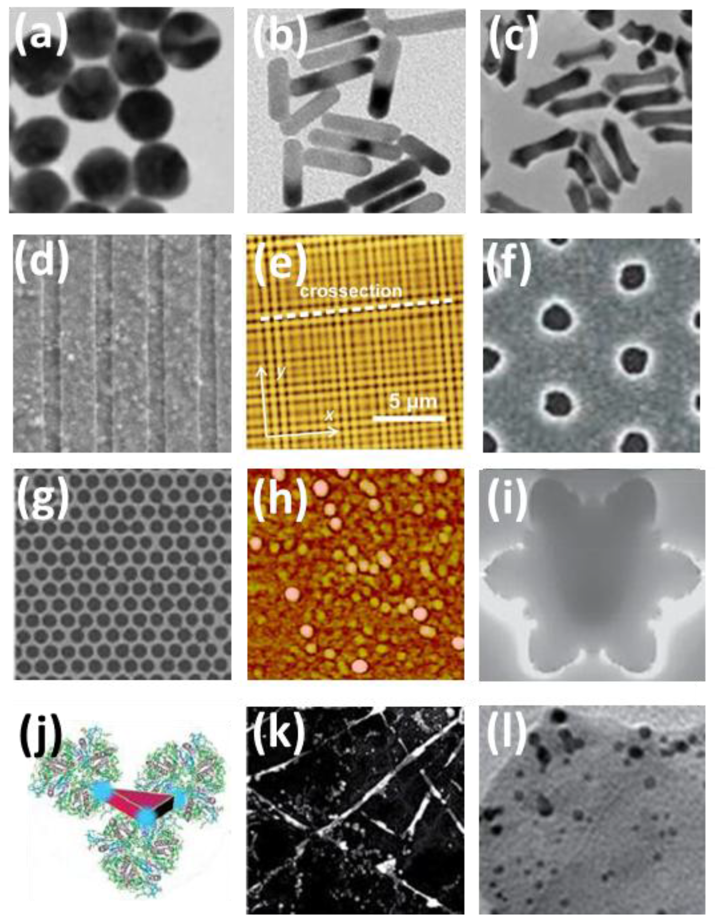
3. Material Nanostructures for Plasmonic Enhancement
4. Device Architectures for Plasmonic Enhancement
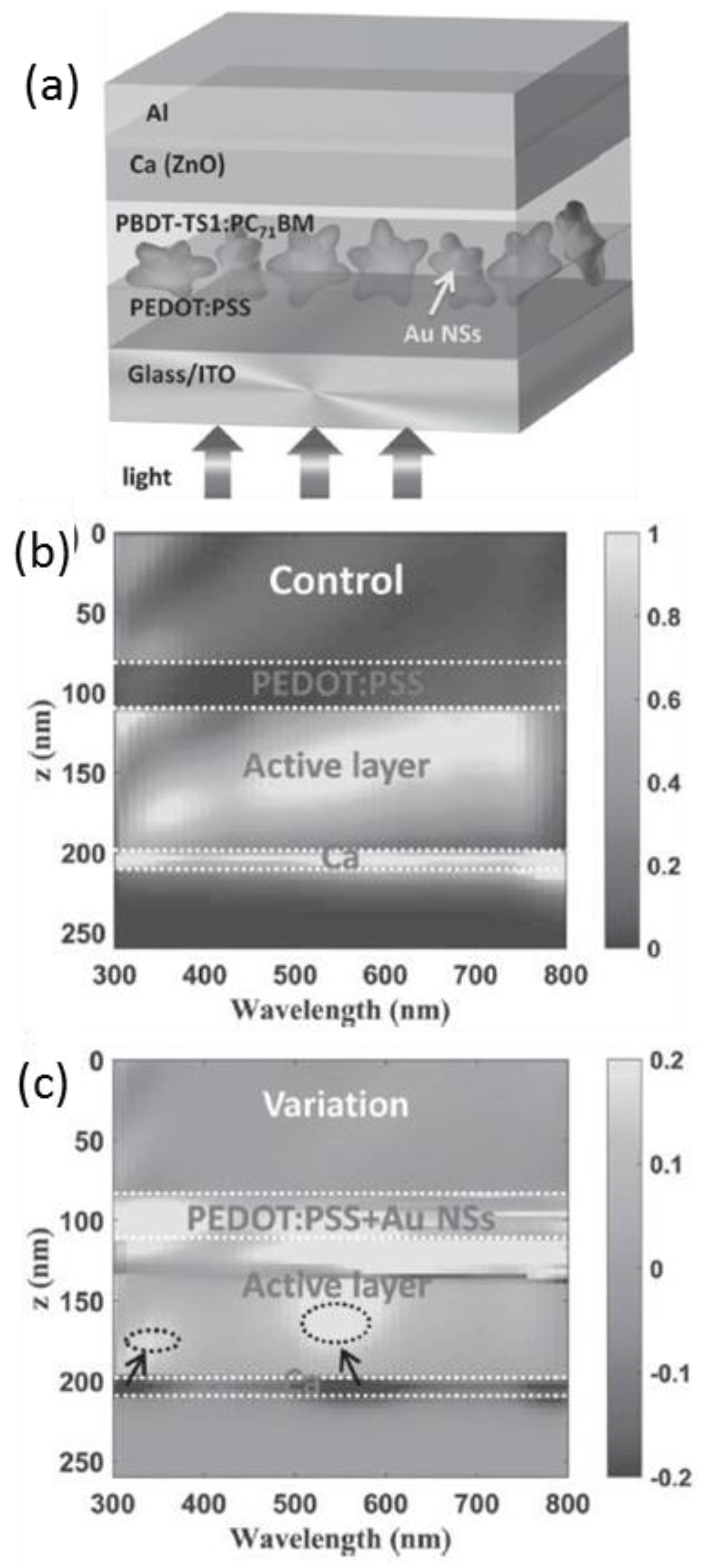
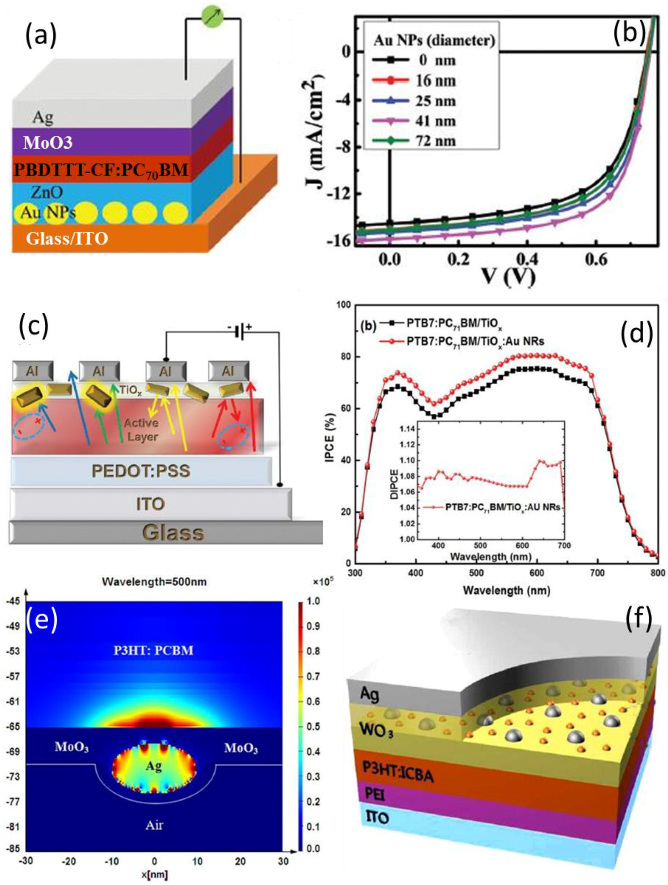
4.1. In the Active Layer
4.2. In Charge Transport Layer
4.3. Between the Active Layer and CTL
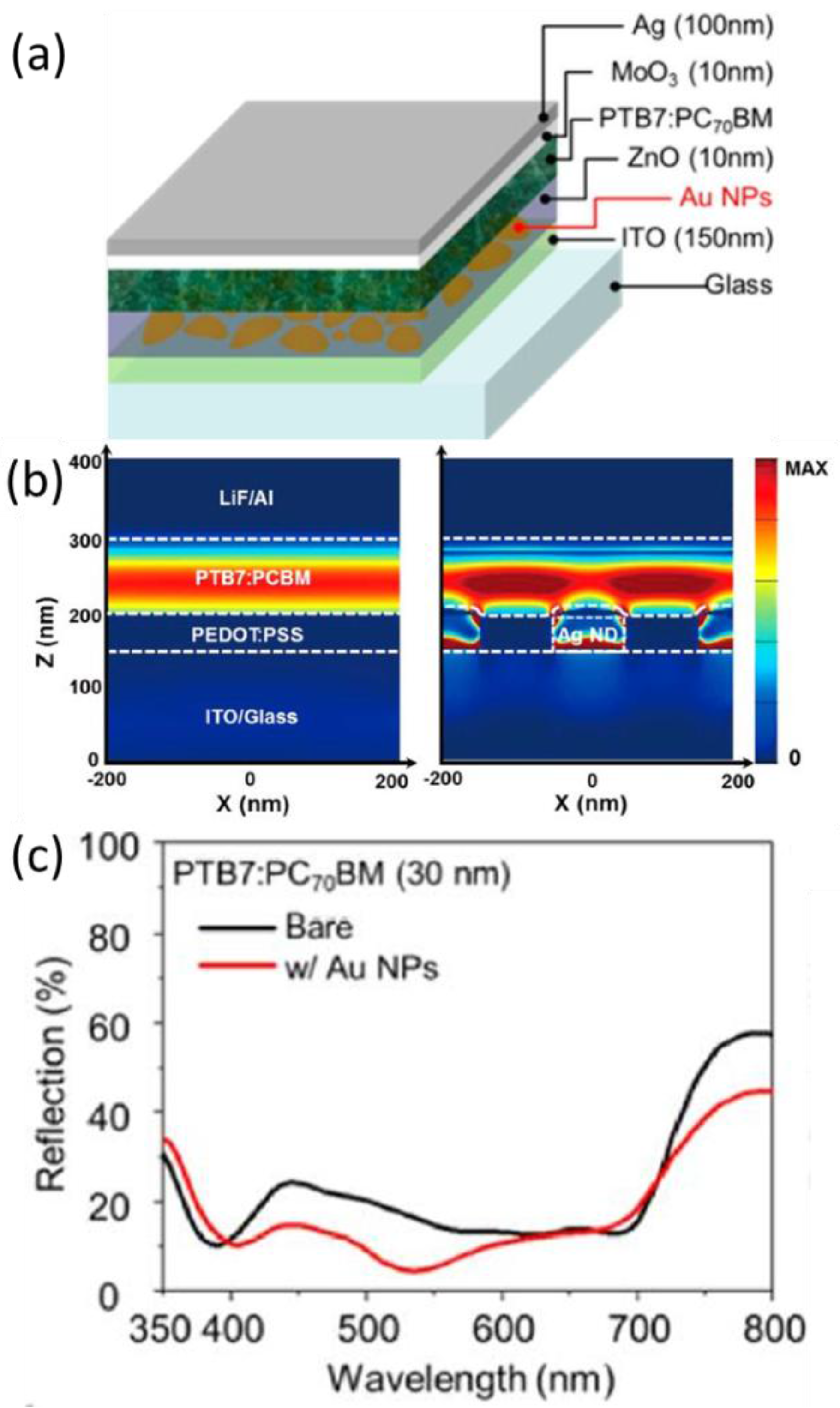
4.4. As Electrode
5. Photophysical Investigations of the Plasmonic Effect
5.1. Steady-State Characterizations of Absorption and Photoluminescence
5.1.1. To Confirm Plasmatic Effects Rendered by the Incorporation of Nanometals
5.1.2. To Elucidate Detailed Plasmonic Mechanisms
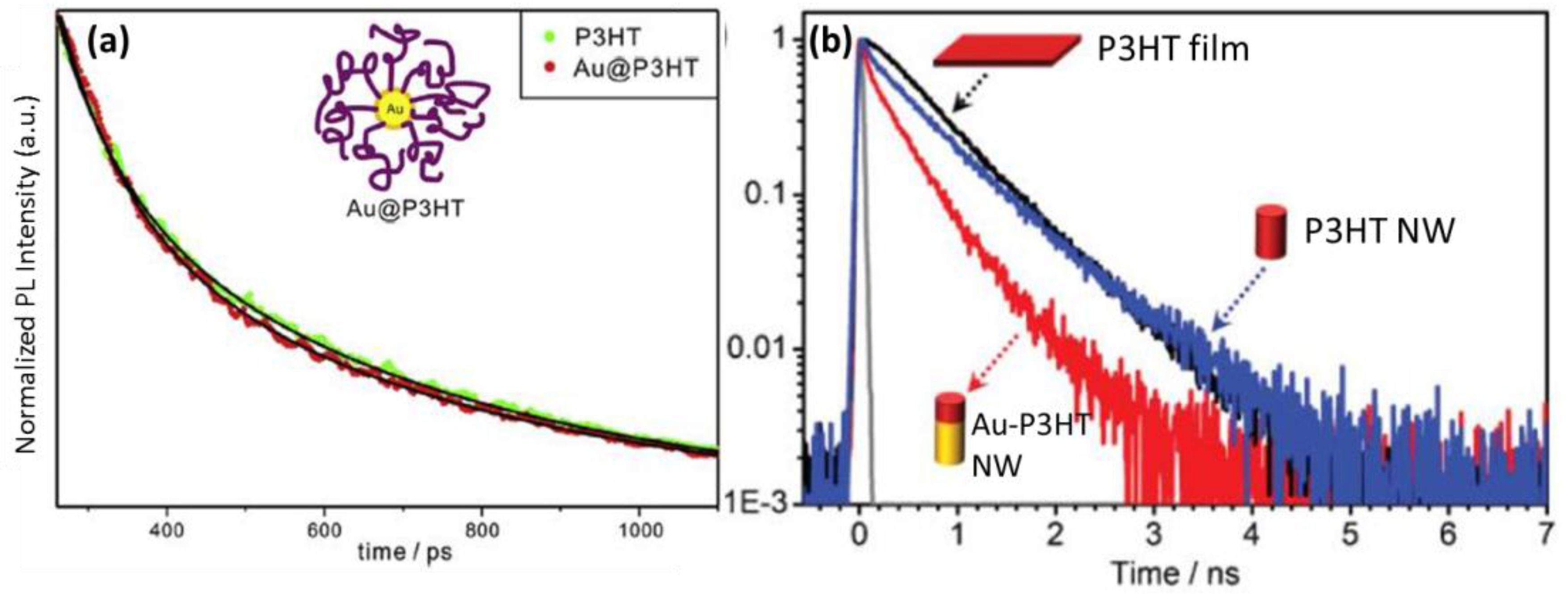
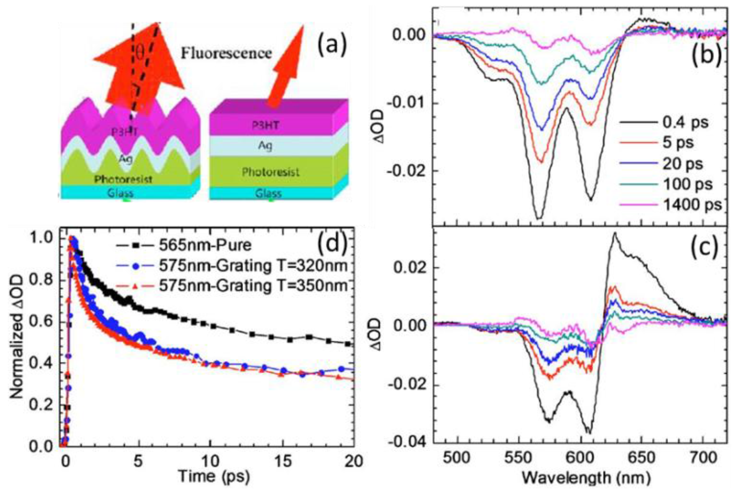
5.2. Transient Absorption and Photoluminescence Spectroscopies
6. Conclusions and Outlook
Acknowledgments
Conflicts of Interest
References
- Saga, T. Advances in crystalline silicon solar cell technology for industrial mass production. NPG Asia Mater. 2010, 2, 96–102. [Google Scholar] [CrossRef]
- Baran, D.; Ashraf, R.S.; Hanifi, D.A.; Abdelsamie, M.; Gasparini, N.; Rohr, J.A.; Holliday, S.; Wadsworth, A.; Lockett, S.; Neophytou, M.; et al. Reducing the efficiency-stability-cost gap of organic photovoltaics with highly efficient and stable small molecule acceptor ternary solar cells. Nat. Mater. 2017, 16, 363–369. [Google Scholar] [CrossRef] [PubMed]
- Li, M.; Gao, K.; Wan, X.; Zhang, Q.; Kan, B.; Xia, R.; Liu, F.; Yang, X.; Feng, H.; Ni, W.; et al. Solution-processed organic tandem solar cells with power conversion efficiencies >12%. Nat. Photonics 2016, 11, 85–90. [Google Scholar] [CrossRef]
- Zhao, W.C.; Li, S.S.; Yao, H.F.; Zhang, S.Q.; Zhang, Y.; Yang, B.; Hou, J.H. Molecular Optimization Enables over 13% Efficiency in Organic Solar Cells. J. Am. Chem. Soc. 2017, 139, 7148–7151. [Google Scholar] [CrossRef] [PubMed]
- Mayer, A.C.; Scully, S.R.; Hardin, B.E.; Rowell, M.W.; McGehee, M.D. Polymer-based solar cells. Mater. Today 2007, 10, 28–33. [Google Scholar] [CrossRef]
- Falke, S.M.; Rozzi, C.A.; Brida, D.; Maiuri, M.; Amato, M.; Sommer, E.; de Sio, A.; Rubio, A.; Cerullo, G.; Molinari, E.; et al. Coherent ultrafast charge transfer in an organic photovoltaic blend. Science 2014, 344, 1001–1005. [Google Scholar] [CrossRef] [PubMed]
- Wang, D.H.; Kim, D.Y.; Choi, K.W.; Seo, J.H.; Im, S.H.; Park, J.H.; Park, O.O.; Heeger, A.J. Enhancement of Donor-Acceptor Polymer Bulk Heterojunction Solar Cell Power Conversion Efficiencies by Addition of Au Nanoparticles. Angew. Chem. Int. Ed. 2011, 50, 5519–5523. [Google Scholar] [CrossRef] [PubMed]
- Park, H.I.; Lee, S.; Lee, J.M.; Nam, S.A.; Jeon, T.; Han, S.W.; Kim, S.O. High Performance Organic Photovoltaics with Plasmonic-Coupled Metal Nanoparticle Clusters. ACS Nano 2014, 8, 10305–10312. [Google Scholar] [CrossRef] [PubMed]
- Kozanoglu, D.; Apaydin, D.H.; Cirpan, A.; Esenturk, E.N. Power conversion efficiency enhancement of organic solar cells by addition of gold nanostars, nanorods, and nanospheres. Org. Electron. 2013, 14, 1720–1727. [Google Scholar] [CrossRef]
- Jung, K.; Song, H.J.; Lee, G.; Ko, Y.; Ahn, K.; Choi, H.; Kim, J.Y.; Ha, K.; Song, J.; Lee, J.K.; et al. Plasmonic Organic Solar Cells Employing Nanobump Assembly via Aerosol-Derived Nanoparticles. ACS Nano 2014, 8, 2590–2601. [Google Scholar] [CrossRef] [PubMed]
- Liu, C.M.; Chen, C.M.; Su, Y.W.; Wang, S.M.; Wei, K.H. The dual localized surface plasmonic effects of gold nanodots and gold nanoparticles enhance the performance of bulk heterojunction polymer solar cells. Org. Electron. 2013, 14, 2476–2483. [Google Scholar] [CrossRef]
- Xu, W.L.; Zeng, P.; Wu, B.; Zheng, F.; Zhu, F.R.; Smith, T.A.; Ghiggino, K.P.; Hao, X.T. Effects of Processing Solvent on the Photophysics and Nanomorphology of Poly(3-butyl-thiophene) Nanowires:PCBM Blends. J. Phys. Chem. Lett. 2016, 7, 1872–1879. [Google Scholar] [CrossRef] [PubMed]
- Gelinas, S.; Rao, A.; Kumar, A.; Smith, S.L.; Chin, A.W.; Clark, J.; van der Poll, T.S.; Bazan, G.C.; Friend, R.H. Ultrafast Long-Range Charge Separation in Organic Semiconductor Photovoltaic Diodes. Science 2014, 343, 512–516. [Google Scholar] [CrossRef] [PubMed]
- Banerji, N.; Cowan, S.; Vauthey, E.; Heeger, A.J. Ultrafast Relaxation of the Poly(3-hexylthiophene) Emission Spectrum. J. Phys. Chem. C 2011, 115, 9726–9739. [Google Scholar] [CrossRef]
- Liu, S.H.; Jiang, R.B.; You, P.; Zhu, X.Z.; Wang, J.F.; Yan, F. Au/Ag core-shell nanocuboids for high-efficiency organic solar cells with broadband plasmonic enhancement. Energy Environ. Sci. 2016, 9, 898–905. [Google Scholar] [CrossRef]
- Hergert, W.; Wriedt, T. The Mie Theory: Basics and Applications; Spinger: Berlin/Heidelberg, Germany, 2012; Volume 169. [Google Scholar]
- Atwater, H.A.; Polman, A. Plasmonics for improved photovoltaic devices (vol 9, pg 205, 2010). Nat. Mater. 2010, 9, 865. [Google Scholar] [CrossRef]
- Ferry, V.E.; Sweatlock, L.A.; Pacifici, D.; Atwater, H.A. Plasmonic Nanostructure Design for Efficient Light Coupling into Solar Cells. Nano Lett. 2008, 8, 4391–4397. [Google Scholar] [CrossRef] [PubMed]
- Li, X.H.; Choy, W.C.H.; Lu, H.F.; Sha, W.E.I.; Ho, A.H.P. Efficiency Enhancement of Organic Solar Cells by Using Shape-Dependent Broadband Plasmonic Absorption in Metallic Nanoparticles. Adv. Funct. Mater. 2013, 23, 2728–2735. [Google Scholar] [CrossRef]
- Morawiec, S.; Mendes, M.J.; Filonovich, S.A.; Mateus, T.; Mirabella, S.; Aguas, H.; Ferreira, I.; Simone, F.; Fortunato, E.; Martins, R.; et al. Broadband photocurrent enhancement in a-Si:H solar cells with plasmonic back reflectors. Opt. Express 2014, 22, A1059–A1070. [Google Scholar] [CrossRef] [PubMed]
- Yao, K.; Salvador, M.; Chueh, C.C.; Xin, X.K.; Xu, Y.X.; de Quilettes, D.W.; Hu, T.; Chen, Y.W.; Ginger, D.S.; Jen, A.K.Y. A General Route to Enhance Polymer Solar Cell Performance using Plasmonic Nanoprisms. Adv. Energy Mater. 2014, 4, 1289–1295. [Google Scholar] [CrossRef]
- Baek, S.W.; Noh, J.; Lee, C.H.; Kim, B.; Seo, M.K.; Lee, J.Y. Plasmonic Forward Scattering Effect in Organic Solar Cells: A Powerful Optical Engineering Method. Sci. Rep. 2013, 3, 1726. [Google Scholar] [CrossRef]
- Salvador, M.; MacLeod, B.A.; Hess, A.; Kulkarni, A.P.; Munechika, K.; Chen, J.I.L.; Ginger, D.S. Electron Accumulation on Metal Nanoparticles in Plasmon-Enhanced Organic Solar Cells. ACS Nano 2012, 6, 10024–10032. [Google Scholar] [CrossRef] [PubMed]
- Mokkapati, S.; Beck, F.J.; de Waele, R.; Polman, A.; Catchpole, K.R. Resonant nano-antennas for light trapping in plasmonic solar cells. J. Phys. D 2011, 44, 185101. [Google Scholar] [CrossRef]
- Gan, Q.Q.; Bartoli, F.J.; Kafafi, Z.H. Plasmonic-Enhanced Organic Photovoltaics: Breaking the 10% Efficiency Barrier. Adv. Mater. 2013, 25, 2385–2396. [Google Scholar] [CrossRef] [PubMed]
- Wu, B.; Wu, X.; Guan, C.; Tai, K.F.; Yeow, E.K.; Fan, H.J.; Mathews, N.; Sum, T.C. Uncovering loss mechanisms in silver nanoparticle-blended plasmonic organic solar cells. Nat. Commun. 2013, 4, 2004. [Google Scholar] [CrossRef] [PubMed]
- Spyropoulos, G.D.; Stylianakis, M.M.; Stratakis, E.; Kymakis, E. Organic bulk heterojunction photovoltaic devices with surfactant-free Au nanoparticles embedded in the active layer. Appl. Phys. Lett. 2012, 100, 213904. [Google Scholar] [CrossRef]
- Jang, Y.H.; Jang, Y.J.; Kim, S.; Quan, L.N.; Chung, K.; Kim, D.H. Plasmonic Solar Cells: From Rational Design to Mechanism Overview. Chem. Rev. 2016, 116, 14982–15034. [Google Scholar] [CrossRef] [PubMed]
- Sharma, B.; Frontiera, R.R.; Henry, A.I.; Ringe, E.; van Duyne, R.P. SERS: Materials, applications, and the future. Mater. Today 2012, 15, 16–25. [Google Scholar] [CrossRef]
- Lim, E.L.; Yap, C.C.; Teridi, M.A.M.; Teh, C.H.; Yusoff, A.R.B.M.; Jumali, M.H.H. A review of recent plasmonic nanoparticles incorporated P3HT: PCBM organic thin film solar cells. Org. Electron. 2016, 36, 12–28. [Google Scholar] [CrossRef]
- Morfa, A.J.; Rowlen, K.L.; Reilly, T.H.; Romero, M.J.; van de Lagemaat, J. Plasmon-enhanced solar energy conversion in organic bulk heterojunction photovoltaics. Appl. Phys. Lett. 2008, 92, 013504. [Google Scholar] [CrossRef]
- Stratakis, E.; Kymakis, E. Nanoparticle-based plasmonic organic photovoltaic devices. Mater. Today 2013, 16, 133–146. [Google Scholar] [CrossRef]
- Paci, B.; Spyropoulos, G.D.; Generosi, A.; Bailo, D.; Albertini, V.R.; Stratakis, E.; Kymakis, E. Enhanced Structural Stability and Performance Durability of Bulk Heterojunction Photovoltaic Devices Incorporating Metallic Nanoparticles. Adv. Funct. Mater. 2011, 21, 3573–3582. [Google Scholar] [CrossRef]
- Raether, H. Surface Plasmons; Springer: Berlin, Germany, 1988. [Google Scholar]
- Li, X.H.; Sha, W.E.I.; Choy, W.C.H.; Fung, D.D.S.; Xie, F.X. Efficient Inverted Polymer Solar Cells with Directly Patterned Active Layer and Silver Back Grating. J. Phys. Chem. C 2012, 116, 7200–7206. [Google Scholar] [CrossRef]
- Zhou, L.; Jiang, X.C.; Li, Y.Q.; Shi, A.L.; Chen, J.D.; Ou, Q.D.; Liu, H.T.; Tang, J.X. Light Extraction of Trapped Optical Modes in Polymer Light-Emitting Diodes with Nanoimprinted Double-Pattern Gratings. ACS Appl. Mater. Interfaces 2014, 6, 18139–18146. [Google Scholar] [CrossRef] [PubMed]
- Choi, M.; Kang, G.; Shin, D.; Barange, N.; Lee, C.W.; Ko, D.H.; Kim, K. Lithography-Free Broadband Ultrathin-Film Absorbers with Gap-Plasmon Resonance for Organic Photovoltaics. ACS Appl. Mater. Interfaces 2016, 8, 12997–13008. [Google Scholar] [CrossRef] [PubMed]
- Ahn, S.; Rourke, D.; Park, W. Plasmonic nanostructures for organic photovoltaic devices. J. Opt. 2016, 18, 033001. [Google Scholar] [CrossRef]
- Lassiter, J.B.; McGuire, F.; Mock, J.J.; Ciraci, C.; Hill, R.T.; Wiley, B.J.; Chilkoti, A.; Smith, D.R. Plasmonic Waveguide Modes of Film-Coupled Metallic Nanocubes. Nano Lett. 2013, 13, 5866–5872. [Google Scholar] [CrossRef] [PubMed]
- Chou, C.H.; Chen, F.C. Plasmonic nanostructures for light trapping in organic photovoltaic devices. Nanoscale 2014, 6, 8444–8458. [Google Scholar] [CrossRef] [PubMed]
- Moreau, A.; Ciraci, C.; Mock, J.J.; Hill, R.T.; Wang, Q.; Wiley, B.J.; Chilkoti, A.; Smith, D.R. Controlled-reflectance surfaces with film-coupled colloidal nanoantennas. Nature 2012, 492, 86–89. [Google Scholar] [CrossRef] [PubMed]
- Kreibig, U.; Vollmer, M. Optical Properties of Metal Clusters; Springer: Berlin, Germany, 1995; Volume 25. [Google Scholar]
- Wang, D.-D.; Ge, C.-W.; Wu, G.-A.; Li, Z.-P.; Wang, J.-Z.; Zhang, T.-F.; Yu, Y.-Q.; Luo, L.-B. A sensitive red light nano-photodetector propelled by plasmonic copper nanoparticles. J. Mater. Chem. C 2017, 5, 1328–1335. [Google Scholar] [CrossRef]
- Bharti, A.; Bhardwaj, R.; Agrawal, A.K.; Goyal, N.; Gautam, S. Monochromatic X-Ray Induced Novel Synthesis of Plasmonic Nanostructure for Photovoltaic Application. Sci. Rep. 2016, 6, 22394. [Google Scholar] [CrossRef] [PubMed]
- Ferry, V.E.; Munday, J.N.; Atwater, H.A. Design considerations for plasmonic photovoltaics. Adv. Mater. 2010, 22, 4794–4808. [Google Scholar] [CrossRef] [PubMed]
- Gao, Y.; Jin, F.; Su, Z.; Zhao, H.; Luo, Y.; Chu, B.; Li, W. Cooperative plasmon enhanced organic solar cells with thermal coevaporated Au and Ag nanoparticles. Org. Electron. 2017, 48, 336–341. [Google Scholar] [CrossRef]
- Li, X.H.; Ren, X.G.; Xie, F.X.; Zhang, Y.X.; Xu, T.T.; Wei, B.Q.; Choy, W.C.H. High-Performance Organic Solar Cells with Broadband Absorption Enhancement and Reliable Reproducibility Enabled by Collective Plasmonic Effects. Adv. Opt. Mater. 2015, 3, 1220–1231. [Google Scholar] [CrossRef]
- Lu, L.Y.; Luo, Z.Q.; Xu, T.; Yu, L.P. Cooperative Plasmonic Effect of Ag and Au Nanoparticles on Enhancing Performance of Polymer Solar Cells. Nano Lett. 2013, 13, 59–64. [Google Scholar] [CrossRef] [PubMed]
- Ji, T.; Peng, L.N.; Zhu, Y.T.; Yang, F.; Cui, Y.X.; Wu, X.Y.; Liu, L.; He, S.L.; Zhu, F.R.; Hao, Y.Y. Plasmonic broadband absorber by stacking multiple metallic nanoparticle layers. Appl. Phys. Lett. 2015, 106, 161107. [Google Scholar] [CrossRef]
- Chirumamilla, M.; Gopalakrishnan, A.; Toma, A.; Zaccaria, R.P.; Krahne, R. Plasmon resonance tuning in metal nanostars for surface enhanced Raman scattering. Nanotechnology 2014, 25, 235303. [Google Scholar] [CrossRef] [PubMed]
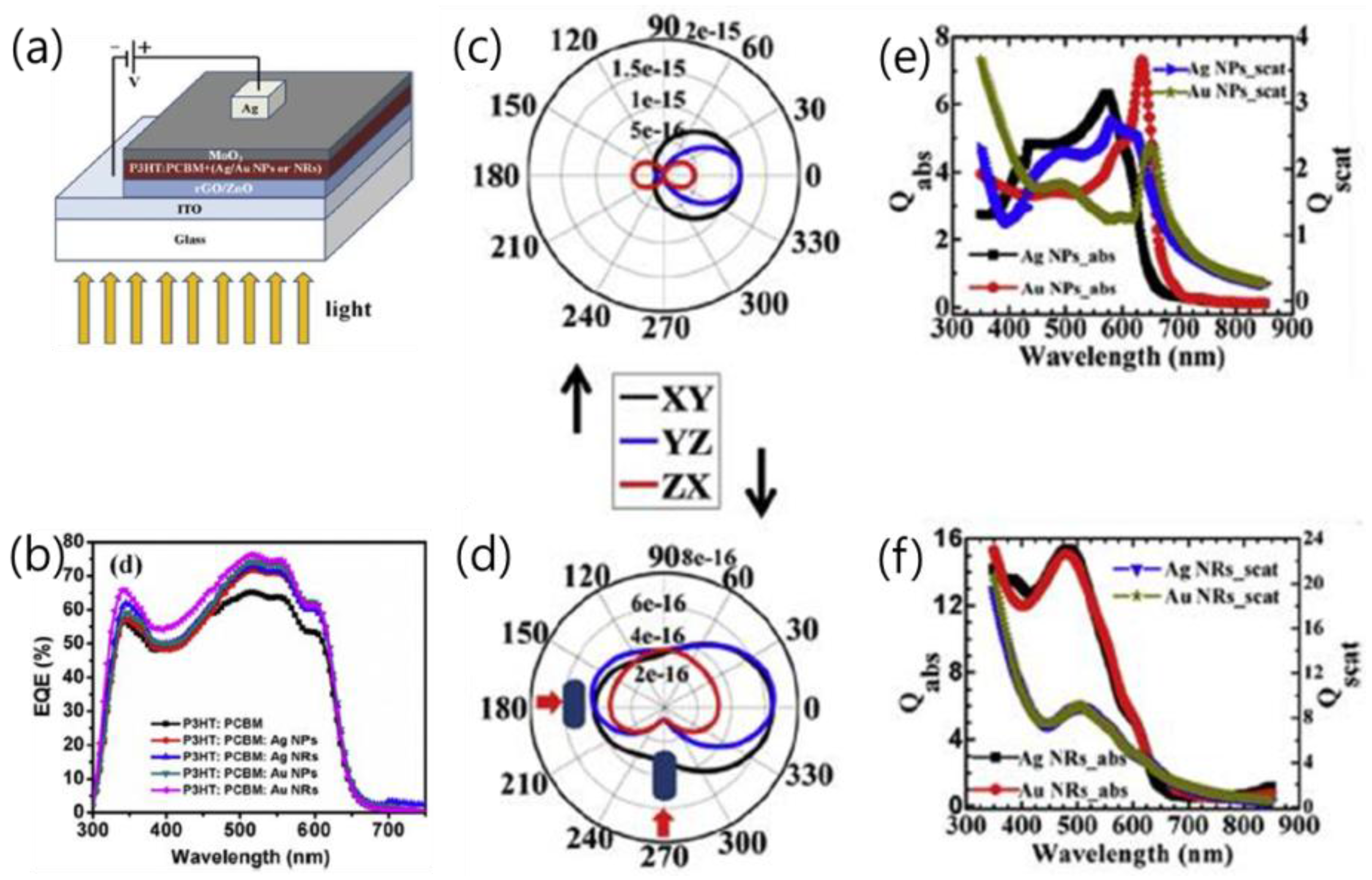
- Gollu, S.R.; Sharma, R.; Srinivas, G.; Kundu, S.; Gupta, D. Incorporation of silver and gold nanostructures for performance improvement in P3HT: PCBM inverted solar cell with rGO/ZnO nanocomposite as an electron transport layer. Org. Electron. 2016, 29, 79–87. [Google Scholar] [CrossRef]
- Sygletou, M.; Tzourmpakis, P.; Petridis, C.; Konios, D.; Fotakis, C.; Kymakis, E.; Stratakis, E. Laser induced nucleation of plasmonic nanoparticles on two-dimensional nanosheets for organic photovoltaics. J. Mater. Chem. A 2016, 4, 1020–1027. [Google Scholar] [CrossRef]
- Ren, X.; Cheng, J.; Zhang, S.; Li, X.; Rao, T.; Huo, L.; Hou, J.; Choy, W.C. High Efficiency Organic Solar Cells Achieved by the Simultaneous Plasmon-Optical and Plasmon-Electrical Effects from Plasmonic Asymmetric Modes of Gold Nanostars. Small 2016, 12, 5200–5207. [Google Scholar] [CrossRef] [PubMed]
- Yao, M.; Shen, P.; Liu, Y.; Chen, B.; Guo, W.; Ruan, S.; Shen, L. Performance Improvement of Polymer Solar Cells by Surface-Energy-Induced Dual Plasmon Resonance. ACS Appl. Mater. Interfaces 2016, 8, 6183–6189. [Google Scholar] [CrossRef] [PubMed]
- Yao, K.; Jiao, H.; Xu, Y.-X.; He, Q.; Li, F.; Wang, X. Nano-bio hybrids of plasmonic metals/photosynthetic proteins for broad-band light absorption enhancement in organic solar cells. J. Mater. Chem. A 2016, 4, 13400–13406. [Google Scholar] [CrossRef]
- Nardes, A.M.; Ahn, S.; Rourke, D.; Mao, C.; van de Lagemaat, J.; Ferguson, A.J.; Park, W.; Kopidakis, N. Integrating nanostructured electrodes in organic photovoltaic devices for enhancing near-infrared photoresponse. Org. Electron. 2016, 39, 59–63. [Google Scholar] [CrossRef]
- Khan, I.; Keshmiri, H.; Kolb, F.; Dimopoulos, T.; List-Kratochvil, E.J.W.; Dostalek, J. Multidiffractive Broadband Plasmonic Absorber. Adv. Opt. Mater. 2016, 4, 435–443. [Google Scholar] [CrossRef]
- Liapis, A.C.; Sfeir, M.Y.; Black, C.T. Plasmonic hole arrays for combined photon and electron management. Appl. Phys. Lett. 2016, 109, 201101. [Google Scholar] [CrossRef]
- Stelling, C.; Singh, C.R.; Karg, M.; Konig, T.A.; Thelakkat, M.; Retsch, M. Plasmonic nanomeshes: Their ambivalent role as transparent electrodes in organic solar cells. Sci. Rep. 2017, 7, 42530. [Google Scholar] [CrossRef] [PubMed]
- Kou, P.; Yang, L.; Chang, C.; He, S. Improved Flexible Transparent Conductive Electrodes based on Silver Nanowire Networks by a Simple Sunlight Illumination Approach. Sci. Rep. 2017, 7, 42052. [Google Scholar] [CrossRef] [PubMed]
- Hornich, J.; Pflaum, C.; Brabec, C.; Forberich, K. Numerical study of plasmonic absorption enhancement in semiconductor absorbers by metallic nanoparticles. J. Appl. Phys. 2016, 120, 113102. [Google Scholar] [CrossRef]
- Malureanu, R.; Lavrinenko, A. Ultra-thin films for plasmonics: A technology overview. Nanotechnol. Rev. 2015, 4, 259–275. [Google Scholar] [CrossRef]
- Lee, J.; Lee, A.; Yu, H.K. Graphene protected Ag nanowires: Blocking of surface migration for thermally stable and wide-range-wavelength transparent flexible electrodes. RSC Adv. 2016, 6, 84985–84989. [Google Scholar] [CrossRef]
- Stylianakis, M.M.; Konios, D.; Petridis, C.; Kakavelakis, G.; Stratakis, E.; Kymakis, E. Ternary solution-processed organic solar cells incorporating 2D materials. 2D Mater. 2017, 4, 042005. [Google Scholar] [CrossRef]
- Lange, P.; Kewes, G.; Severin, N.; Benson, O.; Rabe, J.P. Evidence for Graphene Plasmons in the Visible Spectral Range Probed by Molecules. arXiv, 2014; arXiv:1404. [Google Scholar]
- Choy, W.C.H.; Xingang, R. Plasmon-Electrical Effects on Organic Solar Cells by Incorporation of Metal Nanostructures. IEEE J. Sel. Top. Quantum Electron. 2016, 22, 1–9. [Google Scholar] [CrossRef]
- You, J.; Takahashi, Y.; Leonard, K.; Yonemura, H.; Yamada, S. Influence of space arrangement of silver nanoparticles in organic photoelectric conversion devices. J. Photochem. Photobiol. A Chem. 2017, 332, 586–594. [Google Scholar] [CrossRef]
- Paci, B.; Kakavelakis, G.; Generosi, A.; Wright, J.; Ferrero, C.; Stratakis, E.; Kymakis, E. Improving stability of organic devices: A time/space resolved structural monitoring approach applied to plasmonic photovoltaics. Sol. Energy Mater. Sol. Cells 2017, 159, 617–624. [Google Scholar] [CrossRef]
- Zhang, R.; Zhou, Y.; Peng, L.; Li, X.; Chen, S.; Feng, X.; Guan, Y.; Huang, W. Influence of SiO2 shell thickness on power conversion efficiency in plasmonic polymer solar cells with Au nanorod@SiO2 core-shell structures. Sci. Rep. 2016, 6, 25036. [Google Scholar] [CrossRef] [PubMed]
- Kakavelakis, G.; Vangelidis, I.; Heuer-Jungemann, A.; Kanaras, A.G.; Lidorikis, E.; Stratakis, E.; Kymakis, E. Plasmonic Backscattering Effect in High-Efficient Organic Photovoltaic Devices. Adv. Energy Mater. 2016, 6, 1501640. [Google Scholar] [CrossRef]
- Hu, T.; Li, L.; Xiao, S.; Yuan, K.; Yang, H.; Chen, L.; Chen, Y. In situ implanting carbon nanotube-gold nanoparticles into ZnO as efficient nanohybrid cathode buffer layer for polymer solar cells. Org. Electron. 2016, 38, 350–356. [Google Scholar] [CrossRef]
- Li, S.; Li, Z.; Zhang, X.; Zhang, Z.; Liu, C.; Shen, L.; Guo, W.; Ruan, S. Performance enhancement of organic photovoltaic devices enabled by Au nanoarrows inducing surface plasmonic resonance effect. Phys. Chem. Chem. Phys. 2016, 18, 24285–24289. [Google Scholar] [CrossRef] [PubMed]
- Chi, D.; Lu, S.; Xu, R.; Liu, K.; Cao, D.; Wen, L.; Mi, Y.; Wang, Z.; Lei, Y.; Qu, S.; Wang, Z. Fully understanding the positive roles of plasmonic nanoparticles in ameliorating the efficiency of organic solar cells. Nanoscale 2015, 7, 15251–15257. [Google Scholar] [CrossRef] [PubMed]
- Shen, P.; Liu, Y.; Long, Y.; Shen, L.; Kang, B. High-Performance Polymer Solar Cells Enabled by Copper Nanoparticles-Induced Plasmon Resonance Enhancement. J. Phys. Chem. C 2016, 120, 8900–8906. [Google Scholar] [CrossRef]
- Dang, P.T.; Nguyen, T.K.; Le, K.Q. Revisited design optimization of metallic gratings for plasmonic light-trapping enhancement in thin organic solar cells. Opt. Commun. 2017, 382, 241–245. [Google Scholar] [CrossRef]
- Oh, Y.; Lim, J.W.; Kim, J.G.; Wang, H.; Kang, B.H.; Park, Y.W.; Kim, H.; Jang, Y.J.; Kim, J.; Kim, D.H.; et al. Plasmonic Periodic Nanodot Arrays via Laser Interference Lithography for Organic Photovoltaic Cells with >10% Efficiency. ACS Nano 2016, 10, 10143–10151. [Google Scholar] [CrossRef] [PubMed]
- In, S.; Park, N. Inverted Ultrathin Organic Solar Cells with a Quasi-Grating Structure for Efficient Carrier Collection and Dip-less Visible Optical Absorption. Sci. Rep. 2016, 6, 21784. [Google Scholar] [CrossRef] [PubMed]
- Nagamani, S.; Kumarasamy, G.; Song, M.; Kim, C.S.; Kim, D.-H.; Ryu, S.Y.; Kang, J.-W.; Jin, S.-H. Optical absorption and electrical properties of enhanced efficiency in organic solar cells as interfacial layer with Au NPs. Synth. Met. 2016, 217, 117–122. [Google Scholar] [CrossRef]
- Yang, Y.; Qing, J.; Ou, J.; Lin, X.; Yuan, Z.; Yu, D.; Zhou, X.; Chen, X. Rational design of metallic nanowire-based plasmonic architectures for efficient inverted polymer solar cells. Sol. Energy 2015, 122, 231–238. [Google Scholar] [CrossRef]
- Chalh, M.; Vedraine, S.; Lucas, B.; Ratier, B. Plasmonic Ag nanowire network embedded in zinc oxide nanoparticles for inverted organic solar cells electrode. Sol. Energy Mater. Sol. Cells 2016, 152, 34–41. [Google Scholar] [CrossRef]
- Hara, K.; Lertvachirapaiboon, C.; Ishikawa, R.; Ohdaira, Y.; Shinbo, K.; Kato, K.; Kaneko, F.; Baba, A. Inverted organic solar cells enhanced by grating-coupled surface plasmons and waveguide modes. Phys. Chem. Chem. Phys. 2017, 19, 2791–2796. [Google Scholar] [CrossRef] [PubMed]
- Pathak, H.; Pathak, N.K.; Ji, A.; Roopak, S.; Pandey, G.K.; Sharma, R.P. Broadband Scattering With Strong Electric Field Coupling Between Metal Nanostructures Using DDA Simulation: Role of Different Organic Environments. IEEE J. Photovolt. 2016, 6, 940–951. [Google Scholar] [CrossRef]
- Hsiao, Y.-S.; Charan, S.; Wu, F.-Y.; Chien, F.-C.; Chu, C.-W.; Chen, P.; Chen, F.-C. Improving the Light Trapping Efficiency of Plasmonic Polymer Solar Cells through Photon Management. J. Phys. Chem. C 2012, 116, 20731–20737. [Google Scholar] [CrossRef]
- Sha, W.E.; Zhu, H.L.; Chen, L.; Chew, W.C.; Choy, W.C. A general design rule to manipulate photocarrier transport path in solar cells and its realization by the plasmonic-electrical effect. Sci. Rep. 2015, 5, 8525. [Google Scholar] [CrossRef] [PubMed]
- Rana, A.; Gupta, N.; Lochan, A.; Sharma, G.D.; Chand, S.; Kumar, M.; Singh, R.K. Charge carrier dynamics and surface plasmon interaction in gold nanorod-blended organic solar cell. J. Appl. Phys. 2016, 120, 063102. [Google Scholar] [CrossRef]
- Peng, B.; Liu, X.; Ji, Y.; Demir, H.V.; Huang, C.H.A.; Sum, T.C.; Xiong, Q. Fluorophore-doped core-multishell spherical plasmonic nanocavities: resonant energy transfer toward a loss compensation. ACS Nano 2012, 7, 6250–6259. [Google Scholar]
- Kakavelakis, G.; Castillo, A.E.D.; Pellegrini, V.; Ansaldo, A.; Tzourmpakis, P.; Brescia, R.; Prato, M.; Stratakis, E.; Kymakis, E.; Bonaccorso, F. Size-Tuning of WSe2 Flakes for High Efficiency Inverted Organic Solar Cells. ACS Nano 2017, 11, 3517–3531. [Google Scholar] [CrossRef] [PubMed]
- Zhang, G.; Hawks, S.A.; Ngo, C.; Schelhas, L.T.; Scholes, D.T.; Kang, H.; Aguirre, J.C.; Tolbert, S.H.; Schwartz, B.J. Extensive Penetration of Evaporated Electrode Metals into Fullerene Films: Intercalated Metal Nanostructures and Influence on Device Architecture. ACS Appl. Mater. Interfaces 2015, 7, 25247–25258. [Google Scholar] [CrossRef] [PubMed]
- Xu, P.; Shen, L.; Meng, F.; Zhang, J.; Xie, W.; Yu, W.; Guo, W.; Jia, X.; Ruan, S. The role of Ag nanoparticles in inverted polymer solar cells: Surface plasmon resonance and backscattering centers. Appl. Phys. Lett. 2013, 102, 123301. [Google Scholar] [CrossRef]
- Lee, C.; Wei, X.D.; Kysar, J.W.; Hone, J. Measurement of the elastic properties and intrinsic strength of monolayer graphene. Science 2008, 321, 385–388. [Google Scholar] [CrossRef] [PubMed]
- El-Kady, M.F.; Strong, V.; Dubin, S.; Kaner, R.B. Laser Scribing of High-Performance and Flexible Graphene-Based Electrochemical Capacitors. Science 2012, 335, 1326–1330. [Google Scholar] [CrossRef] [PubMed]
- Li, Y.F.; Dong, F.X.; Chen, Y.; Zhang, X.L.; Wang, L.; Bi, Y.G.; Tian, Z.N.; Liu, Y.F.; Feng, J.; Sun, H.B. As-grown graphene/copper nanoparticles hybrid nanostructures for enhanced intensity and stability of surface plasmon resonance. Sci. Rep. 2016, 6, 8. [Google Scholar] [CrossRef] [PubMed]
- Du, P.; Jing, P.; Li, D.; Cao, Y.; Liu, Z.; Sun, Z. Plasmonic Ag@oxide nanoprisms for enhanced performance of organic solar cells. Small 2015, 11, 2454–2462. [Google Scholar] [CrossRef] [PubMed]
- Smolarek, K.; Ebenhoch, B.; Czechowski, N.; Prymaczek, A.; Twardowska, M.; Samuel, I.D.W.; Mackowski, S. Silver nanowires enhance absorption of poly(3-hexylthiophene). Appl. Phys. Lett. 2013, 103, 203302. [Google Scholar] [CrossRef]
- O’Carroll, D.M.; Hofmann, C.E.; Atwater, H.A. Conjugated polymer/metal nanowire heterostructure plasmonic antennas. Adv. Mater. 2010, 22, 1223–1227. [Google Scholar] [CrossRef] [PubMed]
- Bohren, C.F.; Huffman, D.R. Absorption and Scattering of Light by Small Particles; Wiley-Interscience: New York, NY, USA, 1983. [Google Scholar]
- Zayats, A.V.; Smolyaninov, I.I.; Maradudin, A.A. Nano-optics of surface plasmon polaritons. Phys. Rep. 2005, 408, 131–314. [Google Scholar] [CrossRef]
- Bozhevolnyi, S.I.; Smolyaninov, I.I.; Zayats, A.V. Near-field microscopy of surface-plasmon polaritons: Localization and internal interface imaging. Phys. Rev. B 1995, 51, 17916–17924. [Google Scholar] [CrossRef]
- Atay, T.; Song, J.H.; Nurmikko, A.V. Strongly interacting plasmon nanoparticle pairs: From dipole-dipole interaction to conductively coupled regime. Nano Lett. 2004, 4, 1627–1631. [Google Scholar] [CrossRef]
- Liu, Z.; Liu, X.; Huang, S.; Pan, P.; Chen, J.; Liu, G.; Gu, G. Automatically acquired broadband plasmonic-metamaterial black absorber during the metallic film-formation. ACS Appl. Mater. Interfaces 2015, 7, 4962–4968. [Google Scholar] [CrossRef] [PubMed]
- Paci, B.; Generosi, A.; Albertini, V.R.; Spyropoulos, G.D.; Stratakis, E.; Kymakis, E. Enhancement of photo/thermal stability of organic bulk heterojunction photovoltaic devices via gold nanoparticles doping of the active layer. Nanoscale 2012, 4, 7452–7459. [Google Scholar] [CrossRef] [PubMed]
- Korovyanko, O.J.; Osterbacka, R.; Jiang, X.M.; Vardeny, Z.V.; Janssen, R.A.J. Photoexcitation dynamics in regioregular and regiorandom polythiophene films. Phys. Rev. B 2001, 64, 235122-1/6. [Google Scholar] [CrossRef]
- Lee, D.; Jang, D.-J. Charge-carrier relaxation dynamics of poly(3-hexylthiophene)-coated gold hybrid nanoparticles. Polymer 2014, 55, 5469–5476. [Google Scholar] [CrossRef]
- Bhattacharyya, S.; Patra, A. Photoluminescence quenching of semiconducting polymer nanoparticles in presence of Au nanoparticles. Bull. Mater. Sci. 2012, 35, 719–725. [Google Scholar] [CrossRef]
- Wang, H.; Wang, H.-Y.; Gao, B.-R.; Jiang, Y.; Yang, Z.-Y.; Hao, Y.-W.; Chen, Q.-D.; Du, X.-B.; Sun, H.-B. Surface plasmon enhanced absorption dynamics of regioregular poly(3-hexylthiophene). Appl. Phys. Lett. 2011, 98, 251501. [Google Scholar] [CrossRef]


| System | Configuration | Mechanism | Short-Circuit Current Jsc | Open-Circuit Voltage (Voc) | Fill Factor (FF) | PCE | Enhancement |
|---|---|---|---|---|---|---|---|
| P3HT: PCBM: Ag NPs [68] | control In active layer | LSPR | 8.67 10.41 | 0.60 0.60 | 61.4 62.8 | 3.19 3.92 | ~23% in PCE |
| P3HT:PCBM:Ag NPs/NRs in active layer [51] | control Ag NPs Ag NRs Au NPs Au NRs | LSPR | 9.49 10.60 10.99 11.17 12.21 | 0.63 0.63 0.63 0.63 0.63 | 63.47 63.61 63.64 63.70 63.75 | 3.77 4.21 4.37 4.44 4.85 | ~28% in PCE |
| PCDTBT:PC71BM: WS2-Au [52] | control In active layer | LSPR | 10.6 12.3 | 0.89 0.89 | 60.2 58.4 | 5.6 6.3 | ~13% in PCE |
| PBDT-TS1:PC71BM Au nanostars in active and PEDOT [53] | control In active and HTL | asymmetric modes | 18.37 19.24 | 0.81 0.81 | 67.00 67.70 | 9.97 10.50 | ~5% in PCE |
| PEDOT/Au NR@ SiO2/PTB7:PC71BM [69] | control between CTL and active layer | Scattering, LSPR | 16.5 21.2 | 0.74 0.74 | 0.60 0.60 | 7.52 9.55 | ~28% in PCE |
| PCDTBT:PC71BM/Au NRs in TiOx PTB7:PC71BM/Au NRs in TiOx [70] | control Au NRs in back ETL control Au NRs in back ETL | Backward scattering Backward scattering | 10.87 12.03 16.27 17.17 | 0.89 0.89 0.76 0.76 | 61.7 62.9 60.1 61.4 | 5.96 6.75 7.43 8.01 | ~13% in PCE ~8% in PCE |
| PTB7:PC71BM/ ZnO@CNT-Au (ETL) [71] | control ZnO@CNT-Au as ETL | Forward scattering | 16.18 16.81 | 0.717 0.721 | 60.7 64.7 | 7.0 7.9 | ~13% in PCE |
| PCDTBT:PC71BM/ZnO (ETL) [72] | control Au arrows in ETL | Forward scattering, LSPR | 14.70 17.40 | 0.85 0.85 | 49.1 52.9 | 6.14 7.82 | ~27% in PCE |
| PBDTTT-CF:PC71BM/ZnO (ETL) [73] | control Au NPs in ETL | Forward scattering, LSPR | 14.49 15.81 | 0.75 0.75 | 61.7 66.2 | 6.67 7.86 | ~18% in PCE |
| P3HT:ICBA/WO3 (HTL) [62,74] | control Cu NPs in rear HTL | Backward scattering | 8.71 11.79 | 0.87 0.87 | 61.4 62.2 | 4.65 6.38 | ~37% in PCE |
| P3HT:ICBA/ WO3 (HTL) [54] | control Ag-Au bimetallic NPs in rear HTL | Backward scattering | 7.91 11.01 | 0.87 0.87 | 64.6 67.6 | 4.57 6.55 | ~43% in PCE |
| P3HT:PC61BM/Ag grating in PEDOT [75] | control tapered Ag grating in HTL | LSPR | 12.1 | — | — | — | ~47% in Jsc |
| PTB7:PCBM/PEDOT/Ag nanodot array/ITO [76] | control between HTL and anode | LSPR, forward scattering | 17.43 23.26 | 0.75 0.73 | 0.60 0.61 | 7.70 10.72 | ~39% in PCE |
| Ag networks /ZnO/PCDTBT:PCBM/ MoO3/Ag oblate NPs/anode [77] | control Ag oblate NPs array between HTL and anode | hybridization of LSPR and plasmonic gap mode | 9.32 11.37 | 0.882 0.881 | 63.5 60.0 | 5.22 6.01 | ~15% in PCE |
| PTB7:PC71BM/ZnO/Au NPs/ITO [37] | control Au NPs between ETL and cathode | MDM absorber | 15.53 15.69 | 0.72 0.72 | 60.70 63.99 | 6.75 7.27 | |
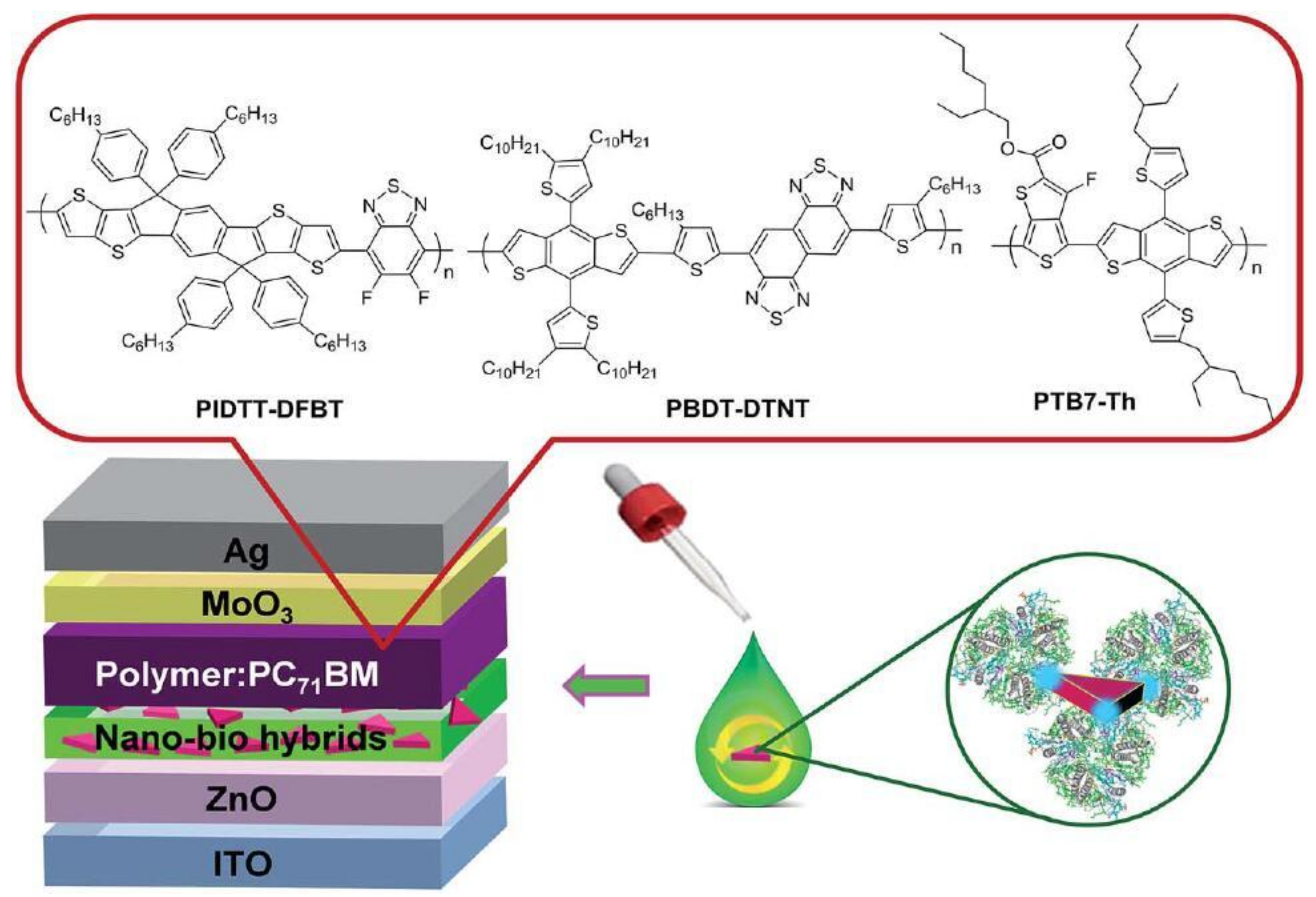
| PTB7:PC71BM/nano-bio hybrid/ZnO/ITO [55] | control Ag prisms-LHCII between the active layer and ETL | LSPR | 16.01 17.99 | 0.79 0.80 | 0.72 0.73 | 9.03 10.57 | ~17% in PCE |
| PBDTTT-C:PC60BM/Au NPs/PEDOT/ITO [78] | control Au NPs ~15 nm between the active and HTL | LSPR | 10.62 11.74 | 0.73 0.73 | 59.9 63.4 | 4.78 5.52 | ~15% in PCE |
| ITO/ZnO/P3HT:PC61BM/MoO3/Al [79] | reference Ag NWs between cathode and ETL Ag NWs between ETL and active layer | LSPR | 8.13 9.87 8.92 | 0.60 0.61 0.60 | 0.62 0.63 0.62 | 3.10 4.05 3.31 | ~31% in PCE |
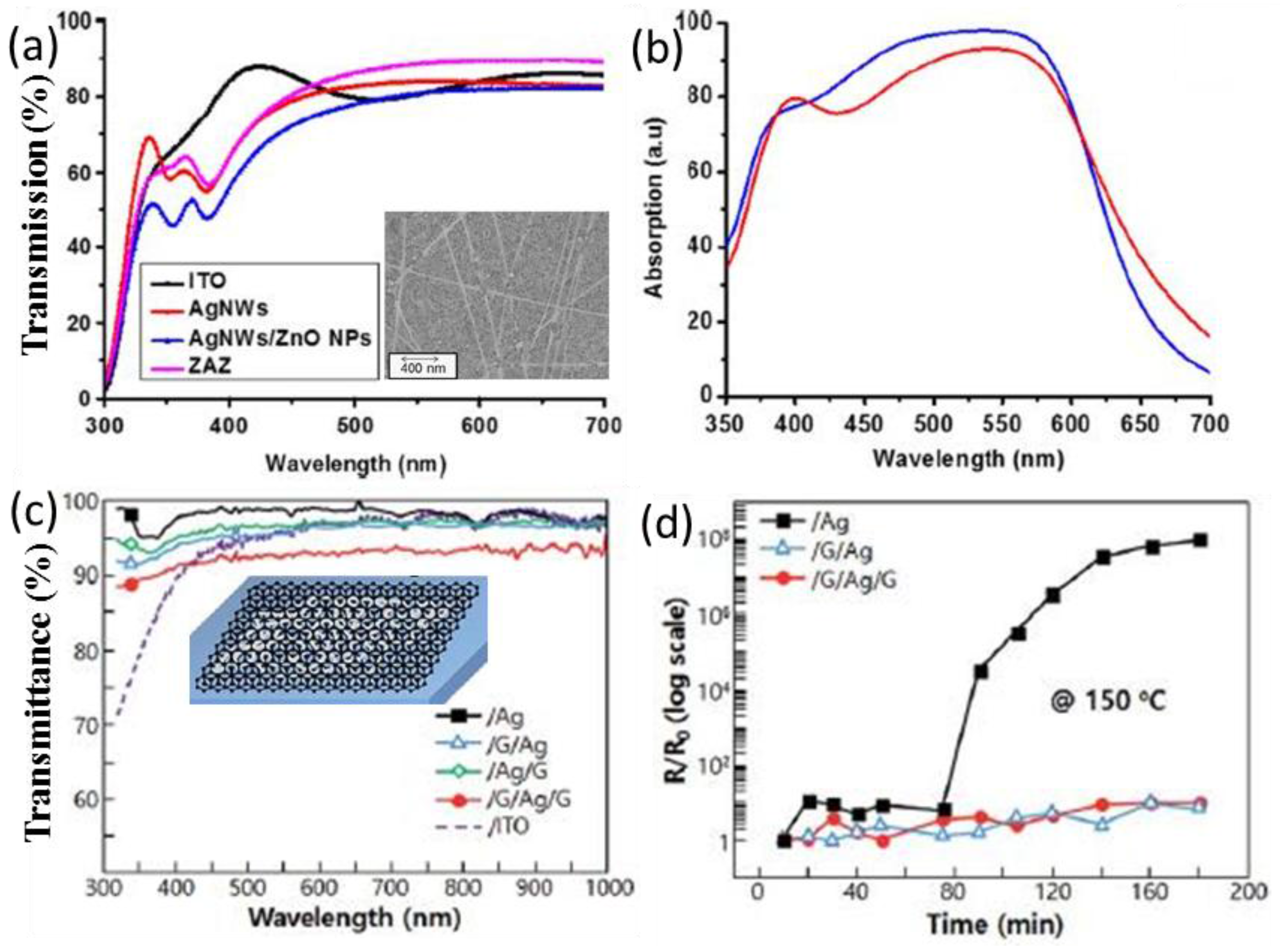
| P3HT:PC61BM/ITO (or ZAZ) [80] | control ZnO/Ag NWs/ZnO as transparent electrode | Higher tranmission above 450 nm | 9.75 11.6 | 0.58 0.54 | 57 57 | 3.16 3.53 | ~12% in PCE |
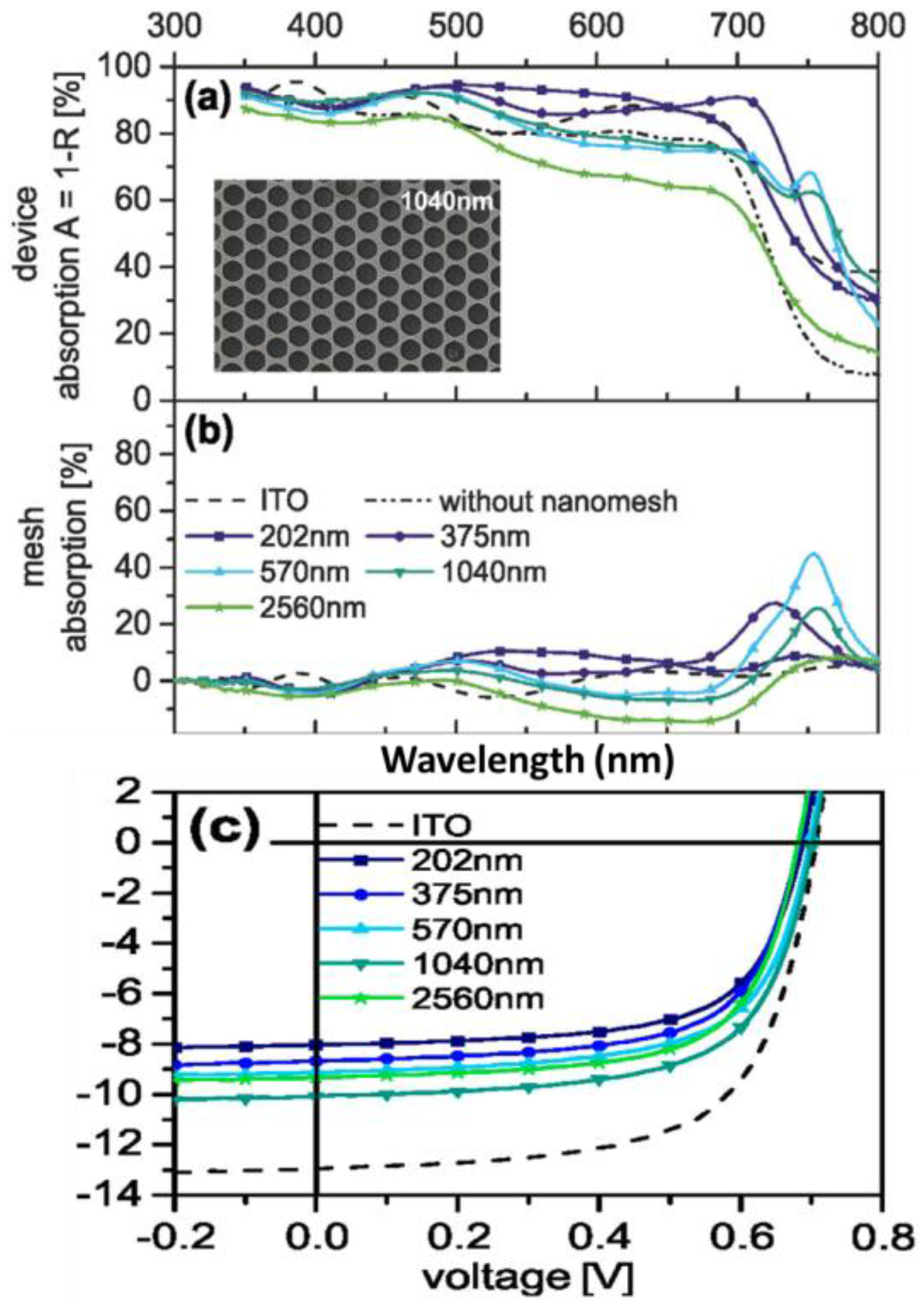
| P3HT:PC61BM/PEDOT/Au (flat or grating) [81] | control Au grating as rear electrode | SPP, photonic waveguide mod | 6.13 6.83 | 0.63 0.63 | 0.59 0.62 | 3.03 3.53 | ~16% in PCE |
| ITO/ZnO/P3HT:PCBM/Ag grating [56] | control Ag grating as rear electrode | SPP, photonic waveguide mode | factor of ca. 5 enhancement of the EQE | ||||
| P3HT:PCBM/Al grating [57] | control Multidiffractive Al grating under light absorbing medium | coupling of SPP modes | absorption in NIR range | ||||
© 2018 by the authors. Licensee MDPI, Basel, Switzerland. This article is an open access article distributed under the terms and conditions of the Creative Commons Attribution (CC BY) license (http://creativecommons.org/licenses/by/4.0/).
Share and Cite
Feng, L.; Niu, M.; Wen, Z.; Hao, X. Recent Advances of Plasmonic Organic Solar Cells: Photophysical Investigations. Polymers 2018, 10, 123. https://doi.org/10.3390/polym10020123
Feng L, Niu M, Wen Z, Hao X. Recent Advances of Plasmonic Organic Solar Cells: Photophysical Investigations. Polymers. 2018; 10(2):123. https://doi.org/10.3390/polym10020123
Chicago/Turabian StyleFeng, Lin, Mengsi Niu, Zhenchuan Wen, and Xiaotao Hao. 2018. "Recent Advances of Plasmonic Organic Solar Cells: Photophysical Investigations" Polymers 10, no. 2: 123. https://doi.org/10.3390/polym10020123
APA StyleFeng, L., Niu, M., Wen, Z., & Hao, X. (2018). Recent Advances of Plasmonic Organic Solar Cells: Photophysical Investigations. Polymers, 10(2), 123. https://doi.org/10.3390/polym10020123