Article

Ferroelectric Self-Poling in GeTe Films and Crystals

1
Max Planck Institute for Chemical Physics of Solids, 01187 Dresden, Germany
2
Department of Condensed Matter Physics, Faculty of Mathematics and Physics, Charles University, 121 16 Praha 2, Czech Republic
3
Institut für Halbleiter-und Festkörperphysik, Johannes Kepler Universität, A-4040 Linz, Austria
4
ESRF—The European Synchrotron, 71 Avenue des Martyrs, 38000 Grenoble, France & Leibniz-Institut für Kristallzüchtung, Max Born Str. 2, 12489 Berlin, Germany
5
DECTRIS Ltd., 5405 Baden-Daettwil, Switzerland
6
Paul Scherrer Institut, Electron Microscopy Facility, 5232 Villigen PSI, Switzerland
7
Partnership for Soft Condensed Matter (PSCM), ESRF—The European Synchrotron, 38043 Grenoble, France
8
Institute of Physics, Ecole Polytechnique Fédérale de Lausanne, 1015 Lausanne, Switzerland
9
CEITEC—Central European Institute of Technology, Masaryk University, Kotlářská 2, 611 37 Brno, Czech Republic
10
Photon Science Division, Paul Scherrer Institut, 5232 Villigen PSI, Switzerland
*
Author to whom correspondence should be addressed.
Crystals 2019, 9(7), 335; https://doi.org/10.3390/cryst9070335
Submission received: 30 May 2019 / Revised: 21 June 2019 / Accepted: 24 June 2019 / Published: 28 June 2019
(This article belongs to the Special Issue Recent Advances in Novel Topological Materials)

Abstract

:
Ferroelectric materials are used in actuators or sensors because of their non-volatile macroscopic electric polarization. GeTe is the simplest known diatomic ferroelectric endowed with exceedingly complex physics related to its crystalline, amorphous, thermoelectric, and—fairly recently discovered—topological properties, making the material potentially interesting for spintronics applications. Typically, ferroelectric materials possess random oriented domains that need poling to achieve macroscopic polarization. By using X-ray absorption fine structure spectroscopy complemented with anomalous diffraction and piezo-response force microscopy, we investigated the bulk ferroelectric structure of GeTe crystals and thin films. Both feature multi-domain structures in the form of oblique domains for films and domain colonies inside crystals. Despite these multi-domain structures which are expected to randomize the polarization direction, our experimental results show that at room temperature there is a preferential ferroelectric order remarkably consistent with theoretical predictions from ideal GeTe crystals. This robust self-poled state has high piezoelectricity and additional poling reveals persistent memory effects.

1. Introduction

In the past decade, a lively interest has been sparked in relation to condensed matter systems with unconventional electronic structures possessing massless Dirac fermions, i.e., systems with a linearly dispersing “Dirac cone” in their band structure. This property is at the heart of a new class of materials called topological insulators [1,2], possibly interesting for technological applications in low power electronics. Their characteristic two-dimensional (2D) energy momentum relation, or band structure, is similar to the graphene model system and their spin texture was studied in surface derived states for numerous materials [3]. For these systems, the strong spin-orbit interaction (SOI) is responsible for topologically non-trivial states with an insulating bulk and protected surface conductivity. Alternatively, SOI can lead to a momentum dependent lifting of the spin-degeneracy and a topologically trivial Rashba-type band structure in materials which lack inversion symmetry [4]. For example, ferroelectric (FE) materials with naturally broken inversion symmetry and large SOI are good candidates for displaying such spin properties. Recently, α -GeTe(111) was predicted to satisfy these criteria by theory [5] which has afterwards been experimentally confirmed using spin- and angle-resolved photoemission measurements [6,7,8,9]. Thus, despite α -GeTe being the simplest possible diatomic ferroelectric known for decades [10], it became a hallmark for a novel class of topologically trivial materials—the so-called ferroelectric Rashba semiconductors.
GeTe has a high critical ferroelectric ordering temperature T C of more than 700 K. A rhombohedral-cubic transformation occurs between 370 C and 430 C [11,12,13], resulting in a non-centrosymmetric space group R3m ( C 3 v 5 ) [12], which is the ferroelectric structure. The common understanding is that the driving force for this displacive off-center distortion in GeTe relies on stereochemical activity of the Te atoms with unused lone-pair orbitals [14,15]. Lone-pair orbitals are also at the heart of the resonance bonding mechanism between crystalline and amorphous state of GeTe, which enables the GeTe ferroelectric switching [16], thus placing GeTe also into the class of phase-change materials [17,18]. GeTe is also studied in the context of thermoelectric materials where figure of merit z T of up to 1 can be achieved, which can even be increased by alloying [19,20].
Interestingly, by alloying with Mn, (GeMn)Te maintains the rhombohedral lattice distortion structure and FE properties up to Mn concentrations as high as 30% [13,21]. In agreement with the crystal symmetry, both GeTe and (GeMn)Te display a 3D Rashba-type electronic structure. Moreover, the magnetic impurities open up a Zeeman gap at the Dirac point, making this the first 3D system to possess a Rashba–Zeeman type spin splitting with clear multiferroic hysteretic properties [9,22]. State-of-the-art operando spin-resolved photoemission results from Ge 0.87 Mn 0.13 Te showed that manipulation of both the Rashba and magnetic spin polarization upon switching of the ferroelectric polarization is possible, thereby demonstrating a strong magnetoelectric coupling with magnetoelectic functionality entangled with the Rashba-type spin texture [23].
It turns out that the large ferroelectric lattice distortion in α -GeTe is also the most significant ingredient for the giant Rashba-type spin-splitting [24], and, to this date, it is one of the largest observed at a valence-band maximum (≈4.2 eVÅ [6]). In other words, the presence of large SOI in α -GeTe, so ubiquitous to many system with broken inversion symmetry, is not the primary cause for the anomalously high Rashba-strength parameter, but instead is due to significant structural distortion of α -GeTe(111) along the rhombohedral c-axis [25]. Therefore, in this contribution, we provide further experimental evidence of the rhombohedral lattice distortion in α -GeTe. By using EXAFS and anomalous scanning X-ray diffraction techniques, complemented with piezoresponse force microscopy (PFM), we show that GeTe possesses a robust ferroelectric self-polarized state. To the best of our knowledge, this aspect of α -GeTe ferroelectric properties was elusive in the first PFM studies from α -GeTe [14] because they were performed on a factor 10 thinner films compared to our samples [6], and did not manifest the self-poling. In this context, a comprehensive comparison of FE domain structures between millimeter sized crystals grown with chemical vapor deposition (CVD) and 200 nm thin films grown by molecular beam epitaxy (MBE) are presented in order to provide further evidence on the GeTe self-poled state.

2. Materials and Methods

2.1. Crystal and Thin Film Growth

Millimeter-sized GeTe crystals were grown from the vapour phase by dissociative sublimation and by chemical transport with Germanium(IV) iodide (GeI4) as transport agents in sealed ampules. High quality epitaxial 200-nm-thick-ferroelectric thin films of Te-terminated α -GeTe were grown by MBE using GeTe and Te sources, following the procedures described in Ref. [26]. In the present work, however, Zn-doped InP(111)A substrates were used instead of BaF 2 (111) in order to be able to apply a voltage across the GeTe films using the conducting InP substrates as a back gate. Prior to GeTe growth, the oxide of the InP substrate was desorbed at about 460 C as checked by reflection high-energy electron diffraction (RHEED). Subsequently, GeTe was deposited at a growth rate of 2 Å/s and substrate temperature of 300 C at which two-dimensional (2D) growth occurs as evidenced by the streaked RHEED patterns observed throughout the whole growth process. In some cases, the GeTe film surface was protected by a stack of thin amorphous tellurium and selenium capping layers which were deposited after growth and cool down to room temperature. This cap was completely removed by annealing in vacuum before further measurements. The material was inspected with scanning electron microscopy (SEM) and then prepared for transmission electron microscopy (TEM) by the focused ion beam technique in a FIB/SEM (Zeiss NVision 40, Carl Zeiss Microscopy GmbH, Jena, Germany). For the TEM investigation, a JEM F200 TEM (JEOL Ltd., Tokyo, Japan) operated at 200 kV was used.

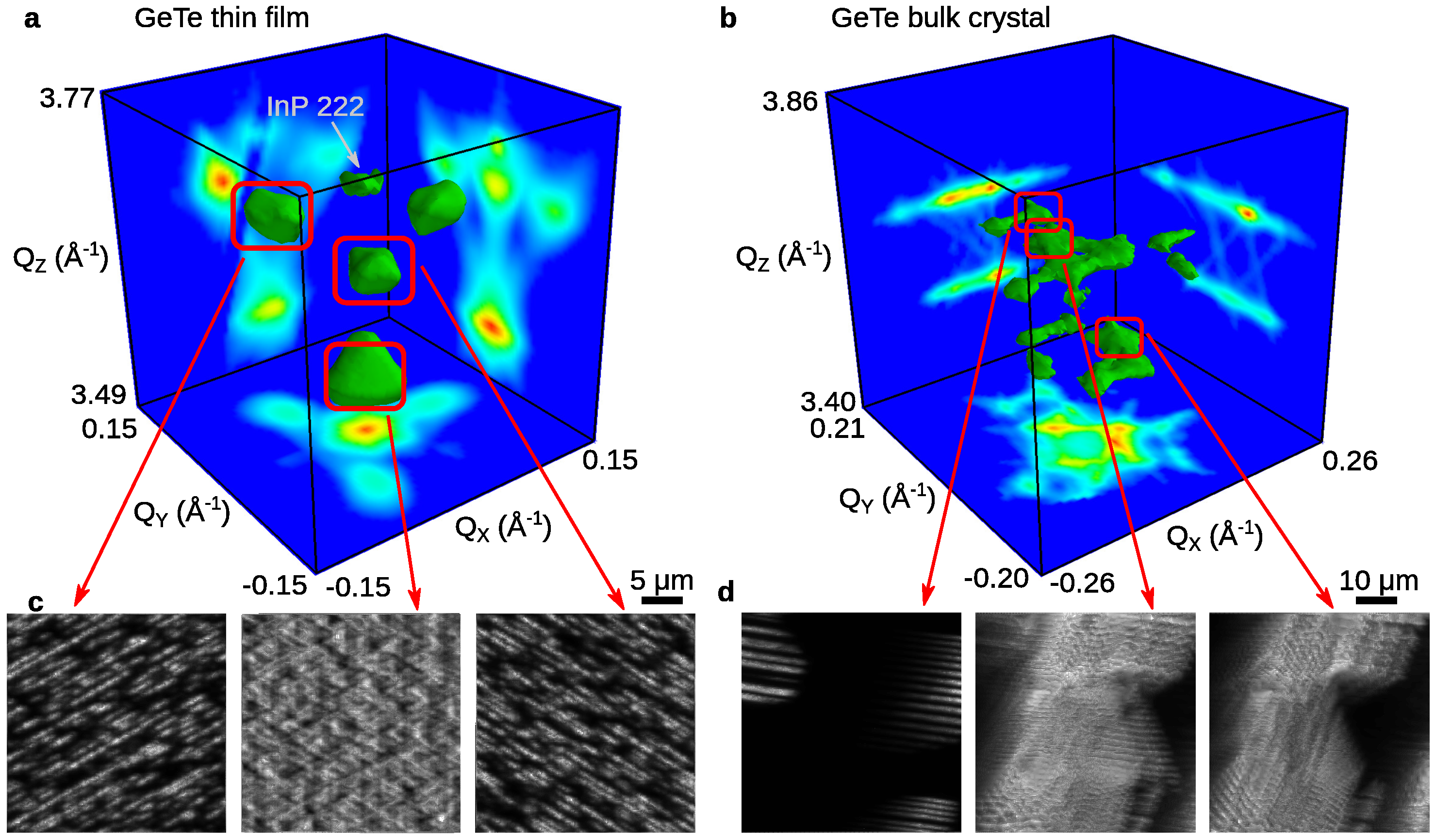
2.2. Scanning X-Ray Diffraction

A nano-focused synchrotron X-ray beam at beamline ID01 at the European Synchrotron Radiation Source Facility (ESRF) in Grenoble, France, with an energy of 11.05 keV was used to record the spatial distribution of diffracted intensity. The X-ray beam was focused using a pair of Kirkpatrick–Baez mirrors operated in con-focal geometry leading to a full width at half maximum beam size of 220 nm × 220 nm. Using a piezo-driven sample stage, we scanned the sample through this pencil-like X-ray beam whilst simultaneously recording the Bragg diffracted intensity with an area detector operated at a frame rate of up to 100 fps. The angular resolution was defined by a sample to detector distance of 530 mm and the 55 μ m pitch of the 516 × 516 detector pixels. This procedure results in a 2D position dependent mapping of the diffracted intensity as described in detail by Chahine et al. [27] and was previously successfully applied to thin layers and nanostructures [28,29,30,31,32]. Employing an additional sample rotation, a five-dimensional data set I ( x , y , Q x , Q y , Q z ) , comprising two real space and three reciprocal space coordinates, is obtained. Note that the absorption depth of X-rays for the used energy in GeTe is around 20 μ m, making this method bulk sensitive. For the presented studies, we recorded the diffraction intensity in the vicinity of the 222 and 444 Bragg reflections. Note that all specified Miller indices refer to the rhombohedrally distorted unit cell derived from the rock–salt structure. Considering the (111) facet/surface of the studied bulk crystal and thin film samples, this corresponds to an incidence angle of around 18 and 39 to the surface. This results in beam footprints of around 700 nm or 350 nm × 220 nm on the sample’s surface, respectively.

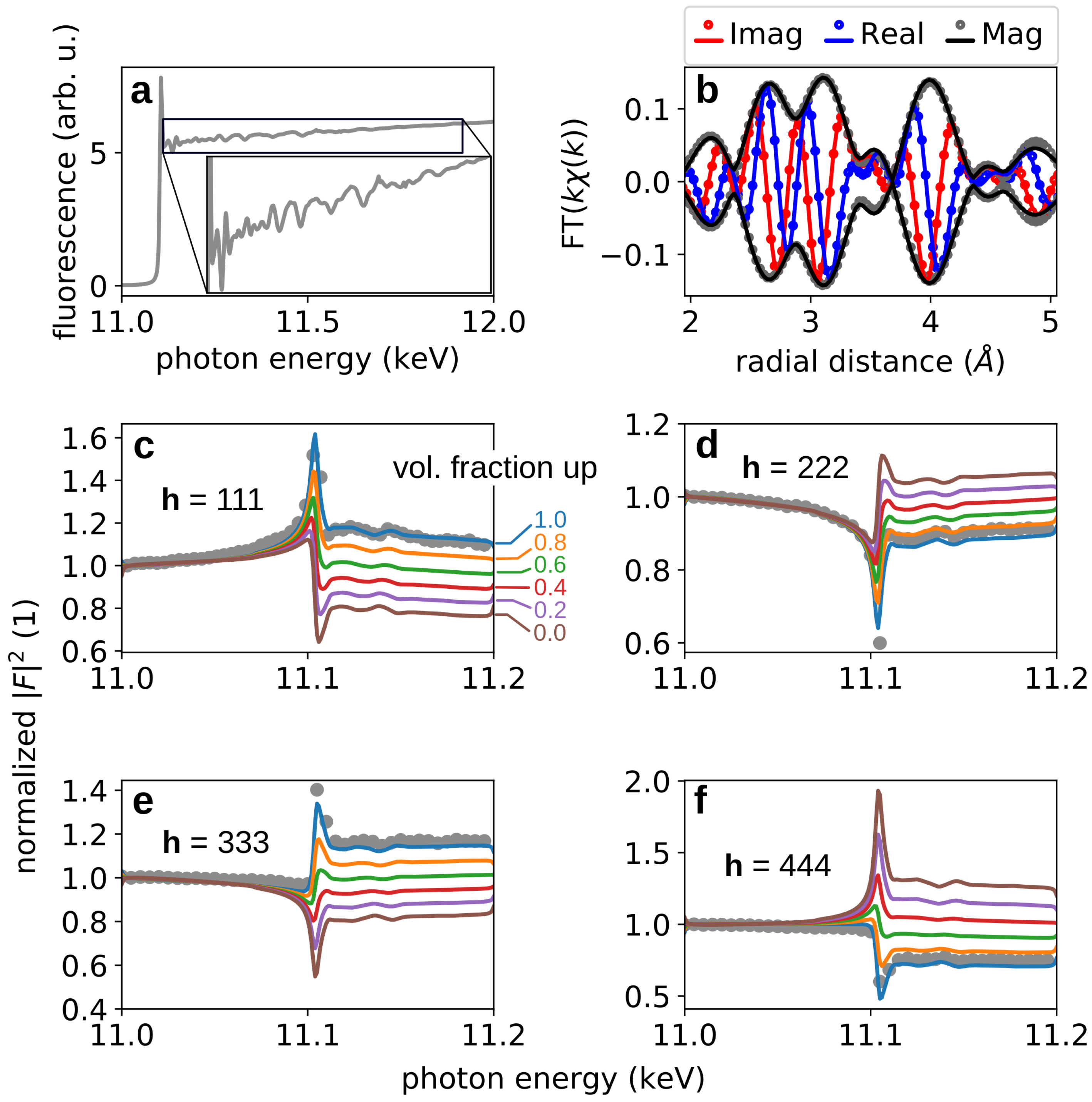
2.3. X-Ray Absorption Fine Structure Spectroscopy and Anomalous Diffraction

Extended X-ray absorption fine structure measurements (EXAFS) were carried out at the XAS beamline at the Synchrotron Light Source ANKA in Karlsruhe, Germany. Data were acquired at the Ge-K edge in fluorescence mode. The obtained spectra were analyzed using Artemis [33] and Mkfit [34], which calculate the EXAFS signal using an ab initio multiple scattering theory. The combination of the mentioned software packages allows for directly refining the unit cell structure of GeTe together with the position of the atoms inside the unit cell. In contrast, Artemis alone only allows for refining the coordination shell radii. Anomalous diffraction was performed at beamline ID01 at the ESRF around the Ge-K edge in symmetric coplanar diffraction geometry. Using a photon energy close to the electronic transition, the diffracted intensity can reveal the ferroelectric polarization [35,36]. For our anomalous diffraction measurements, a monochromatic beam with an energy varied from 11.0 to 11.2 keV and beam size of 200 μ m × 200 μ m was used.
The energy dependencies of the intensities for diffractions h = 111 , 222 , 333 , 444 have been calculated using the kinematical approximation [37]. In σ -polarization, the integrated intensity of the symmetrical diffraction is
J h ( E ) = A I inc ( E ) F ( h , E ) E 3 sin 2 ( Θ B ) cos ( Θ B ) 1 Im ( Q z ) 1 e 2 Im ( Q z ) T ,
where A is a scaling constant, I inc ( E ) is the (energy dependent) intensity of the primary beam, Θ B is the energy dependent Bragg angle, and T is the layer thickness. We denoted Q = K f K i as the scattering vector inside the diffracting crystal including refraction and absorption (the difference of the wave vectors of the scattered ( K f ) and transmitted waves ( K i )). Its vertical (z) component is complex due to absorption and its imaginary part is
Im ( Q z ) = 4 π λ Im ( n ) sin ( Θ B ) ,
where λ 1 / E is the photon wavelength, and n ( E ) = 1 δ ( E ) + i β ( E ) is the energy dependent complex refraction index of the layer material. Close to the ionization energies, Im ( Q z ) exhibits a step-like increase (absorption edge), which results in a sudden decrease of the X-ray penetration depth.
The most important quantity in the expression of the integrated intensity is the GeTe structure factor F ( h , E ) in the diffraction maximum Q = h
F ( h , E ) = f Ge ( h , E ) r Ge e i h . ( r Ge + d ) + f Te ( h , E ) r Te e i h . r Te ,
where f Ge , Te ( h , E ) are the energy dependent atomic form factors of Ge and Te, r Ge , Te are the positions of Ge and Te in the unit cell of the rocksalt lattice, and d is the relative displacement of the Ge atoms from the central position taken in the rocksalt structure. Here, h represents the three-dimensional, reciprocal lattice vector of the respective Bragg reflection.
In the simulation, we use the well-known approximation of the Thomson (classical) form factors by a sum of four Gaussians [38]. The energy dependent dispersion (Hönl) corrections f ( 1 ) ( E ) + i f ( 2 ) ( E ) can be decomposed into a smooth part related to the isolated atom and an oscillatory part (the fine structure) that depends on the chemical environment of the atom and becomes important close to its absorption edges. Since there is only one unique resonant atom in the crystal structure, the imaginary part f ( 2 ) can be directly extracted from the EXAFS data. The smooth parts of f ( 1 ) and f ( 2 ) can be taken from databases [39,40]. The fine structure for f ( 1 ) was then obtained using the Kramers–Kronig relations applied to the spectra of f ( 2 ) ( E ) [41]. Finally, the simulated energy dependence was convoluted with the energy resolution function, for which we used a Lorentzian function with the full width at half maximum of 1 eV.

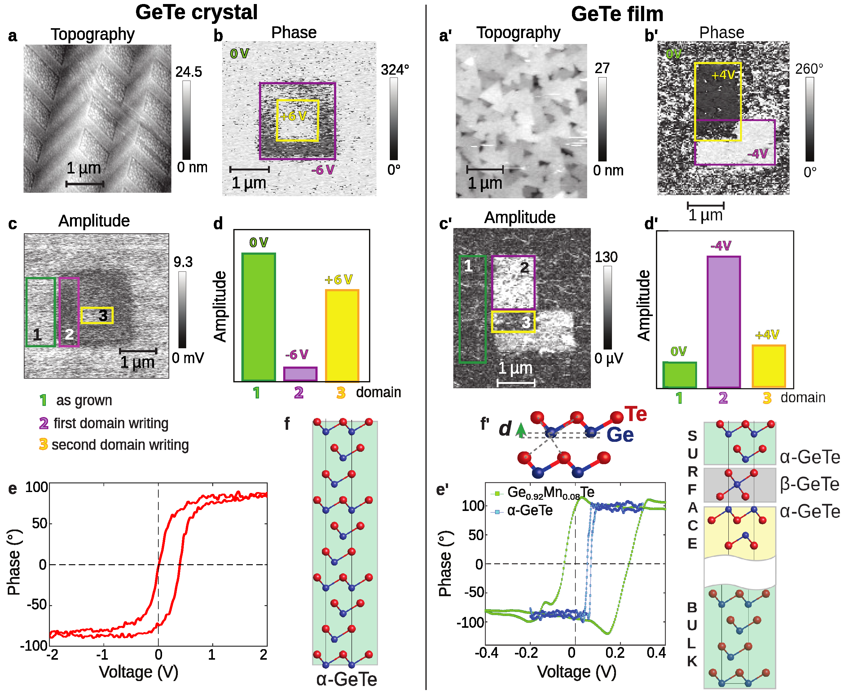
2.4. FE Domains Probed by Piezo-Force Scanning Microscopy

Piezoresponse force microscopy (PFM) was used to characterize the ferroelectric properties of the near surface region [42], but typically accounts for material bulk properties down to ≈100 nm. The PFM measurements were performed at the Swiss Light Source NanoXAS beamline [43]. In this technique, the piezoelectric effect causes a mechanical response to an excitation of the sample via an AC voltage applied between the sample and the probe tip. The induced response of the cantilever deflection, which is detected using a lock-in technique, translates to FE domain properties with characteristic amplitude and phase signals: the first is a measure for the absolute magnitude of polarization, whereas the second corresponds to the polarization direction. In our case, the PFM amplitude signal is proportional to the projection of the FE polarization perpendicular to the sample surface. Therefore, it is proportional to the strength of spontaneous polarization along the α -GeTe(111) surface normal.
In addition to simultaneous mapping of sample topography and FE amplitude and phase, local spectroscopy can be recorded; i.e., the response of the PFM signal to poling. This enables measuring hysteresis loops, where our data systematically show asymmetric P–E loops and data from films on InP(111) show coercive fields less than 10 mV. In light of this small coercive field, we note that the PFM-phase domain mapping on films remains unchanged even after two days, thus ruling out charging artifacts induced by the PFM setup. For a sufficient signal-to-noise ratio in data acquisition, the excitation during PFM measurement was higher for bulk crystals (4V) than for thin films (1V), both with frequencies around 270 kHz.
Although PFM is measured close to resonance, no cross-talk with topography is visible which validates the quality of our PFM data discussed below. In order to ensure consistency, the PFM characterization of our GeTe films was compared to data obtained with a Cypher AFM from Asylum Research at the PSCM AFM Laboratory at the ESRF. The P–E loops were measured in dual AC resonance tracking. It follows that both instrumental setups deliver consistent results, in agreement with published results [6,7,23].

3. Results and Discussion

We start the characterization of the bulk crystals by discussing scanning electron microscopy. Figure 1a,b displays the investigated GeTe bulk crystal showing typical faceting, as expected for the slightly rhombohedrally distorted rock salt crystal structure, with pronounced (111) and (001) facets. When zooming in on the (111) facets (Figure 1c “SEM surface”), a clear contrast pattern appears which we associate with the ferroelectric domains which typically arrange in the observed herringbone pattern [44,45]. The edges of the domains on the surface of the crystal are typically aligned parallel or perpendicular to the corners of the respective (111) facet, i.e., along a 11 2 ¯ or a 1 1 ¯ 0 direction. In contrast to the (111) facets, no contrast associated with the domain pattern can be detected on the (100) facets (Figure 1d). In order to study how the domains propagate into the depth of the crystal, lamellae were cut by a focused ion beam. A transmission electron micrograph of a cross sectional lamella labelled “TEM bulk” is shown in Figure 1e and shows that the domain pattern from the surface propagates only around 1 μ m into the crystal before it changes. Deeper inside the material, domains with various orientations are found.
From the electron micrographs, it is not a priori clear what the polarization axis in the specific domains is. Since it is well established that the FE polarization axis is defined by the distortion axis of the rhombohedral crystal distortion [12,13], X-ray diffraction can be used to determine the polarization axis. In Figure 2, scanning X-ray diffraction data are shown for GeTe bulk crystal and thin film samples. Panels (a) and (b) show three-dimensional reciprocal space maps of the GeTe 222 Bragg peak. The data are obtained using a nano-focused X-ray beam, however, shown here is the sum obtained from data collected over an area of 20 μ m × 20 μ m and 40 μ m × 40 μ m for the thin film and bulk crystal, respectively. Multiple peaks of GeTe originate from rhombohedral distorted domains showing a different distortion axis with respect to the crystal surface. Since both the bulk crystal and thin film were measured on a (111) surface, the 111 distortion axes are either nearly perpendicular to this surface or enclose an angle of roughly 70 . This results in two groups of diffraction peaks which show up at lower momentum transfer (increased lattice spacing perpendicular to the surface) or higher momentum transfer (decreased lattice spacing). For the epitaxial thin film, the substrate induces a preference for the domains with distortion axis along the (111) surface normal seen by the fact that the peak at the lowest Q z position is the strongest one. In agreement with earlier studies [6,46], three additional peaks appear which correspond to domains which have the distortion axis along one of the oblique 111 directions of the substrate. On the other hand, for the bulk crystal, where no reference crystal enforces a particular orientation of the domains with respect to each other, the reciprocal space maps are more complicated and even the domains at lower Q-position split into multiple peaks.
The real space distribution of the various domains is obtained from the scanning X-ray diffraction data by taking the real space map of certain features identified in the cumulative reciprocal space maps shown in Figure 2a,b. Examples of such real space maps are shown in Figure 2c,d. For the thin film data, this confirms that the majority domain is indeed the one with the distortion axis along the (111) surface normal. This domain is present everywhere in the film and only interrupted by stripe like domains with oblique distortion axis. For the bulk crystal, the situation is again more complicated since information is collected from a large volume penetrated by the X-ray beam along its propagation direction. Thus, the obtained resolution depends not only on the beam size but also on the extinction/absorption lengths. As for the thin films, stripe like domains with various orientations can be found. Depending on the location on the single crystal, some types of domains are completely absent. The herringbone domain pattern found in Figure 1 with characteristic domain size below 1 μ m can be seen in parts of the right two panels in Figure 2d, but the resolution is not sufficient to completely resolve it. Since these two panels correspond to one set of domains with distortion direction perpendicular to the surface and one with an oblique distortion axis, this indicates that the near surface region of the bulk material consists of a mixture of ferroelectric polarization axes.
The presented scanning X-ray diffraction data are sensitive only to the distortion axis, but can not clarify the sense of ferroelectric polarization or the amount of the ferroelectric polarization. For that purpose, we employed anomalous diffraction as well as EXAFS. EXAFS is sensitive to the atomic distances around the atom where a core hole is produced by the absorption of an X-ray photon. Equivalent to previous studies [6,13], we have used this technique to determine the displacement of the Ge sublattice from the center of the surrounding Te atoms from data shown in Figure 3a,b.
The value of the displacement is an important input parameter for the analysis of the anomalous diffraction data presented in Figure 3c–f. However, the anomalous diffraction signal depends also on the sense of the displacement. Figure 3c–f shows the normalized diffracted intensity of the Bragg peaks h = 111 , 222 , 333 , 444 for energies near the Ge-K edge (∼11.1 keV). We limit this analysis to the majority domains in the thin film samples, i.e., those with out of plane distortion axis. For this reason, we performed calculations of the energy dependencies of the Bragg intensity (as described in Section 2.3) for all symmetrical diffractions with the displacement vector d of the Ge sublattice being parallel to the normal of the (111) sample surface. We assume that the contribution of both states add up incoherently—as a sum of intensities weighted by their volume fraction. Hence, we neglect possible interference of the waves diffracted from various domains. We found that the shape of the resulting energy dependence at the Ge-K absorption edge sensitively depends on d and on the volume fraction of the “up” and “down” domains.
In Figure 3c–f, we compare the measured energy dependencies of the diffracted intensities with simulations performed for varying volume fraction of up and down domains at a constant displacement magnitude of d = 0.3 Å as determined by EXAFS. In all diffractions, the best correspondence was achieved assuming that all domains have the displacement d of the Ge sublattice parallel to the outer surface normal [111] (“up” domains). Repeating the simulations for various values of d, we found that d = 0.3 Å indeed gives the best correspondence. The displacement d together with the charge density in the unit cell can also be used to estimate the polarization of ferroelectric GeTe. Polatoglou et al. [47] have shown that, like this, a dipole moment of 1.4 D per primitive unit cell can be obtained. This corresponds to a polarization of roughly 5 μ C/cm 2 . From our measurements, we conclude that, in the probed area of several 100 μ m 2 , despite the fact that α -GeTe possesses inhomogeneous polarization in three dimensions, there is a strong preference for one polarity of the ferroelectric polarization, which we associate with a self-polarized state.

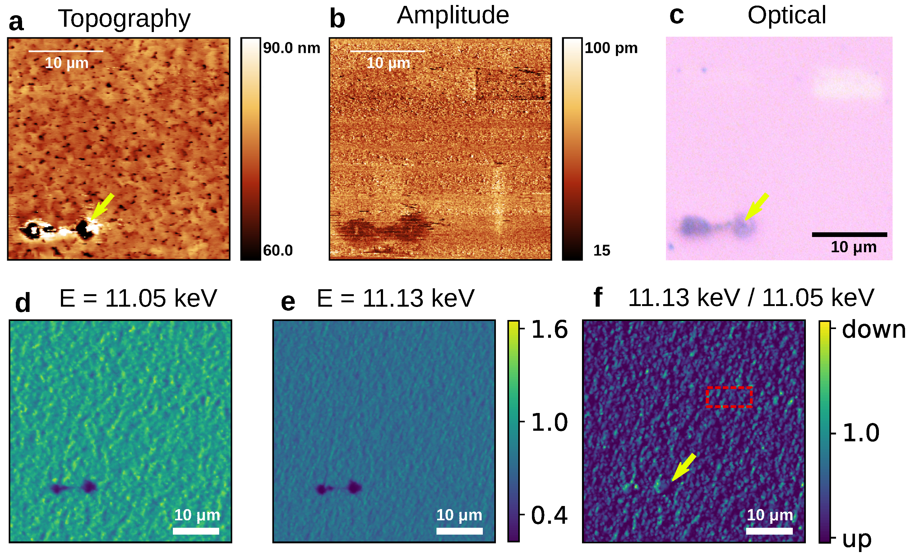
3.1. Self-Polarized State

To further investigate this self-polarized state, we compare the EXAFS and anomalous diffraction results with PFM. Generally speaking, a significant piezoelectric response in ferroelectrics occurs after poling and disappears upon heating above T C . In our case, the α -GeTe near surface region shows pronounced piezoelectricity without prior poling processes. Figure 4 compares the self-poled states between bulk crystal and thin film in panels (a–e) and (a′–e′), respectively.
We first discuss the data of PFM domain writing, seen in panels (b–d) and (b′–d′), respectively. For qualitative comparison of FE order between bulk crystal and thin film, panels (a,a′) show the sample topography, on top of which we wrote FE domains. Panels (b,b′) show the phase, and (c,c′) the amplitude signal from the written domains. Data are compared from three areas: pristine area 1 (green), domain 2 written with negative voltage (magenta), and twice-written domain 3 indicated in yellow. For a quantitative comparison of the FE strength inside written domains, panels (d,d′) show the average amplitude signal from selected areas. We note that data obtained from the GeTe crystal and from the film are different. While topography from the crystal is displaying the well-known herringbone FE-domain structure [44], the films show triangular facets with characteristic sizes from 200 to 800 nm, possibly related to twinned domains rotated by 60 [26,46]. The most striking differences, however, are found in the PFM signals. More specifically, we note that the self-poling measured on pristine unpoled areas, indicated by area 1 in panels (c,c′), is much stronger for the crystal. Writing a FE domain in the opposite direction with −6 V (magenta frame in c) on the crystal is possible, the related phase change around 180 in (b) confirms the domain writing, but the related amplitude signal seen in (d) is significantly weaker compared to the pristine state. By rewriting the domain with +6 V (yellow area), the amplitude signal increases significantly, which is firm evidence that self-poling is favoring an upward polarization. Executing the same domain writing protocol for films (panels (b′–d′)) we note that the overall poling kinematic behavior is exactly opposite. This experimental observation, however, is at odds with hysteresis data in local contact mode seen in panels (e,e′), where both crystal and film show consistent asymmetric shifts to the positive side of the electric field axis. In order to demonstrate that this is a real ferroelectric response not dominated by electrostatic artifacts, the data are cross-compared with data obtained from GeTe alloyed with 8% Mn, which also shows asymmetric P–E loops, but with larger coercive field, similar to data presented in Ref. [7] from 32 nm thick α -GeTe films grown on Si(111). This means that the self-poling can probably be tuned by strain effects induced by various substrates and film thicknesses. Another possibility is, for example, to use Mn-alloying because the system gradually change to the non-ferroelectric cubic structure [21]. Before addressing the above conundrum, we first discuss the ferroelectric origin of the observed asymmetric hysteresis shift, which is strikingly different from typical ferroelectrics.
According to Spaldin [15], there are two possible physical origins for the mandatory non-centrosymmetric distortions needed for ferroelectricity. They are representative for perovskites or for group IV chalcogenides such as GeTe. For perovskites, it is the ligand-field stabilization, and for GeTe it is the already mentioned stereochemical activity of the lone pairs. For example, in PZT, self-poling effects with the hysteresis shifted to the positive side can be enabled by domain pinning induced by defects [48], oxygen vacancies [49], or the system can also be naturally polarized [50]. On the other hand, for the room temperature multiferroic BiFeO 3 , a downward self-poling, i.e., the hysteresis is shifted to the negative side, can be achieved by temperature gradients [51]. For GeTe, there is no need to “engineer” the self-poling because of the intrinsic non-centrosymmetric rhombohedral structure, in which an electric dipole is formed due to a relative Ge-Te sublattice displacement along the (111) direction, as schematically depicted by the green arrow in Figure 4f. It turns out that this Te-terminated surface arrangement is also thermodynamically more favorable [25].

3.2. Self-Poling of GeTe Surface Versus Bulk

The domain structure in the near surface region in our crystals and films is certainly different, which is evident from the different surface topographies as seen in Figure 4a,a′. It turns out that the crystal surface seen in the micrographs of Figure 1 was not suitable for AFM/PFM measurements. Furthermore, the crystals cannot be cleaved (GeTe has no natural cleavage plane), and are too soft (ductile) to crack at room temperature. For this reason, data seen in Figure 4a–c were measured from a surface obtained by cracking the GeTe crystal at ≈22 K by using a knife-edge holder. We managed to crack the surface along the (111) plane because, as seen in Figure 1, this is the only crystallographic orientation in which the herringbone domain structure can be observed (see Figure 4a). In agreement with our earlier angle-resolved photoemission studies from GeTe films [6], the cracked surface was Te-terminated, as schematically depicted in the simplified model in Figure 4f. On the other hand, the GeTe surface from films had a protective Te and Se cap, which was removed by annealing at 270 C . The resulting surface relaxation depicted in Figure 4f′ was found to be consistent between photoemission experiments and related theoretical simulations [6,22,23,25].
Briefly said, the film surface is Te-terminated, with a surface relaxation that induces a sub-surface FE domain wall similar to the rock-salt β -GeTe crystal structure denoted in grey in Figure 4f′. Underneath this domain wall, another α -GeTe domain is formed with opposite stacking of the GeTe triple-layers. Because our bulk sensitive EXAFS and diffractions studies unambiguously show that the Ge sublattice is shifted upward as depicted in Figure 4f, underneath this surface/sub-surface region, the film-bulk is depicted with GeTe triple-layers having the same upward Ge shift.
As already mentioned, our PFM analysis in Figure 4 suggests that both crystals and films have consistent self-poling in hysteresis, but opposite domain mapping characteristics. Our understanding is that PFM domain mapping for GeTe is sensitive to interfacial effects near the film surface (1–100 nm), whereas the local piezoelectric response is bulk sensitive (>100 nm) for both the crystal and film. More experimental studies are needed to elucidate to which extent PFM domain writing affects GeTe bulk properties. However, a direct piece of evidence of the interfacial effects in our films is seen in Figure 4: the amplitude signal of the self-poled state (pristine region) is a factor 70 stronger for crystals (9 mV vs. 130 μ V). Therefore, a possible explanation for the striking difference in domain mapping between crystal and film is that in local contact mode the surface excitation is different compared to domain mapping: in the first case, the cantilever is fixed in position; in the latter, it is sweeping the surface. It turns out that for “leaky” ferroelectrics, i.e., those with significant electric conductivity such as our slightly p-doped GeTe, heat and pulsed currents are essential ingredients in manipulating the FE domains [52]. Therefore, it is reasonable to assume that a DC voltage applied to the cantilever in local contact mode, combined with pulsed currents induced by AC voltage, are sufficient to reorient the surface-interface FE domain structure depicted in Figure 4f′ such that the hysteresis is consistent with data obtained from the crystal.
To further corroborate this picture, we performed XRD measurements inside and outside the domains written by PFM. Corresponding data are shown in Figure 5. A defect was used as a marker to ensure that the same sample area was investigated by all methods. Figure 5a–c show the AFM topography and PFM amplitude as well as an optical microscope image, confirming that a domain was written by PFM. Exactly inside this location, scanning XRD imaging was performed at two energies close to the Ge-K edge at the 444 Bragg reflection (Figure 5d,e). According to Figure 3c–f, the ratio of intensity above and below the Ge-K edge is sensitive to the ferroelectric polarization. Figure 5f shows this ratio, which in the majority of the scanned area is smaller than 1, thereby indicating that the ferroelectric polarization is pointing upwards. The FE domain written by PFM, however, cannot be identified in any of the scanning XRD data. We note that, for measurements in Figure 5, the sample is illuminated with an X-ray photon beam with up to 10 10 photons/s in the focal spot with FWHM of 220 × 220 nm, which remains on one sample spot for 10 msec.
Finally, we discuss a possible impact of the X-ray beam on the measured ferroelectric state. Because GeTe is a p-doped semiconductor in a self-poled stated, and the sample is grounded, we cannot exclude that the photon beam influences the ferroelectric state by creating a charge gradient. Consequently, the associated Coulomb field could influence the GeTe FE polarization. Although a strong light beam was shown to have the potential to influence ferroelectricity [53,54], we highlight that most of the hard X-rays pass through the film without interaction. From a quantitative viewpoint, the same results were found from the measurement in Figure 3f, which was obtained using more than five orders of magnitude less photon density. We conclude that scanning XRD is sensitive to the full film volume, confirming the strong preference for self-polarization in the up direction. Finally, interfacial effects in the GeTe domain mapping via PFM appear insufficient to manipulate the FE order of the film bulk because, within the experimental resolution, XRD inside and outside written domains delivered identical results.

4. Conclusions

In conclusion, we described the self-polarization effect on unpoled α -GeTe crystal and thin films. We provided further characterization of the α -GeTe multidomain structure in bulk crystals and films. Bulk sensitive EXAFS and anomalous diffraction studies confirmed that the multidomain structure does not randomize the FE order. Instead, α -GeTe features intrinsic self-poling consistent with the rhombohedral distortion in which the Ge atoms are upward shifted by ≈0.3 Å along the direction of the outer surface normal. The discovery of stable room-temperature self-polarization in a “simple” diatomic compound with topological properties opens up a promising path toward robust and programmable semiconductor-based spintronics with memory effects.

Author Contributions

Scanning XRD experiment, D.K., C.R., G.S., and J.K.; EXAFS experiment and data evaluation, D.K.; thin film growth, G.S.; bulk crystal growth: H.B.; anomalous diffraction calculations: V.H., and C.R.; PFM experiments, N.P., G.S., M.C., and J.K.; original draft preparation, D.K., and J.K.; scanning electron microscopy, E.M.; supervised the experimental results, J.H.D.

Funding

This research was funded by the European Regional Development Fund (ERDF) within project CZ.02.1.01/0.0/0.0/15_003/0000485 as well as by the Austrian Science Fund (FWF) within projects J3523-N27 and P30960-N27.

Acknowledgments

The authors acknowledge the support of Alain Panzarella and Diego Pontoni at the PSCM facilities at the ESRF as well as Stefan Mangold at the XAS-beamline at ANKA for their support. Scanning XRD experiments were performed on beamline ID01 at the European Synchrotron Radiation Facility (ESRF), Grenoble, France. As well as Open Access Funding by the Austrian Science Fund (FWF).

Conflicts of Interest

The authors declare no conflict of interest.

References

  1. Moore, J.E. The birth of topological insulators. Nature 2010, 464, 194–198. [Google Scholar] [CrossRef] [PubMed]
  2. Hasan, M.Z.; Kane, C.L. Colloquium:Topological insulators. Rev. Mod. Phys. 2010, 82, 3045–3067. [Google Scholar] [CrossRef]
  3. Dil, J.H. Spin- and angle-resolved photoemission on topological materials. Electron. Struct. 2019, 1, 023001. [Google Scholar] [CrossRef] [Green Version]
  4. Rashba, E.I. Properties of semiconductors with an extremum loop. 1. Cyclotron and combinational resonance in a magnetic field perpendicular to the plane of the loop. Sov. Phys. Solid State 1960, 2, 1109–1122. [Google Scholar]
  5. Di Sante, D.; Barone, P.; Bertacco, R.; Picozzi, S. Electric Control of the Giant Rashba Effect in Bulk GeTe. Adv. Mater. 2013, 25, 509–513. [Google Scholar] [CrossRef] [PubMed]
  6. Krempaský, J.; Volfová, H.; Muff, S.; Pilet, N.; Landolt, G.; Radović, M.; Shi, M.; Kriegner, D.; Holý, V.; Braun, J.; et al. Disentangling bulk and surface Rashba effects in ferroelectric α-GeTe. Phys. Rev. B 2016, 94, 205111. [Google Scholar] [CrossRef]
  7. Liebmann, M.; Rinaldi, C.; Di Sante, D.; Kellner, J.; Pauly, C.; Wang, R.N.; Boschker, J.E.; Giussani, A.; Bertoli, S.; Cantoni, M.; et al. Giant Rashba-Type Spin Splitting in Ferroelectric GeTe(111). Adv. Mater. 2016, 28, 560–565. [Google Scholar] [CrossRef]
  8. Elmers, H.J.; Wallauer, R.; Liebmann, M.; Kellner, J.; Morgenstern, M.; Wang, R.N.; Boschker, J.E.; Calarco, R.; Sánchez-Barriga, J.; Rader, O.; et al. Spin mapping of surface and bulk Rashba states in ferroelectric α-GeTe(111) films. Phys. Rev. B 2016, 94, 201403. [Google Scholar] [CrossRef]
  9. Krempaský, J.; Fanciulli, M.; Pilet, N.; Minár, J.; Khan, W.; Muntwiler, M.; Bertran, F.; Muff, S.; Weber, A.P.; Strocov, V.N.; et al. Spin-resolved electronic structure of ferroelectric α-GeTe and multiferroic Ge1−xMnxTe. J. Phys. Chem. Solids 2019, 128, 237–244. [Google Scholar] [CrossRef]
  10. Pawley, G.S.; Cochran, W.; Cowley, R.A.; Dolling, G. Diatomic Ferroelectrics. Phys. Rev. Lett. 1966, 17, 753–755. [Google Scholar] [CrossRef]
  11. Muir, J.A.; Beato, V. Phase transformations in the system GeSe-GeTe. J. Less Common Met. 1973, 33, 333–340. [Google Scholar] [CrossRef]
  12. Chattopadhyay, T.; Boucherle, J.X.; von Schnering, H.G. Neutron diffraction study on the structural phase transition in GeTe. J. Phys. C Solid State Phys. 1987, 20, 1431–1440. [Google Scholar] [CrossRef]
  13. Kriegner, D.; Furthmüller, J.; Kirchschlager, R.; Endres, J.; Horak, L.; Cejpek, P.; Reichlova, H.; Marti, X.; Primetzhofer, D.; Ney, A.; et al. Ferroelectric phase transitions in multiferroic Ge1−xMnxTe driven by local lattice distortions. Phys. Rev. B 2016, 94, 054112. [Google Scholar] [CrossRef] [PubMed]
  14. Kolobov, A.V.; Kim, D.J.; Giussani, A.; Fons, P.; Tominaga, J.; Calarco, R.; Gruverman, A. Ferroelectric switching in epitaxial GeTe films. APL Mater. 2014, 2, 066101. [Google Scholar] [CrossRef]
  15. Spaldin, N.A. Analogies and Differences between Ferroelectrics and Ferromagnets. In Physics of Ferroelectrics: A Modern Perspective, Topics Appl. Physics; Rabe, K., Ahn, C.H., Triscone, J.M., Eds.; Springer: Berlin/Heidelberg, Germany, 2007; Volume 105, pp. 175–218. [Google Scholar]
  16. Matsunaga, T.; Fons, P.; Kolobov, A.V.; Tominaga, J.; Yamada, N. The order-disorder transition in GeTe: Views from different length-scales. Appl. Phys. Lett. 2011, 99, 231907. [Google Scholar] [CrossRef]
  17. Lencer, D.; Salinga, M.; Grabowski, B.; Hickel, T.; Neugebauer, J.; Wuttig, M. A map for phase-change materials. Nat. Mater. 2008, 7, 972–977. [Google Scholar] [CrossRef]
  18. Shportko, K.; Kremers, S.; Woda, M.; Lencer, D.; Robertson, J.; Wuttig, M. Resonant bonding in crystalline phase-change materials. Nat. Mater. 2008, 7, 653–658. [Google Scholar] [CrossRef]
  19. Li, J.; Zhang, X.; Wang, X.; Bu, Z.; Zheng, L.; Zhou, B.; Xiong, F.; Chen, Y.; Pei, Y. High-Performance GeTe Thermoelectrics in Both Rhombohedral and Cubic Phases. J. Am. Chem. Soc. 2018, 140, 16190–16197. [Google Scholar] [CrossRef]
  20. Srinivasan, B.; Gellé, A.; Gucci, F.; Boussard-Pledel, C.; Fontaine, B.; Gautier, R.; Halet, J.F.; Reece, M.J.; Bureau, B. Realizing a stable high thermoelectric zT ∼ 2 over a broad temperature range in Ge1−xyGaxSbyTe via band engineering and hybrid flash-SPS processing. Inorg. Chem. Front. 2019, 6, 63–73. [Google Scholar] [CrossRef]
  21. Przybylinska, H.; Springholz, G.; Lechner, R.T.; Hassan, M.; Wegscheider, M.; Jantsch, W.; Bauer, G. Magnetic-Field-Induced Ferroelectric Polarization Reversal in the Multiferroic Ge1−xMnxTe Semiconductor. Phys. Rev. Lett. 2014, 112, 047202. [Google Scholar] [CrossRef]
  22. Krempaský, J.; Muff, S.; Bisti, F.; Fanciulli, M.; Volfová, H.; Weber, A.P.; Pilet, N.; Warnicke, P.; Bertran, F.; Ebert, H.; et al. Entanglement and manipulation of the magnetic and spin-orbit order in multiferroic Ge1−xMnxTe. Nat. Commun. 2016, 7, 13071. [Google Scholar] [CrossRef] [PubMed]
  23. Krempaský, J.; Muff, S.; Minár, J.; Pilet, N.; Fanciulli, M.; Weber, A.P.; Guedes, E.B.; Caputo, M.; Müller, E.; Volobuev, V.V.; et al. Operando Imaging of All-Electric Spin Texture Manipulation in Ferroelectric and Multiferroic Rashba Semiconductors. Phys. Rev. X 2018, 8, 021067. [Google Scholar] [CrossRef] [Green Version]
  24. Krempaský, J.; Springholz, G.; Minár, J.; Dil, J.H. α-GeTe and (GeMn)Te semiconductors: A new paradigm for spintronics. AIP Conf. Proc. 2018, 1996, 020026. [Google Scholar]
  25. Deringer, V.L.; Lumeij, M.; Dronskowski, R. Ab Initio Modeling of α-GeTe(111) Surfaces. J. Phys. Chem. C 2012, 116, 15801–15811. [Google Scholar] [CrossRef]
  26. Lechner, R.T.; Springholz, G.; Hassan, M.; Groiss, H.; Kirchschlager, R.; Stangl, J.; Hrauda, N.; Bauer, G. Phase separation and exchange biasing in the ferromagnetic IV-VI semiconductor Ge1−xMnxTe. Appl. Phys. Lett. 2010, 97, 023101. [Google Scholar] [CrossRef]
  27. Chahine, G.A.; Richard, M.I.; Homs-Regojo, R.A.; Tran-Caliste, T.N.; Carbone, D.; Jaques, V.L.R.; Grifone, R.; Boesecke, P.; Katzer, J.; Costina, I.; et al. Imaging of strain and lattice orientation by quick scanning X-ray microscopy combined with three-dimensional reciprocal space mapping. J. Appl. Crystallogr. 2014, 47, 762–769. [Google Scholar] [CrossRef]
  28. Stangl, J.; Mocuta, C.; Diaz, A.; Metzger, T.H.; Bauer, G. X-ray diffraction as a local probe tool. ChemPhysChem 2009, 10, 2923–2930. [Google Scholar] [CrossRef] [PubMed]
  29. Hrauda, N.; Zhang, J.; Wintersberger, E.; Etzelstorfer, T.; Mandl, B.; Stangl, J.; Carbone, D.; Holý, V.; Jovanović, V.; Biasotto, C.; et al. X-ray nanodiffraction on a single SiGe quantum dot inside a functioning field-effect transistor. Nano Lett. 2011, 11, 2875–2880. [Google Scholar] [CrossRef]
  30. Chahine, G.A.; Zoellner, M.H.; Richard, M.I.; Guha, S.; Reich, C.; Zaumseil, P.; Capellini, G.; Schroeder, T.; Schülli, T.U. Strain and lattice orientation distribution in SiN/Ge complementary metal-oxide-semiconductor compatible light emitting microstructures by quick X-ray nano-diffraction microscopy. Appl. Phys. Lett. 2015, 106, 071902. [Google Scholar] [CrossRef]
  31. Schäfer, N.; Chahine, G.A.; Wilkinson, A.J.; Schmid, T.; Rissom, T.; Schülli, T.U.; Abou-Ras, D. Microstrain distributions in polycrystalline thin films measured by X-ray microdiffraction. J. Appl. Crystallogr. 2016, 49, 632. [Google Scholar] [CrossRef]
  32. Kriegner, D.; Harcuba, P.; Vesely, J.; Lesnik, A.; Bauer, G.; Springholz, G.; Holy, V. Twin domain imaging in topological insulator Bi2Te3 and Bi2Se3 epitaxial thin films by scanning X-ray nanobeam microscopy and electron backscatter diffraction. J. Appl. Crystallogr. 2017, 50, 369–377. [Google Scholar] [CrossRef] [PubMed]
  33. Ravel, B.; Newville, M. ATHENA, ARTEMIS, HEPHAESTUS: data analysis for X-ray absorption spectroscopy using IFEFFIT. J. Synchrotron Radat. 2005, 12, 537–541. [Google Scholar] [CrossRef] [PubMed]
  34. Kelly, S.D.; Stern, E.A.; Ingalls, R. Determining crystalline atomic positions using XAFS, a new addition to the UWXAFS analysis package. J. Synchrotron Radat. 2001, 8, 311–313. [Google Scholar] [CrossRef] [PubMed]
  35. Azimonte, C.; Granado, E.; Terashita, H.; Park, S.; Cheong, S.W. Polar atomic displacements in multiferroics observed via anomalous X-ray diffraction. Phys. Rev. B 2010, 81, 012103. [Google Scholar] [CrossRef]
  36. Richter, C.; Zschornak, M.; Novikov, D.; Mehner, E.; Nentwich, M.; Hanzig, J.; Gorfman, S.; Meyer, D.C. Picometer polar atomic displacements in strontium titanate determined by resonant X-ray diffraction. Nat. Commun. 2018, 9, 178. [Google Scholar] [CrossRef] [PubMed]
  37. Pietsch, U.; Holý, V.; Baumbach, T. High-Resolution X-ray Scattering; Springer: New York, NY, USA, 2004. [Google Scholar]
  38. Brown, P.J.; Fox, A.G.; Maslen, E.N.; O’Keefe, M.A.; Willis, B.T.M. Intensity of diffracted intensities. In International Tables for Crystallography; Prince, E., Ed.; Wiley Online Library: Hoboken, NJ, USA, 2006; Volume C, Chapter 6.1; p. 554. [Google Scholar]
  39. Sasaki, S. Numerical Tables of Anomalous Scattering Factors Calculated by the Cromer and Liberman’s Method; Technical Report; KEK–88-14; National Lab. for High Energy Physics: Tsukuba, Japan, 1989. [Google Scholar]
  40. Atomic Scattering Factor Files. Available online: http://henke.lbl.gov/optical_constants/asf.html (accessed on 1 November 2018).
  41. Cross, J.O.; Elam, W.T.; Woicik, J.C.; Sorensen, L.B. Reliability of structural parameters determined from DAFS data using the iterative dispersion integral algorithm. J. Synchrotron Radiat. 1999, 6, 335–337. [Google Scholar] [CrossRef] [PubMed] [Green Version]
  42. Kalinin, S.V.; Bonnell, D.A. Electric Scanning Probe Imaging and Modification of Ferroelectric Surfaces. In Nanoscale Characterisation of Ferroelectric Materials; Gruverman, M.A.A., Ed.; Springer: Berlin/Heidelberg, Germany, 2004. [Google Scholar]
  43. Pilet, N.; Raabe, J.; Stevenson, S.E.; Romer, S.; Bernard, L.; McNeill, C.R.; Fink, R.H.; Hug, H.J.; Quitmann, C. Nanostructure characterization by a combined X-ray absorption/scanning force microscopy system. Nanotechnology 2012, 23, 475708. [Google Scholar] [CrossRef] [PubMed]
  44. Lee, H.S.; Kim, B.S.; Cho, C.W.; Oh, M.W.; Min, B.K.; Park, S.D.; Lee, H.W. Herringbone structure in GeTe-based thermoelectric materials. Acta Mater. 2015, 91, 83–90. [Google Scholar] [CrossRef]
  45. Vermeulen, P.A.; Kumar, A.; ten Brink, G.H.; Blake, G.R.; Kooi, B.J. Unravelling the Domain Structures in GeTe and LaAlO3. Cryst. Growth Des. 2016, 16, 5915. [Google Scholar] [CrossRef]
  46. Wang, R.; Boschker, J.E.; Bruyer, E.; Sante, D.D.; Picozzi, S.; Perumal, K.; Giussani, A.; Riechert, H.; Calarco, R. Toward Truly Single Crystalline GeTe Films: The Relevance of the Substrate Surface. J. Phys. Chem. C 2014, 118, 29724–29730. [Google Scholar] [CrossRef]
  47. Polatoglou, H.M.; Theodorou, G.; Economou, N.A. Bonding in cubic and rhombohedral GeTe. J. Phys. C Solid State Phys. 1983, 16, 817. [Google Scholar] [CrossRef]
  48. Li, B.; Li, G.; Yin, Q.; Zhu, Z.; Ding, A.; Cao, W. Pinning and depinning mechanism of defect dipoles in PMnN–PZT ceramics. J. Phys. D Appl. Phys. 2005, 38, 1107–1111. [Google Scholar] [CrossRef]
  49. Kanno, I.; Fujii, S.; Kamada, T.; Takayama, R. Piezoelectric properties of c-axis oriented Pb(Zr,Ti)O3 thin films. Appl. Phys. Lett. 1997, 70, 1378–1380. [Google Scholar] [CrossRef]
  50. Pike, G.E.; Warren, W.L.; Dimos, D.; Tuttle, B.A.; Ramesh, R.; Lee, J.; Keramidas, V.G.; Evans, J.T., Jr. Voltage offsets in (Pb,La)(Zr,Ti)O3 thin films. Appl. Phys. Lett. 1995, 66, 484–486. [Google Scholar] [CrossRef]
  51. Chen, X.; Zou, Y.; Yuan, G.; Zeng, M.; Liu, J.M.; Yin, J.; Liu, Z. Temperature Gradient Introduced Ferroelectric Self-Poling in BiFeO3 Ceramics. J. Am. Ceram. Soc. 2013, 96, 3788–3792. [Google Scholar] [CrossRef]
  52. Nukala, P.; Ren, M.; Agarwal, R.; Berger, J.; Liu, G.; Johnson, A.T.C.; Agarwal, R. Inverting polar domains via electrical pulsing in metallic germanium telluride. Nat. Commun. 2017, 8, 15033. [Google Scholar] [CrossRef] [PubMed] [Green Version]
  53. Wang, J.Y.; Liu, G.; Sando, D.; Nagarajan, V.; Seidel, J. Morphology-dependent photo-induced polarization recovery in ferroelectric thin films. Appl. Phys. Lett. 2017, 111, 092902. [Google Scholar] [CrossRef]
  54. Rubio-Marcos, F.; Ochoa, D.A.; Del Campo, A.; García, M.A.; Castro, G.R.; Fernández, J.F.; García, J.E. Reversible optical control of macroscopic polarization in ferroelectrics. Nat. Photonics 2018, 12, 29–32. [Google Scholar] [CrossRef]
Figure 1. Collection of electron micrographs of a GeTe bulk crystal. (a,b) low resolution images depicting the shape of the mm-sized crystal. (c,d) higher magnification images with location on the bulk crystal indicated in (a,b). In particular, (c) shows a domain pattern on a (111) surface obtained by SEM; (e) TEM image on cross sectional lamella cut out using a focused ion beam.
Crystals 09 00335 g001
Figure 2. (a,b) three-dimensional X-ray diffraction reciprocal space maps of GeTe thin films (a) and GeTe bulk crystals (b) around the 222 Bragg peak. In the case of thin films, the 222 Bragg peak of the single crystalline InP(111) substrate is also seen. Selected regions of reciprocal space, indicated by red boxes, were mapped in real space resulting in the scanning X-ray micrographs shown in panels (c,d).
Crystals 09 00335 g002
Figure 3. X-ray absorption and diffraction intensity spectra of a GeTe film near the Ge-K edge. (a) X-ray fluorescence intensity of the Ge-K line across the absorption edge. An inset shows magnified the oscillatory part above the absorption edge; (b) shows the Fourier transform (FT) of this oscillatory part (data points) in comparison with a model (solid lines). Red, blue and black curves and data points correspond to the real, and imaginary part, as well as the magnitude of the Fourier transform. (cf) show the normalized anomalous diffraction intensities around the Ge-K edge for several h h h Bragg reflections (gray data points). The data are overlaid with model curves obtained by assuming various volume fractions for the polarization direction up (+) within the illuminated area.
Crystals 09 00335 g003
Figure 4. (a) atomic force microscopy; (b) PFM vertical phase; (c) PFM vertical amplitude signals from α -GeTe crystal domain mapping; (a′c′) show equivalent data from a thin film; (d,d′) bar charts of average amplitude signals from selected areas (1) pristine area in green, (2) first written domain in magenta, (3) twice-written domain in yellow. (e,e′) P–V loops measured in PFM local contact mode. For films, an asymmetric P–V loop for Ge 0.92 Mn 0.8 Te/InP(111) are also shown for comparison; (f,f′) schematic layout of ideal unit cell and surface relaxed α -GeTe viewed along the a-axis of the rhombohedral unit cell, i.e., the ( 11 2 ¯ ) direction of rock-salt structure. Green arrow in (f) indicates the Ge-atom shift within the Ge-Te triple layer. Data in panels b′–d′ are reproduced from Ref. [23].
Crystals 09 00335 g004
Figure 5. Comparison of PFM and scanning XRD microscopy. (a) shows the AFM topography (b,c) show the PFM amplitude and an optical microscope image in the same sample area; (d,e) show the scanning XRD intensities of the 444 Bragg reflection recorded with photon energies of E = 11.05 keV and E = 11.13 keV. Note that the intensities were normalized to yield an average of 1 in panel (d); (f) ratio of intensities shown in panels (e) divided by (d). A red dashed line marks the location where a written field can be seen in (b,c). A yellow arrow in (a,c,f) marks a defect induced by too high bias voltage while writing and used as a marker for the different experiments.
Crystals 09 00335 g005

