Article

Ex-Situ Thermal Treatment Effects on the Temperature Dependent Carriers Dynamics in InAs/InGaAs/GaAs Quantum Dots

1
Department of Physics and Astronomy, College of Sciences, King Saud University, Riyadh 11451, Saudi Arabia
2
Micro-Optoelectronic and Nanostructures Laboratory, Faculty of Sciences, University of Monastir, Monastir 5019, Tunisia
*
Author to whom correspondence should be addressed.
Crystals 2018, 8(5), 192; https://doi.org/10.3390/cryst8050192
Submission received: 10 March 2018 / Revised: 18 April 2018 / Accepted: 26 April 2018 / Published: 28 April 2018

Abstract

:
The effects of post-growth thermal annealing of InAs QD with the high in-content strain reducing layer (SRL) on the temperature dependent PL properties have been investigated. The as-grown QD have shown an atypical behavior manifested by a sigmoidal emission energy and V-shaped linewidth evolution with temperature. These behaviors have been progressively glossed by subjecting the structure to post growth annealing at 650 °C and 750 °C for 50 s. The results are discussed in the frame of the localized states ensemble model, which reveals that carriers transfer take place by thermal activation to the continuum states of the strain-reducing layer and subsequent redistribution.

1. Introduction

The intensive research activity performed on the InAs/GaAs QD system during the past decade has proven the potentiality of these self-assembled QD for improving the performance of various optoelectronic [1,2,3,4] and photovoltaic devices [5,6]. Several structures including capping [7,8], underlying [9], or embedding [10] the QD into the InGaAs-strain reducing layer (SRL) have been proposed to increase the QD-emission wavelength and improve their morphological and structural properties by extending their application field towards the telecom O-band [11]. Additionally, ex-situ [12] and in-situ [6,7] thermal treatments have been employed by aiming to tune the material and device quality [13]. Furthermore, the improvement of the QD-based devices’ performance rely on the best understanding of the temperature-induced carriers, which capture and transfer mechanisms [14]. The unavoidable size dispersion of the self-organized QD has been shown to amend the temperature-dependent PL properties [15]. Accordingly, faster emission energy decrease in the intermediate temperature range and the atypical PL line shape variation has been widely reported [16,17]. However, most of the available reports investigated the as-grown QD and fewer concerns have been attributed to the dependence of the thermally-activated carriers’ processes on the post-growth thermal treatments [9].
In this context, the thermally-enhanced carriers’ transfer within InAs QD capped by high in-content SRL and its dependence on the post-growth thermal annealing are reported and discussed with the aid of a theoretical model.

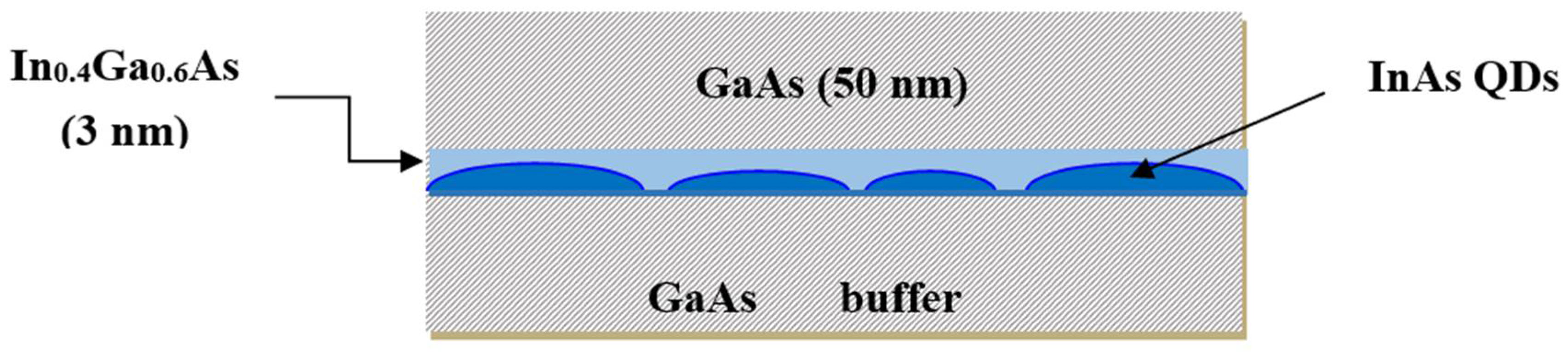
2. Materials and Methods

The studied sample consists of InAs QD formed upon the deposition of 2.4 monolayers InAs followed by a growth interruption of 30 s under As4flux prior to the growth of 3 nm of InGaAs layer with 40% of in composition. This structure has been grown on 0.5 µm GaAs buffer and capped with 50 nm GaAs. All the layers are deposited at 500 °C except the buffer layer, which has been grown at 580 °C. The whole structure, which is schematically presented by Figure 1, has been grown by MBE on SI (001) GaAs substrate. The QD density is estimated by atomic force microscopy to be around 2 × 1010 cm−2.
Sample pieces taken from the fabricated structure have been subjected to thermal treatment in N2 ambient at 650 °C and 750 °C for 50 s. The samples were capped with 200 nm thick SiO2 to protect the surface from excess evaporation and enhance the intermixing process. For PL characterization, the samples were mounted in a closed-cycle Helium cryostat, whichallowed fortuning the temperature from 10 K to 300 K. The 514.5 nm line of an Ar+ laser has been used as an excitation source with an excitation power density of 802 W/cm2. The PL was detected by theInGaAs photodetector using a standard lock-in technique.

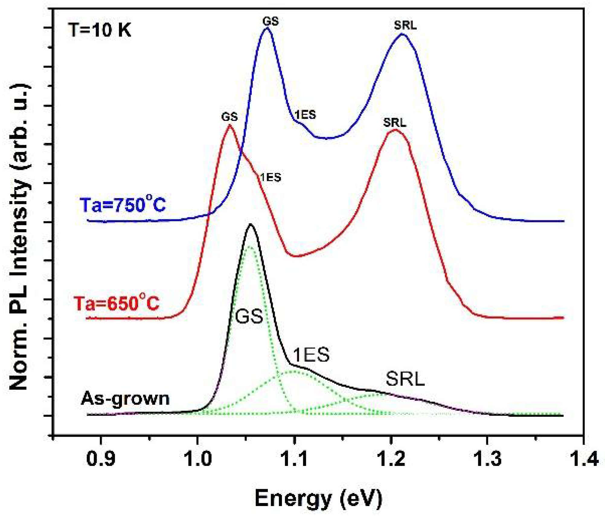
3. Low Temperature PL Properties

As revealed by the Figure 2, the 10 K PL spectra from the as-grown sample shows a dominant emission peak at 1.05 eV with a FWHM around 47 meV, which attributed to the QD ground states transition energy.
A detailed investigation of the higher energy side emission bands have been previously conducted by excitation power dependent PL and PLE, which shows the presence of the excited state emission peak at 1.1 eV as well as a broad (FWHM = 90 meV) emission band around 1.2 eV attributed to the luminescence from the strain-reducing layer [8].
To estimate the buried as-grown QD size, we have numerically solved the single band Schrodinger equation in three dimensions using a finite elements method by taking the strain effects into account for an ellipsoidal-shaped QD. The adequate fitting of the experimental emission energies by changing the QD height and base diameter allows for estimating the buried QD size. The calculation details and fitting procedure can be found in Reference [18]. The best fit has yielded a QD height and base diameter around 2.8 nm and 24 nm, respectively.
After an annealing temperature of 650 °C, the QD emission energy unusually experiences a red shift around 20 meV in addition to a small FWHM decrease by 5 meV. The strain enhanced alloy phase separation during the InGaAs capping layer deposition could alter both the QD size and its environing material’s composition by generating small potential barriers in the vicinity of the QD [19]. During the post-growth annealing process, it is likely that the intermixing tendency to repair the composition fluctuation induces further strain by reducing around the QD and, most likely, a slight size increase [19] leads to the observed PL emission red shift. This interpretation is approved by the strike increase of the InGaAs alloy emission band’s intensity and lowering of its FWHM down to 70 meV.
When the annealing temperature increases to 750 °C, the intermixing seems to overcome the alloy inhomogeneity compensation towards the activation of the intermixing process. This is particularly perceptible through the observed QD PL blue shift up to 1.07 eV with an improved size dispersion (FWHM = 39 meV) in addition to the enhancement of the InGaAs emission peak’s intensity and shrinkage of its linewidth (65 meV).

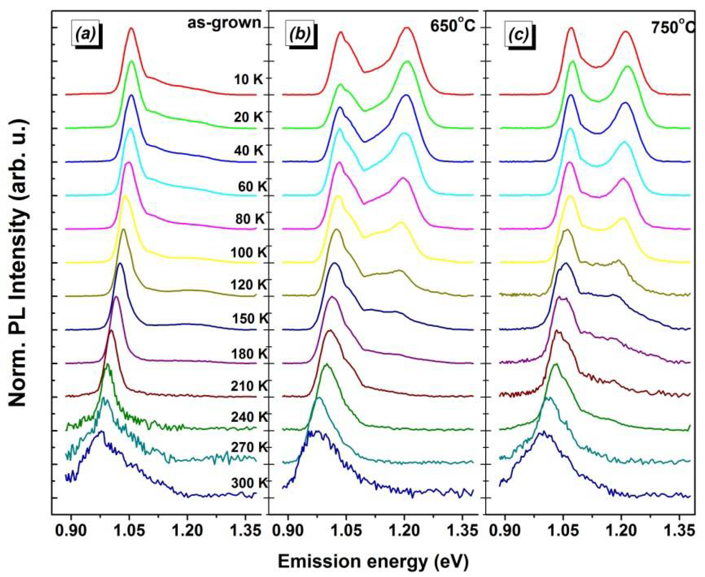
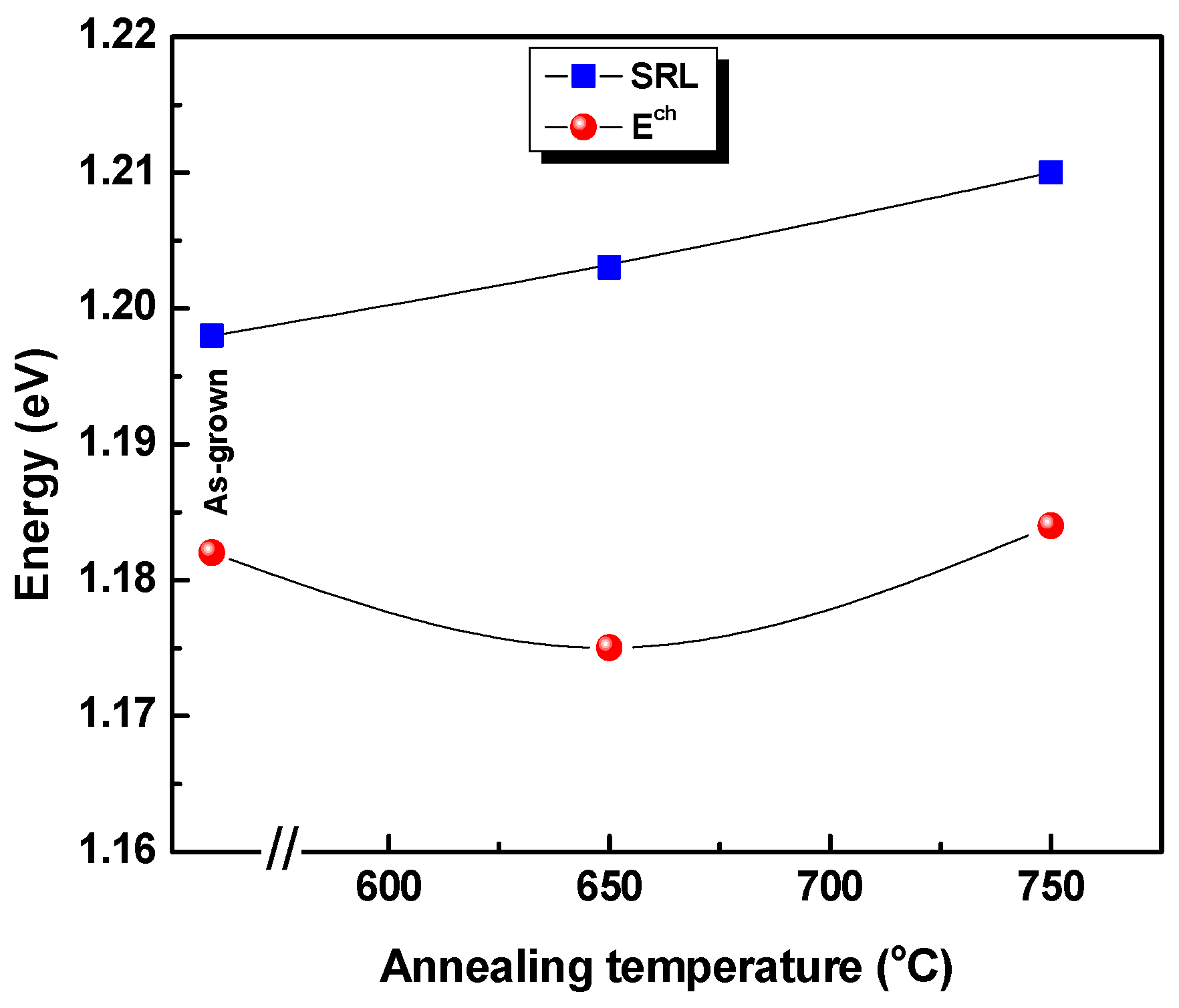
4. Temperature Dependent PL

The evolution of the PL spectra as a function of temperature is shown by Figure 3 for the as-grown and the annealed QD structures. The PL emission band arising from the interband transition in the QW-like SRL quenches for temperature higher than 180 K. This behavior can be interpreted in terms of the lack of confinement in addition to the altered structural properties due to the presence of the QD inside.
Further details on the temperature dependency of the PL properties can be evaluated through the evolution of the QD GS mission energy and PL peak’s FWHM. Accordingly, Figure 4 shows the emission energy from the as-grown QD ground state and those annealed at 650 °C and 750 °C. The emission energy (see Figure 4a) follows the predicted band gap shrinkage by the Varshni law up to 100 K. However, a faster red shift takes place for higher temperature, which leads to a digression from the expected bulk material’s band gap variation.
The sigmoid variation of the emission energy is characteristic of carriers transferring from smaller to larger QD by thermal activation and recapture processes. However, the overall deviation from the bulk InAs material’s band gap shrinkage seems to be reduced by increasing the annealing temperature. This phenomenon can be clearly observed in the PL FWHM dependence on temperature due to the high sensitivity of this parameter to the QD size dispersion. This variation is shown by Figure 4b where the PL FWHM is plotted against temperatures for all samples. Accordingly, the PL linewidth from the as-grown sample first remains constant up to 70 K and then decreases to reach a minimum around 160 K followed by a monotonic increase with an increasing temperature. This atypical variation is found to be progressively flattened out by increasing the annealing temperature.
To gain quantitative information on the carriers’ redistribution processes leading to the observed atypical variation, the LSE model [20] was adopted. It allows for extracting useful parameters such as the carrier transfer channel’s activation energy. The localized states broadening parameter depends on the annealing temperature. It considers that the captured carriers in the QDs states remain localized in the low temperature range. At higher temperature, the carriers get delocalized by thermal activation towards a mediator channel by assisting their recapture and by bigger dots having deeper states.
The LSE model adds a correction term, which contains the broadening parameter and the activation energy towards the carriers’ mediator’s channel to describe the discrepancy with the Varshni relation [21]. The employed InAs constants’ values and details on the model can be found in Reference [9].
As shown by the solid lines in Figure 4, the LSE succeeds in reproducing the unusual temperature-dependent experimental PL emission energy and linewidth. The small discrepancy between the model and the experimental results arising for the PL FWHM is most likely due to extra phenomena, which affects the PL linewidth increase that the model doesn’t take into account such as carriers hopping relaxation.
The expected broadening parameter and carriers activation energies yielding the best fit are listed in Table 1.
The broadening parameter (σ) is found to follow the 10 K-PL linewidth variation. Additionally, σ decreases by raising the annealing temperature describing the improved QD size dispersion (localized states distribution). The carriers get thermally delocalized with increasing temperature from smaller QD and are recaptured by larger ones. The quenching of the luminescence arising from a larger number of small size QD induces shrinkage of the PL linewidth and induces faster emission energies red shift. This process ends at a given temperature where the electron-phonon scattering becomes the PL dominating factor. This induces an increase of the PL linewidth and slows down the emission energy reduction. Obviously, the effect of carriers’ redistribution on both emission energy and PL linewidth is more perceptible for larger QD size distribution [9]. Additionally, the required energy for carrier delocalization from shallower, localized states in smaller QD sizes in a given sample depends on the QD size and composition [22] and could be strongly dependent on the intermixing degree.
At the same time, the extracted activation energy (Ec) depends on the annealing temperature and is found to evolve inversely and proportionally to the variation of the ground state emission energy. Ec reflects the energy barrier height that the carriers need to overcome to reach the transfer channel, which allows for their redistribution by the recapture process. Obviously, deeper localized states require higher activation energy. For this reason, the activation energy is found to increase for an annealing temperature of 650 °C following the observed GS emission red shift and found to decrease for an annealing temperature of 750 °C following the observed GS emission blue shift.
Considering that the delocalization occurs mainly for shallower QD states (smaller sizes), which contributes to the high energy side of the PL emission band, the carriers transfer channel (Ech) can be estimated by adding the activation energy to the smaller size QD emission energy. This is described by the sum of the GS emission peak’s maximum and half of its FWHM, which is shown in the equation below.
E ch = E PL + E c + FWHM 2
Accordingly, we have plotted (see Figure 5) the estimated values for Ech as a function of the annealing temperature together with the emission energy from the SRL.
Ech lays between 20 meV and 35 meV below the maximum of the broad PL emission band from the quantum well like SRL. Furthermore, the SRL emission band is very broad (FWHM ≥ 70 meV), which ensures the overlap with the estimated values of Ech for all the investigated samples. It is, therefore, plausible to consider the SRL continuum states as a possible channel for the transfer of thermally activated carriers from QD with shallow states to larger ones, which leads to the observed behavior as a function of temperature. The minimization of the atypical temperature-dependent emission energy and PL linewidth behavior is likely to be induced by the overall reduction of the QD-size dispersion.

5. Conclusions

The impact of post-growth thermal treatment on InAs QD with high In content InGaAs SRL has been studied by temperature-dependent PL spectroscopy. The atypical PL linewidth and emission energy variation found to occur for the as-grown sample are interpreted in terms of the carriers thermal activation and transfer between QD with different sizes. The uncommon evolutions are found to be progressively evened out by increasing the thermal annealing temperature. The observed behaviors have been discussed in the frame of the LSE model, which allows for identifying the continuum states of the QW-like SRL as a channel for inter-dots carrier transfer.

Author Contributions

B.I. and L.S. designed and performed the experiments. B.I. did the calculation and wrote the paper and N.A.M. analyzed the data. H.M. supervised the work. All the authors have contributed to manuscript revision.

Funding

This research received no external funding.

Acknowledgments

The authors would like to thank the Deanship of Scientific Research at King Saud University for funding this work through the Research Group No: RG-1436-014.

Conflicts of Interest

The authors declare no conflict of interest.

Abbreviations

QDQuantum Dots
QWQuantum Well
MBEMolecular Beam Epitaxy
PLPhotoluminescence
FWHMFull Width at Half Maximum
PLEPhotoluminescence of Excitation
SRLStrain Reducing Layer
LSELocalized States Ensemble

References

  1. Asryan, L.V.; Grundmann, M.; Ledentsov, N.N.; Stier, O.; Suris, R.A.; Bimberg, D. Maximum modal gain of a self-assembled InAs/GaAs quantum-dot laser. J. Appl. Phys. 2001, 90, 1666–1668. [Google Scholar] [CrossRef]
  2. Trotta, R.; Atkinson, P.; Plumhof, J.D.; Zallo, E.; Rezaev, R.O.; Kumar, S.; Baunack, S.; Schröter, J.R.; Rastelli, A.; Schmidt, O.G. Nanomembrane Quantum-Light-Emitting Diodes Integrated onto Piezoelectric Actuators. Adv. Mater. 2012, 24, 2668–2672. [Google Scholar] [CrossRef] [PubMed]
  3. Kita, T.; Suwa, M.; Kaizu, T.; Harada, Y. Polarization-insensitive optical gain characteristics of highly stacked InAs/GaAs quantum dots. J. Appl. Phys. 2014, 115, 233512. [Google Scholar] [CrossRef]
  4. Maimon, S.; Finkman, E.; Bahir, G.; Schacham, S.E.; Garcia, J.M.; Petroff, P.M. Intersublevel transitions in InAs/GaAs quantum dots infrared photodetectors. Appl. Phys. Lett. 1998, 73, 2003–2005. [Google Scholar] [CrossRef] [Green Version]
  5. Bailey, C.G.; Forbes, D.V.; Raffaelle, R.P.; Hubbard, S.M. Near 1 V open circuit voltage InAs/GaAs quantum dot solar cells. Appl. Phys. Lett. 2011, 98, 163105. [Google Scholar] [CrossRef]
  6. Zribi, J.; Ilahi, B.; Paquette, B.; Jaouad, A.; Thériault, O.; Hinzer, K.; Cheriton, R.; Patriarche, G.; Fafard, S.; Aimez, V.; et al. Morris Effect of dot-height truncation on the device performance of multilayer InAs/GaAs quantum dot solar cells. IEEE J. Photovolt. 2016, 6, 584–589. [Google Scholar] [CrossRef]
  7. Weiner, E.C.; Jakomin, R.; Micha, D.N.; Xie, H.; Su, P.Y.; Pinto, L.D.; Pires, M.P.; Ponce, F.A.; Souza, P.L. Effect of capping procedure on quantum dot morphology: Implications on optical properties and efficiency of InAs/GaAs quantum dot solar cells. Sol. Energy Mater. Sol. Cells 2018, 178, 240–248. [Google Scholar] [CrossRef]
  8. Ilahi, B.; Sfaxi, L.; Hassen, F.; Maaref, H.; Salem, B.; Guillot, G.; Jbeli, A.; Marie, X. Optical properties of 1.3 μm room temperature emitting InAs quantum dots covered by In0.4Ga0.6As/GaAs hetero-capping layer. Appl. Phys. A 2005, 81, 813–816. [Google Scholar] [CrossRef]
  9. Ilahi, B.; Nasr, O.; Paquette, B.; Alouane, M.H.H.; Chauvin, N.; Salem, B.; Sfaxi, L.; Bru-Chevalier, C.; Morris, D.; Ares, R.; et al. Thermally activated inter-dots carriers’ transfer in InAs QDs with InGaAs underlying layer: Origin and dependence on the post-growth intermixing. J. Alloys Compd. 2016, 656, 132–137. [Google Scholar] [CrossRef]
  10. Nedzinskas, R.; Čechavičius, B.; Rimkus, A.; Pozingytė, E.; Kavaliauskas, J.; Valušis, G.; Li, L.H.; Linfield, E.H. Temperature-dependent modulated reflectance of InAs/InGaAs/GaAs quantum dots-in-a-well infrared photodetectors. J. Appl. Phys. 2015, 117, 144304. [Google Scholar] [CrossRef]
  11. Nasr, O.; Alouane, M.H.H.; Maaref, H.; Hassen, F.; Sfaxi, L.; Ilahi, B. Comprehensive investigation of optical and electronic properties of tunable InAs QDs optically active at O-band telecommunication window with (In)GaAs surrounding material. J. Lumin. 2014, 148, 243–248. [Google Scholar] [CrossRef]
  12. Lam, P.M.; Wu, J.; Hatch, S.; Kim, D.; Tang, M.; Liu, H.; Wilson, J.; Allison, R. Effect of rapid thermal annealing on InAs/GaAs quantum dot solar cells. IET Optoelectron. 2015, 9, 65–68. [Google Scholar] [CrossRef]
  13. Su, X.B.; Ding, Y.; Ma, B.; Zhang, K.L.; Chen, Z.S.; Li, J.L.; Cui, X.R.; Xu, Y.Q.; Ni, H.Q.; Niu, Z.C. Elimination of Bimodal Size in InAs/GaAs Quantum Dots for Preparation of 1.3-μm Quantum Dot Lasers. Nanoscale Res. Lett. 2018, 13, 59. [Google Scholar] [CrossRef] [PubMed]
  14. Mazur, Y.I.; Dorogan, V.G.; Marega, E., Jr.; Guzun, D.; Ware, M.E.; Zhuchenko, Z.Y.; Tarasov, G.G.; Lienau, C.; Salamo, G.J. Effect of tunneling transfer on thermal redistribution of carriers in hybrid dot-well nanostructures. J. Appl. Phys. 2013, 113, 034309. [Google Scholar] [CrossRef]
  15. Nee, T.E.; Wu, Y.F.; Cheng, C.C.; Shen, H.T. Carrier dynamics study of the temperature and excitation-dependent photoluminescence of InAs/GaAs quantum dots. J. Appl. Phys. 2006, 99, 013506. [Google Scholar] [CrossRef]
  16. Ilahi, B.; Sfaxi, L.; Maaref, H.; Bremond, G.; Guillot, G. Long wavelength vertically stacked InAs/GaAs (001) quantum dots with a bimodal size distribution: Optical properties and electronic coupling. Superlattices Microstruct. 2004, 36, 55–61. [Google Scholar] [CrossRef]
  17. Matutano, M.; Suárez, I.; Canet-Ferrer, J.; Alén, B.; Rivas, D. Size dependent carrier thermal escape and transfer in bimodally distributed self assembledInAs/GaAs quantum dots. J. Appl. Phys. 2012, 111, 123522. [Google Scholar] [CrossRef]
  18. Souaf, M.; Baira, M.; Nasr, O.; Alouane, M.H.H.; Maaref, H.; Sfaxi, L.; Ilahi, B. Investigation of the InAs/GaAs Quantum Dots’ Size: Dependence on the Strain Reducing Layer’s Position. Materials 2015, 8, 4699–4709. [Google Scholar] [CrossRef] [PubMed]
  19. Ilahi, B.; Sfaxi, L.; Maaref, H. Optical investigation of InGaAs-capped InAs quantum dots: Impact of the strain-driven phase separation and dependence upon post-growth thermal treatment. J. Lumin. 2007, 127, 741–746. [Google Scholar] [CrossRef]
  20. Li, Q.; Xu, S.J.; Xie, M.H.; Tong, S.Y. A model for steady-state luminescence of localized-state ensemble. Europhys. Lett. 2005, 71, 994. [Google Scholar] [CrossRef]
  21. Varshni, Y.P. Temperature dependence of the energy gap in semiconductors. Physica 1967, 34, 149. [Google Scholar] [CrossRef]
  22. Talalaev, V.G.; Novikov, B.V.; Smirnov, M.B.; Kachakanov, V.V.; Gobsch, G.; Golhahhn, R.; Winzer, A.; Cirilin, G.E.; Egorov, V.A.; Ustinov, V.M. Photoluminescence of isolated quantum dots in metastable InAs arrays. Nanotechnology 2002, 13, 143. [Google Scholar] [CrossRef]
Figure 1. Schematic presentation of the InAs QDs with In0.4Ga0.6As capping layer.
Crystals 08 00192 g001
Figure 2. 10 K PL spectra taken with an excitation density of 80 W/cm2 from the InAs QDs with In0.4Ga0.6As capping layer: as-grown (black line), annealed at 650 °C (red line), and annealed at 750 °C (blue line). The dotted lines are a Gaussian fit of the as-grown sample’s PL spectra, which shows the emission peaks arising from the ground states (GS), the first excited states (1ES), and the SRL.
Crystals 08 00192 g002
Figure 3. Temperature-dependent PL spectra from the InAs/In0.4Ga0.6As QDs: as-grown (a) annealed at 650 °C (b) and annealed at 750 °C (c).
Crystals 08 00192 g003
Figure 4. PL emission energy (a) and linewidth (b) as a function of temperature from the as-grown sample (red circles) and samples subjected to annealing at 650 °C (blue circles) and 750 °C (green circles). The solid lines indicate the fitting curves by the LSE model and the dotted lines in (a) refer to the band gap shrinkage by using the Varshni law.
Crystals 08 00192 g004
Figure 5. Estimated Ech (filled circles) and the SRL emission energy as a function of the annealing temperature.
Crystals 08 00192 g005
Table 1. Parameters yielding the best fit of the experimental emission energies and PL FWHM by the LSE model.
ParametersAs Grown650 °C750 °C
Ec (meV)11212596
σ (meV)272421

