Article

Atomic Characterization of Byproduct Nanoparticles on Cesium Lead Halide Nanocrystals Using High-Resolution Scanning Transmission Electron Microscopy

National Laboratory of Solid State Microstructures, College of Engineering and Applied Sciences and Collaborative Innovation Center of Advanced Microstructures, Nanjing University, Nanjing 210093, China
*
Author to whom correspondence should be addressed.
Crystals 2018, 8(1), 2; https://doi.org/10.3390/cryst8010002
Submission received: 23 November 2017 / Revised: 20 December 2017 / Accepted: 20 December 2017 / Published: 22 December 2017

Abstract

:
Recent microstructural studies on lead halide perovskite nanocrystals have consistently reported the coexistence of byproduct nanoparticles (NPs). However, the nature of these NPs and their formation mechanism are still a matter of debate. Herein, we have investigated the structure and compositions of the NPs located on colloidal cesium lead bromide nanocrystals (CsPbBr3 NCs), mainly through aberration-corrected transmission electron microscopy and spectroscopy. Our results show that these NPs can be assigned to PbBr2 and CsPb2Br5. The new CsPb2Br5 species are formed by reacting CsPbBr3 NCs with the remaining PbBr2 during the drying process. In addition, observation of the metallic Pb NPs are ascribed to the electron damage effect on CsPbBr3 NCs during transmission electron microscopy imaging.

1. Introduction

Lead halide perovskite (LHP) materials have attracted significant attention in recent years, due to their promising applications in solar cells [1,2,3,4,5], light emitting diodes (LEDs) [6,7,8,9], lasers [10,11,12,13], and photo-detectors [14,15,16,17]. In the family of LHP materials, colloidal all-inorganic cesium lead halide (CsPbX3, X = Cl, Br, and I) perovskite nanocrystals combine both high stability and superior high luminescent efficiency compared to their organic-inorganic counterparts [18,19]. With their colloidal properties, many works have concentrated on applying them to solution-processed devices such as display screens [20], lasers [12] and LEDs [8].
Recent studies have consistently reported the observation of nanoparticles (NPs) with high contrast to LHP nanocrystals (CH3NH3PbBr3 [21] and CsPbBr3 [22,23,24,25,26]) in transmission electron microscopy (TEM) images (i.e., the white dots in Figure 1). However, the structure, chemistry, and forming mechanism of these NPs are still unclear and under debate in these reports. Some reports indicate that these NPs are Pb metal, originating from either the precursor material PbBr2 [26], or the electron damaged CsPbBr3 lattices [23,24,25]. One report suggests that these NPs are PbBr2 [21] and another report claims that these NPs are CsPb2Br5 [22].
Here, we demonstrate that these NPs exist as a mix of PbBr2 and CsPb2Pb5 on the CsPbBr3 nanocrystals (NCs). We propose a formation process of these NPs: (i) Excess reactant of PbBr2 during the synthesis and, subsequently, incomplete purification of the CsPbBr3 products, synergetically lead to excess Pb2+ and Br dissolved in the CsPbBr3 dispersion of nonpolar solvent. After the solvent evaporate from the carbon film, the PbBr2 NPs quickly precipitate on the CsPbBr3 NCs; (ii) The PbBr2 NPs react with part of the CsPbBr3 lattices to form the CsPb2Br5 NPs, still on the CsPbBr3 NCs. Additional observation of the metallic Pb NPs are ascribed to the electron damage effect on CsPbBr3 NCs during TEM imaging.
2. Results and Discussion

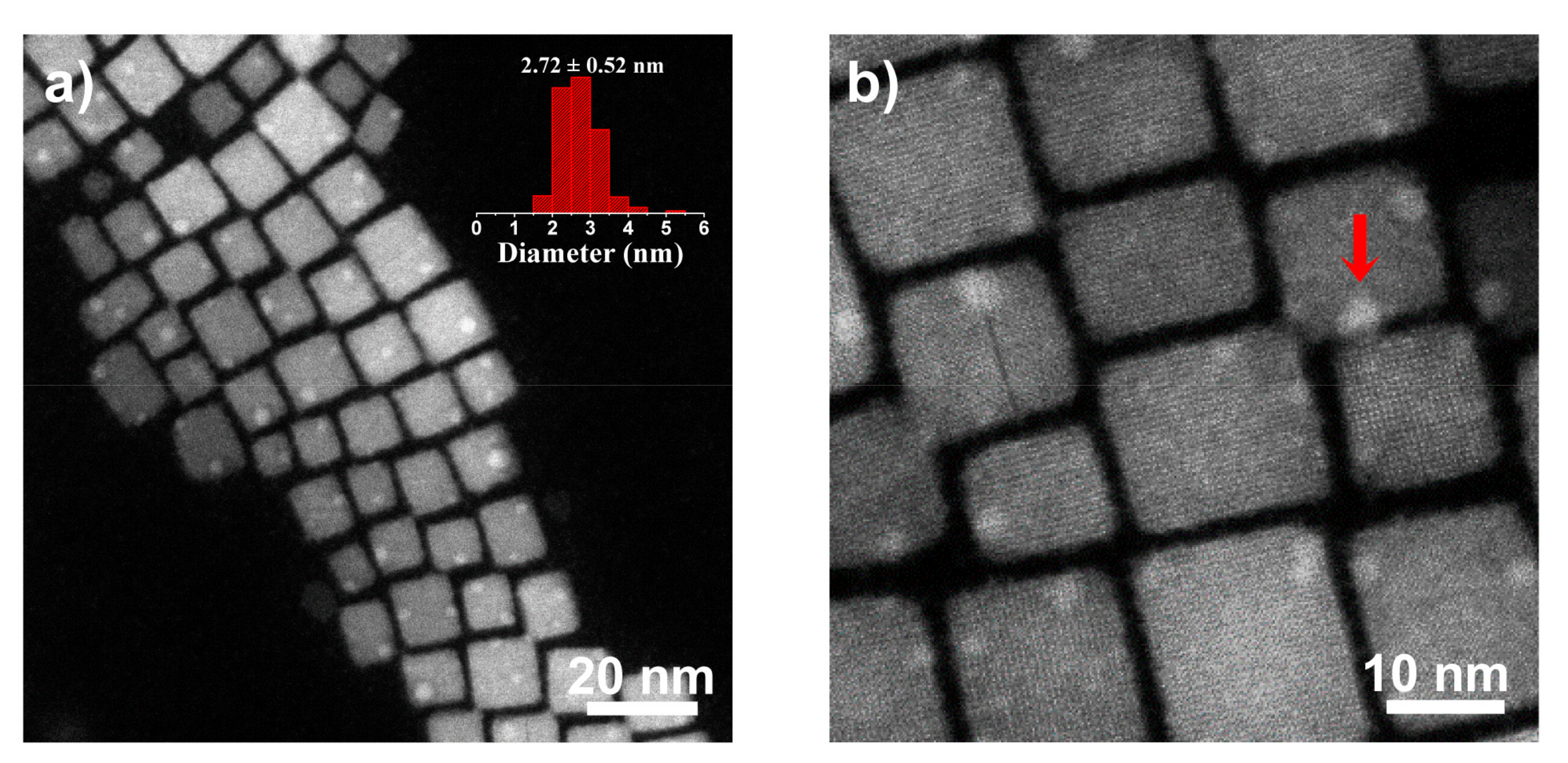
2.1. Morphology, Size, and Position

An overview of the NPs on the CsPbBr3 NCs was first investigated using scanning TEM high-angle annular dark field (STEM-HAADF) images as shown in Figure 1. CsPbBr3 NCs of about 15 nm with cubic and rectangular shapes are demonstrated. The NPs on the CsPbBr3 NCs are of an average size of 2.72 ± 0.52 nm (inset of Figure 1a). These NPs have a tendency to locate near the edge of each CsPbBr3 NC and a NP bridging itself between two CsPbBr3 NCs has been even found (indicated with an arrow in Figure 1b), which suggests that these NPs do not locate inside the CsPbBr3 lattice, but are attached to the surface of CsPbBr3 NCs.

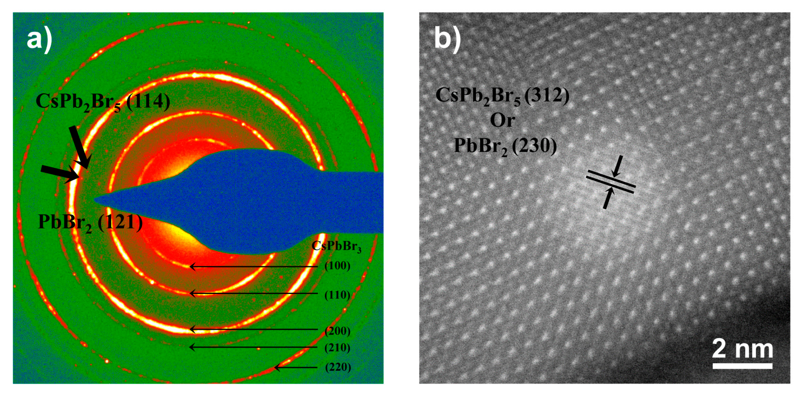
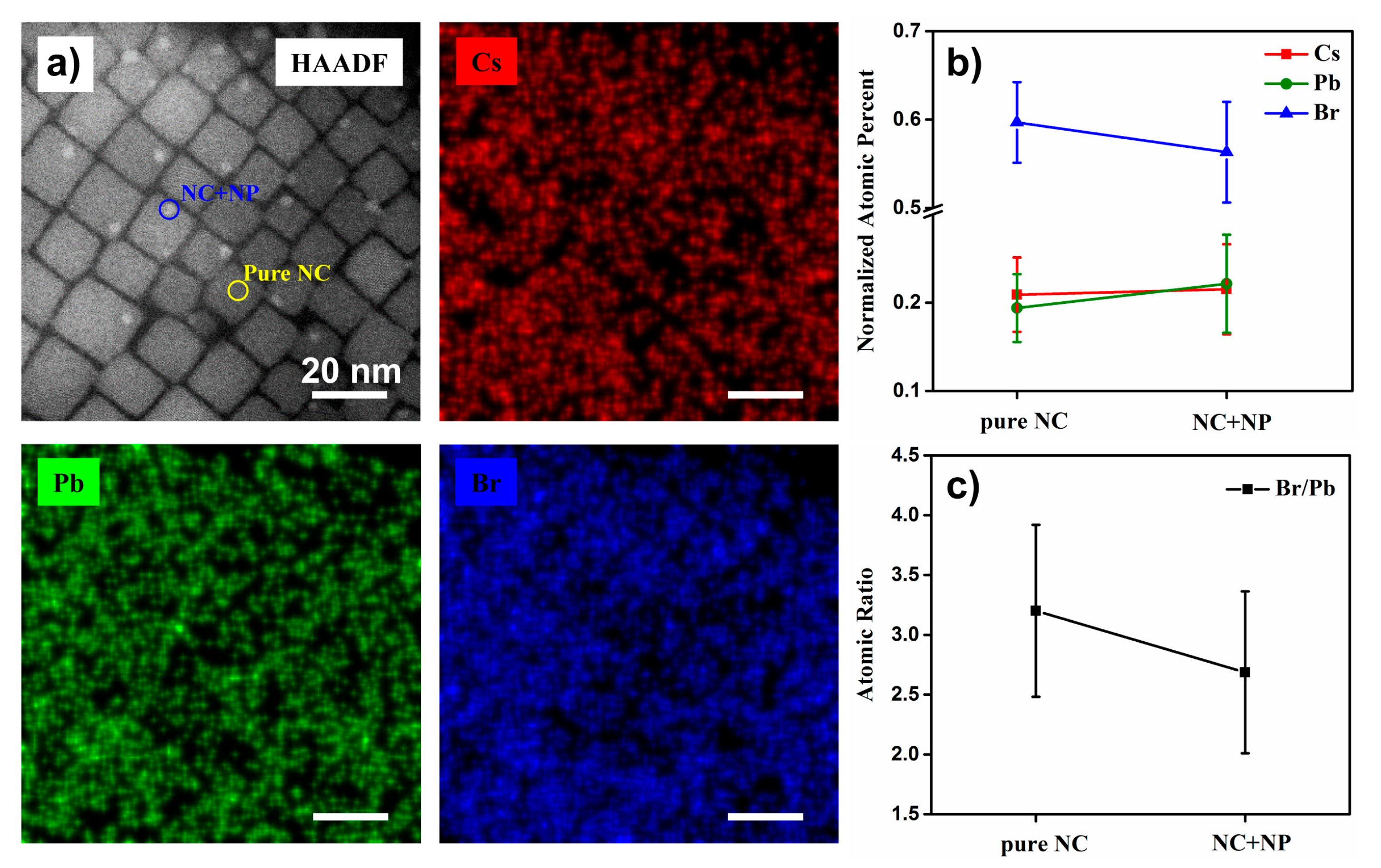
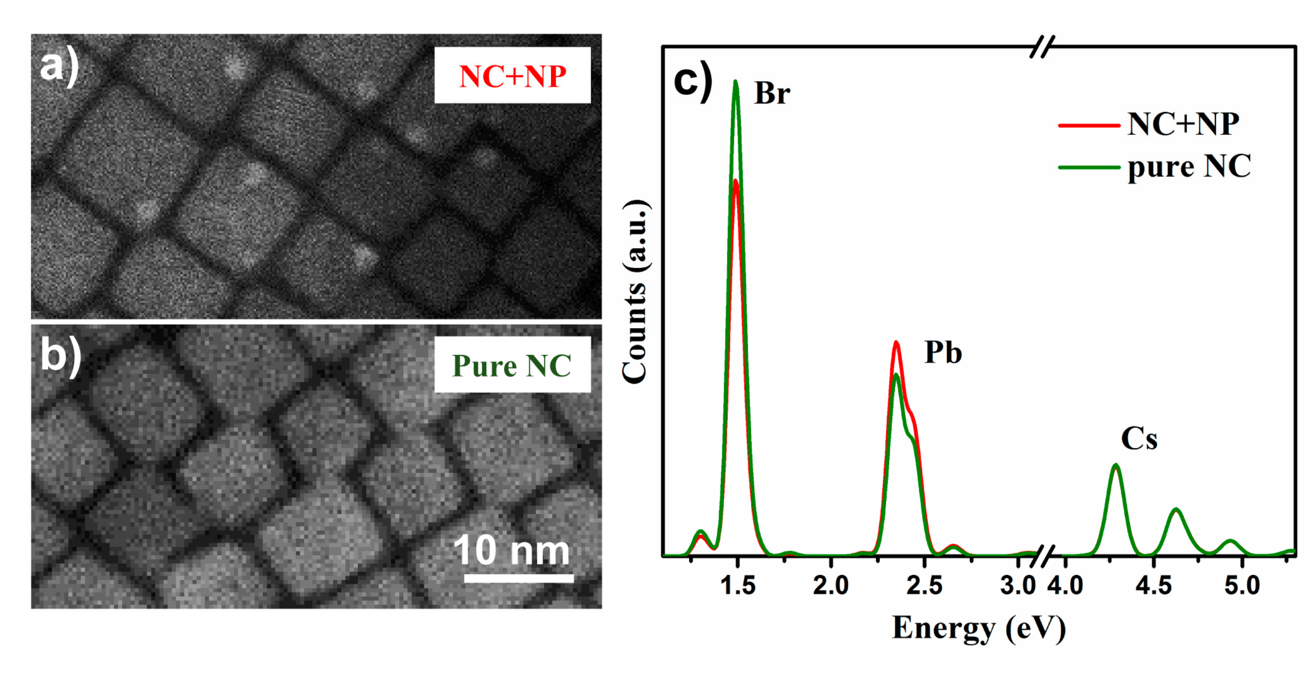
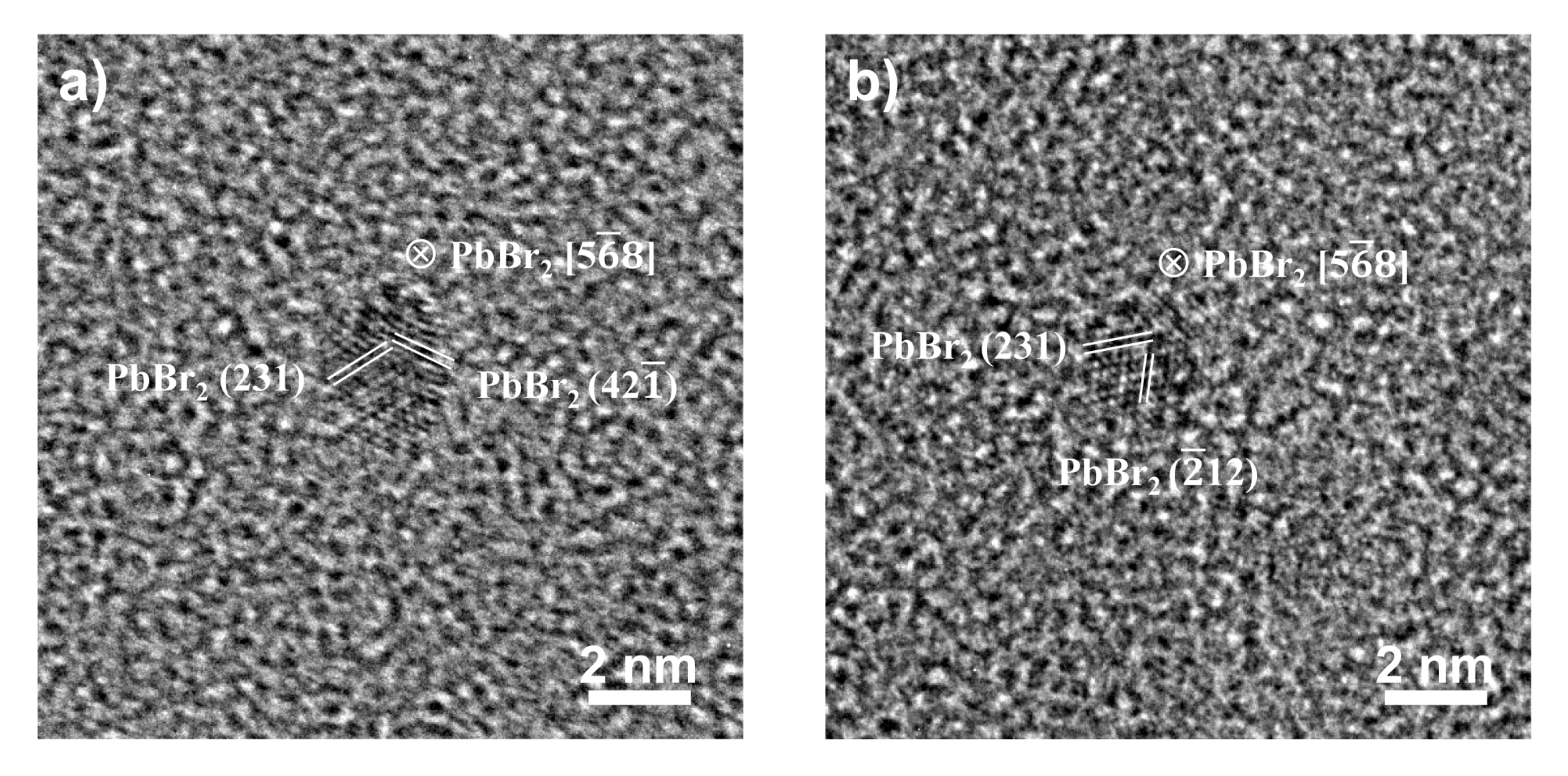
2.2. Structure and Compositions

The structure of these NPs on the CsPbBr3 NCs was first investigated by selected-area electron diffraction (SAED). As shown in Figure 2a, excluding the bright diffractive rings belonging to the CsPbBr3 (100), (110), (200), (210), and (220) planes, additional spots indicated with arrows can be indexed as a PbBr2 (121) plane and a CsPb2Br5 (114) plane. More SAED results are illustrated in Figure S1 to further verify the existence of both PbBr2 NPs and CsPb2Br5 NPs. The identification of PbBr2 and CsPb2Br5 is difficult to directly perform from their weak SAED patterns in the background of those from CsPbBr3 NCs, as most low-index diffraction rings from PbBr2 planes and CsPb2Br5 planes are overlapped with the much brighter ones from CsPbBr3 planes (Table S1). Therefore, while much fewer diffraction spots corresponding to PbBr2 and CsPb2Br5 are found in the SAED patterns compared with the large number of NPs observed in STEM-HAADF images, this is most likely due to the small size and poor crystallinity of the NPs expressing much weaker diffractive signals, largely covered by the signals from carbon films and CsPbBr3 NCs. Later, the existence of the PbBr2 and CsPb2Br5 NPs were further confirmed using high-resolution STEM-HAADF. Figure 2b shows a NP (about 3 nm in diameter) with an interplanar spacing of 2.55 Å, matching well with the CsPb2Br5 (312) plane (a PbBr2 (230) plane is also possible). Note that other possible compounds, including Pb and CsBr, have all been taken into consideration and do not match with the above measurement results. Therefore, the NPs are preliminarily considered as a mix of PbBr2 and CsPb2Br5.
In addition, metallic Pb NPs were also found on CsPbBr3 NCs using high-resolution STEM-HAADF. Figure 3a,b shows the Pb (200) and Pb (020) atomic planes with a lattice spacing of 2.46 Å and an interfacial angle of 90°, oriented along a [001] zone axis. Since previous SAED results (Figure 2a) have implied no existence of metallic Pb, which contradicts the reported argument that metallic Pb NPs exist originally in the CsPbBr3 dispersions [26], the Pb NPs found here at a high magnification (electron dose 1.9 × 10⁵ e2) may, to a large extent, originate from the as-reported electron radiation effect on CsPbBr3 lattice [23,24,25]. From Figure 3b, it is clear to see that the CsPbBr3 lattices under the as-observed Pb NP were modified and damaged. Therefore, we propose that the metallic Pb NPs observed here may not be the extraneous NPs, like the PbBr2 and CsPb2Br5 NPs, but rather a degradation product of CsPbBr3 NCs from the focused electron beam during TEM imaging.
Furthermore, 2D energy dispersive spectroscopy (EDS) elemental mappings of several CsPbBr3 NCs covered with the NPs (Figure 4a) was carried out to study the compositional information of the NPs. Due to the small size of the NPs and corresponding insufficient X-ray counts, the elemental maps (Figure 4a) have not shown strong variations of Cs, Pb, and Br in the position of the NPs. However, when we statistically calculated the atomic percentages of Cs (red), Pb (green), and Br (blue) from regions without the NPs (pure NC, i.e., indicated with a yellow circle in (a)) in comparison to that from regions with the NPs (NC+NP, i.e., indicated with a blue circle in (a)), as plotted in Figure 4b, it is evident to see that the NC+NP regions contain a lower atomic percentage of Br, more of Pb, and a nearly constant percentage of Cs, compared to the pure NC regions. The increment of the Pb percentage in NC+NP regions was most likely caused by the existence of PbBr2 and CsPb2Br5 NPs. However, a question may arise that, if the NPs consisted of PbBr2 and CsPb2Br5, the Br percentage should, in theory, increase, which is unexpectedly inconsistent with the experimental data (blue curve) in Figure 4b.
In order to understand this discrepancy, we further directly compare the integrated EDS spectra of Cs, Pb, and Br taken from both NC+NP (a) and pure NC (b) regions, as shown in Figure 5. The two spectra were normalized with the peak of Cs as the only reactant of PbBr2 was in excess during the synthesis. Regarding the signal of Br, it unexpectedly decreases for the NC+NP region compared to the pure NC region. In theory, the signal of Br should increase for the NC+NP region, if the additional NPs consisted of PbBr2 and CsPb2Br5. However, by considering the inevitable electron-induced Br loss during EDS measurements [25], there is a high possibility that the existence of these NPs may lead to the structural instability of CsPbBr3. As a result, the NC+NP region might have undergone an even more severe electron damage effect compared to the pure NC region, so that the electron-induced Br loss may surpass the theoretical Br increase coming from the extra existence of PbBr2 and CsPb2Br5 NPs, causing the total Br intensity to decrease, as shown in Figure 5b and the Br percentage to unexpectedly decrease in Figure 4b. It can be concluded that the increase of the Pb percentage found in Figure 4b is not only due to the excess of PbBr2 and CsPb2Br5 NPs, but also the Br loss induced by the strong electron damage effect in the NC+NP regions. It can also be understood that the atomic Br/Pb ratio (Figure 4c) being lower for the NC+NP regions, may be due to the interplay of the existence of PbBr2 and CsPb2Br5 NPs whose Br/Pb ratio are lower than the stoichiometric one (3:1), and the Br loss induced by the strong electron damage effect in the NC+NP regions during EDS measurements. In addition, the increase of Pb intensity in the NC+NP region in Figure 5b further confirms that an excess Pb content exists in the NC+NP region, most likely in the forms of PbBr2 and CsPb2Br5 NPs in addition to CsPbBr3.

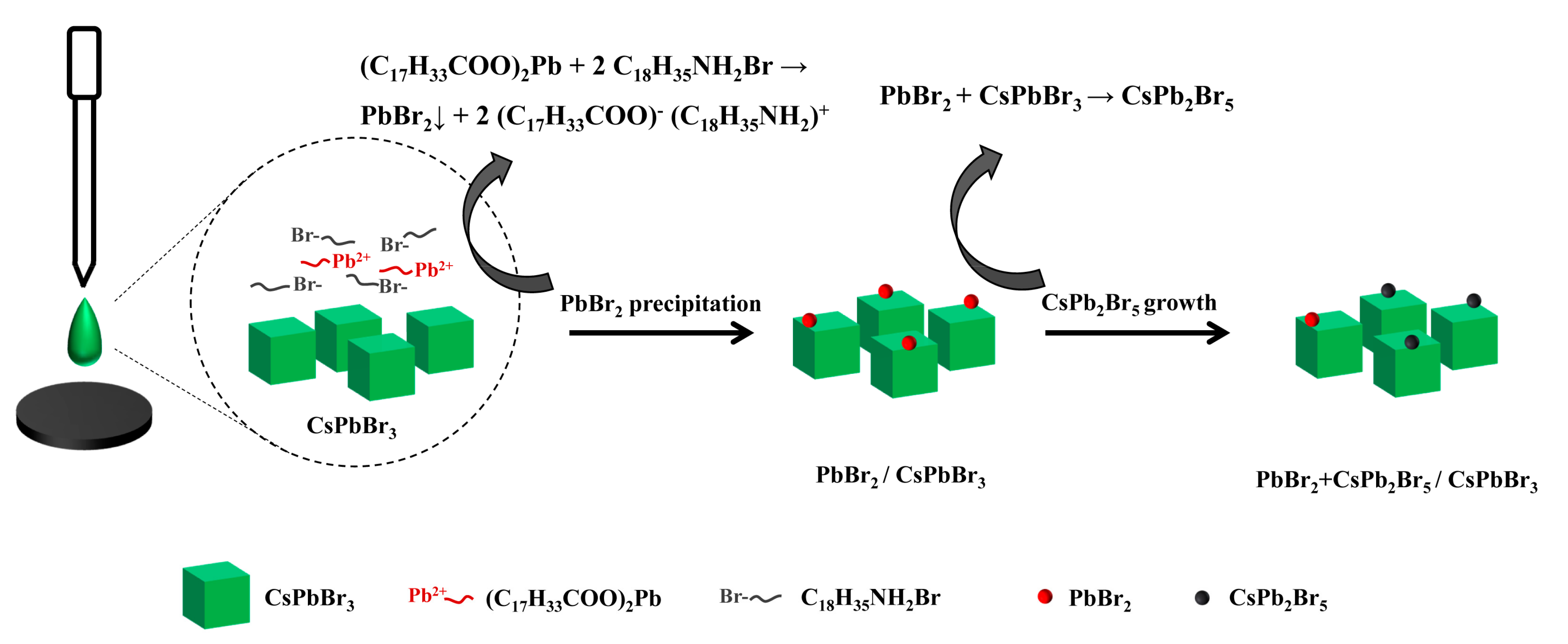
2.3. Formation Mechanism

Here we suppose that the presence of PbBr2 NPs can be ascribed to the excess PbBr2 in the CsPbBr3 dispersions. In our synthesis, molar ratio of reactant Cs:Pb:Br is controlled at about 1:3.3:6.6, which is similar to the most reported hot-injection procedures. Obviously, according to the stoichiometry ratio of CsPbBr3 NCs, Cs species work as a limiting agent, and PbBr2 is highly excessive in this reaction. In addition, incomplete purification of the CsPbBr3 products during the following centrifugation step enables excess PbBr2 to be left in the final CsPbBr3 dispersions [27], existing as ion-complexes with oleic acid or oleylamine. When the drop of CsPbBr3 dispersions on the ultrathin carbon film evaporates, the CsPbBr3 NCs are spread out on the carbon film while the PbBr2 NPs would precipitate on the carbon film or the upper surface of the NCs (Figure 6). This is consistent with the previous observation that the NPs are preferentially located at the corners and edges of the surface of CsPbBr3 NCs. The chemical equilibrium reaction involved is as follows:
( C 17 H 33 COO ) 2 Pb   +   2 C 18 H 35 NH 2 Br     PbBr 2 +   2 ( C 17 H 33 COO ) ( C 18 H 35 NH 2 ) +
As the reaction shows, PbBr2 would precipitate out, while oleate and oleylammonium form ion pairs. We note that if the above reaction was not complete, lead oleate and oleylammonium bromide may also precipitate out as separate species in the NPs. However, as it is difficult to directly characterize the structures of these organic non-crystalline materials through TEM imaging, the existence of lead oleate and oleylammonium bromide are not discussed here and are subject to future investigation.
Few reports have referred to the source of CsPb2Br5. One report demonstrated the existence of 10% CsPb2Br5 in the CsPbBr3 solutions at room temperature [28]. Another report suggested that the excess PbBr2 facilitates a structural transformation of small CsPbBr3 nanocrystals in the precursor into CsPb2Br5 at a low temperature [22]. A recent report verified CsPbBr3 nanocrystals can transfer to CsPb2Br5 nanosheets as the reaction time prolongs, clearly indicating this conversion (from CsPbBr3 to CsPb2Br5) is thermodynamically favorable [29]. Therefore, we propose that the generation of CsPb2Br5 can be ascribed to the following process:
PbBr 2   +   CsPbBr 3     CsPb 2 Br 5
The precipitated PbBr2 NPs touch the CsPbBr3 NC surface and tend to facilitate the generation of CsPb2Br5 NPs, as illustrated in Figure 6.
To confirm the contribution of excess PbBr2 to the existence of the NPs, the remaining amount of PbBr2 in the CsPbBr3 dispersions were changed. Since directly changing the reactant amount may destroy the synthesis, we changed the purification times of the as-synthesized CsPbBr3 products instead. Therefore, a comparison was made through TEM characterization between the following two samples: CsPbBr3 NCs washed one time and CsPbBr3 NCs washed three times. For the one-time wash sample, it is clear to see in Figure 7 that the NPs are evenly distributed both on the CsPbBr3 NCs (a) and the carbon film (b), whereas for the sample washed three times with acetone, none of the NPs were found, neither on CsPbBr3 NCs (c) or the carbon film (d). Moreover, the microstructure of the NPs on the carbon film was further confirmed by high-resolution TEM imaging and EDS elemental mapping. Figure 8a,b shows the high-resolution TEM images of two NPs on the carbon film. As shown in Figure 8a, the interplanar spacings of the NPs match well with the PbBr2 (231) and (42 1 ¯ ) planes with an interfacial angle of 56°, oriented along a [5 6 ¯ 8] axis. Additionally, in Figure 8b, the interplanar spacing of the NPs match well with the PbBr2 (231) and ( 2 ¯ 12) planes with an interfacial angle of 74°, oriented along a [5 6 ¯ 8] axis. Additionally, EDS measurements reveal that these NPs on the carbon film contain both Br and Pb, but lack Cs (See Figure S2 and Table S2). As a result, the unwashed NPs on the carbon film are verified to be PbBr2. Therefore, it is confirmed that the excess reactant of PbBr2 and incomplete purification contribute to the existence of the PbBr2 NPs on both CsPbBr3 NCs and carbon films.
As for the metallic Pb NPs, it was reported that the Pb NPs were formed in the PbBr2 solution prior to injection of Cs salt [23], while another report investigated the effects of high energy electron radiation contributing to Br atoms desorption and Pb atoms crystallization [25]. Since previous SAEDs have indicated no Pb metals to exist, we assume that the original CsPbBr3 dispersions have contained no Pb metals. Therefore, the observed Pb NPs by high-resolution HAADF-STEM might result from the electron damage effect on CsPbBr3 NCs. Electron radiation (300 keV) induces desorption of Br atoms from the surface of the NCs and reduces Pb2+ cations to metallic Pb0 atoms. Pb0 atoms diffuse and aggregate into Pb NPs, oriented epitaxially on the CsPbBr3 lattice.

3. Materials and Methods

3.1. Materials

Oleic acid (OA 90%), octadecene (ODE 90%), oleylamine (OAM 80–90%), cyclohexane, acetone, cesium carbonate (Cs2CO3 99.9%), and lead bromide (PbBr2 99.999%) were purchased from Aladdin (Shanghai, China). All chemicals were used as received without any further purification.

3.2. Synthesis of CsPbBr3 Perovskite NCs

The CsPbBr3 perovskite NCs adopted here were fabricated following a hot injection method [30]. For the synthesis of the CsPbBr3, 0.1 g of PbBr2 was added into a mixture of 7.5 mL ODE, 1.5 mL OAM, and 0.75 mL OA, and then heated to 120 °C for 30 min under vacuum. The temperature was then raised to 150 °C, followed by the rapid injection of 0.7 mL of Cs-oleate solution (0.407 g Cs2CO3 dissolved within 20 mL ODE and 1.5 mL OA). After several seconds, the solution was rapidly cooled by the water bath. The products were then washed via centrifugation with cyclohexane/acetone for one or three times. Finally the products were dispersed in cyclohexane forming long-term colloidally-stable dispersions.

3.3. Characterization of the NPs on the CsPbBr3 NCs

TEM images, selected-area electron diffraction (SAED) patterns and scanning TEM high angle annular dark field (STEM-HAADF) images were acquired using a FEI Tecnai G2 F20 S-TWIN microscope, operated at an accelerating voltage of 200 kV. High-resolution TEM images, high-resolution STEM-HAADF images [31], and energy-dispersive spectroscopy (EDS) elemental mappings were acquired using a FEI Titan3 G2 60-300 microscope, operated at an accelerating voltage of 300 kV, equipped with double aberration correctors [32] and Super-X EDS detectors [33]. The image pixel size in the high-resolution TEM and high-resolution STEM-HAADF images was calibrated using the ratio of the CsPbBr3 lattice constant listed in the PDF card (CsPbBr3, cubic phase, PDF#75-0412) to the corresponding interplanar spacing pixels of the CsPbBr3 NC measured in the image at the same magnification.

4. Conclusions

The TEM experiments presented here demonstrate that the byproduct NPs on CsPbBr3 NCs is a mix of PbBr2 and CsPb2Br5. We propose here that the excess reactant of PbBr2 during the synthesis and, subsequently, the incomplete purification of the CsPbBr3 products, synergetically led to the final excess precipitation of the PbBr2 NPs on CsPbBr3 NCs after solvent evaporation. The subsequent reaction between the PbBr2 NPs and the CsPbBr3 surface induce the formation of the CsPb2Br5 NPs. Moreover, the existence of these NPs may add to the structural instability of CsPbBr3, so methods to remove these NPs are of great importance for maintaining their superior optical properties. Here, we propose that these byproduct NPs can be fully removed via washing CsPbBr3 NCs three times with acetone. In addition, the metallic Pb NPs, which were not found in the original CsPbBr3 dispersions, could be attributed to the electron damage of CsPbBr3 NCs during TEM imaging. The above formation mechanism of the NPs on CsPbBr3 NCs may also apply to other CsPbX3 and hybrid lead halide perovskite nanocrystals.

Supplementary Materials

The following are available online at www.mdpi.com/2073-4352/8/1/2/s1; Figure S1: SAED patterns from two 0.48 μm2 areas of the NPs on the CsPbBr3 NCs; Figure S2: An integrated EDS spectrum acquired from a region with the NPs on a carbon film; Table S1: Interplanar spacings of CsPbBr3, PbBr2, and CsPb2Br5, respectively; Table S2: Atomic percentages of Cs, Pb, and Br for a region with the NPs on a carbon film.

Acknowledgments

This work was supported by the National Basic Research Program of China (grant no. 2015CB654901); the National Natural Science Foundation of China (11474147); the Natural Science Foundation of Jiangsu Province (grant no. BK20151383); the International Science and Technology Cooperation Program of China (2014DFE00200); and the Fundamental Research Funds for the Central Universities (no. 021314380077).

Author Contributions

Mian Zhang designed the experiments. Hongbo Li and Qiang Jing contributed sample materials. Mian Zhang performed the experiments and analyzed the dataset. Zhenda Lu and Peng Wang designed, supervised the project, and interpreted data.

Conflicts of Interest

The authors declare no conflict of interest.

References

  1. Kojima, A.; Teshima, K.; Shirai, Y.; Miyasaka, T. Organometal halide perovskites as visible-light sensitizers for photovoltaic cells. J. Am. Chem. Soc. 2009, 131, 6050–6051. [Google Scholar] [CrossRef] [PubMed]
  2. Lee, M.M.; Teuscher, J.; Miyasaka, T.; Murakami, T.N.; Snaith, H.J. Efficient hybrid solar cells based on meso-superstructured organometal halide perovskites. Science 2012, 338, 643–647. [Google Scholar] [CrossRef] [PubMed]
  3. Liu, D.; Kelly, T.L. Perovskite solar cells with a planar heterojunction structure prepared using room-temperature solution processing techniques. Nat. Photonics 2014, 8, 133–138. [Google Scholar] [CrossRef]
  4. Liu, M.; Johnston, M.B.; Snaith, H.J. Efficient planar heterojunction perovskite solar cells by vapour deposition. Nature 2013, 501, 395–398. [Google Scholar] [CrossRef] [PubMed]
  5. Yang, W.S.; Noh, J.H.; Jeon, N.J.; Kim, Y.C.; Ryu, S.; Seo, J.; Seok, S.I. High-performance photovoltaic perovskite layers fabricated through intramolecular exchange. Science 2015, 348, 1234–1237. [Google Scholar] [CrossRef] [PubMed]
  6. Cho, H.; Jeong, S.-H.; Park, M.-H.; Kim, Y.-H.; Wolf, C.; Lee, C.-L.; Heo, J.H.; Sadhanala, A.; Myoung, N.; Yoo, S. Overcoming the electroluminescence efficiency limitations of perovskite light-emitting diodes. Science 2015, 350, 1222–1225. [Google Scholar] [CrossRef] [PubMed]
  7. Kim, Y.H.; Cho, H.; Heo, J.H.; Kim, T.S.; Myoung, N.; Lee, C.L.; Im, S.H.; Lee, T.W. Multicolored Organic/Inorganic Hybrid Perovskite Light-Emitting Diodes. Adv. Mater. 2015, 27, 1248–1254. [Google Scholar] [CrossRef] [PubMed]
  8. Song, J.; Li, J.; Li, X.; Xu, L.; Dong, Y.; Zeng, H. Quantum Dot Light-Emitting Diodes Based on Inorganic Perovskite Cesium Lead Halides (CsPbX3). Adv. Mater. 2015, 27, 7162–7167. [Google Scholar] [CrossRef] [PubMed]
  9. Tan, Z.-K.; Moghaddam, R.S.; Lai, M.L.; Docampo, P.; Higler, R.; Deschler, F.; Price, M.; Sadhanala, A.; Pazos, L.M.; Credgington, D. Bright light-emitting diodes based on organometal halide perovskite. Nat. Nanotechnol. 2014, 9, 687–692. [Google Scholar] [CrossRef] [PubMed]
  10. D’Innocenzo, V.; Srimath Kandada, A.R.; De Bastiani, M.; Gandini, M.; Petrozza, A. Tuning the light emission properties by band gap engineering in hybrid lead halide perovskite. J. Am. Chem. Soc. 2014, 136, 17730–17733. [Google Scholar] [CrossRef] [PubMed]
  11. Deschler, F.; Price, M.; Pathak, S.; Klintberg, L.E.; Jarausch, D.-D.; Higler, R.; Huttner, S.; Leijtens, T.; Stranks, S.D.; Snaith, H.J. High photoluminescence efficiency and optically pumped lasing in solution-processed mixed halide perovskite semiconductors. J. Phys. Chem. Lett. 2014, 5, 1421–1426. [Google Scholar] [CrossRef] [PubMed]
  12. Yakunin, S.; Protesescu, L.; Krieg, F.; Bodnarchuk, M.I.; Nedelcu, G.; Humer, M.; De Luca, G.; Fiebig, M.; Heiss, W.; Kovalenko, M.V. Low-threshold amplified spontaneous emission and lasing from colloidal nanocrystals of caesium lead halide perovskites. Nat. Commun. 2015, 6, 8056. [Google Scholar] [CrossRef] [PubMed]
  13. Zhu, H.; Fu, Y.; Meng, F.; Wu, X.; Gong, Z.; Ding, Q.; Gustafsson, M.V.; Trinh, M.T.; Jin, S.; Zhu, X. Lead halide perovskite nanowire lasers with low lasing thresholds and high quality factors. Nat. Mater. 2015, 14, 636–642. [Google Scholar] [CrossRef] [PubMed]
  14. Fang, Y.; Dong, Q.; Shao, Y.; Yuan, Y.; Huang, J. Highly narrowband perovskite single-crystal photodetectors enabled by surface-charge recombination. Nat. Photonics 2015, 9, 675–686. [Google Scholar] [CrossRef]
  15. Hu, X.; Zhang, X.; Liang, L.; Bao, J.; Li, S.; Yang, W.; Xie, Y. High-performance flexible broadband photodetector based on organolead halide perovskite. Adv. Funct. Mater. 2014, 24, 7373–7380. [Google Scholar] [CrossRef]
  16. Lee, Y.; Kwon, J.; Hwang, E.; Ra, C.H.; Yoo, W.J.; Ahn, J.H.; Park, J.H.; Cho, J.H. High-performance perovskite–graphene hybrid photodetector. Adv. Mater. 2015, 27, 41–46. [Google Scholar] [CrossRef] [PubMed]
  17. Yakunin, S.; Sytnyk, M.; Kriegner, D.; Shrestha, S.; Richter, M.; Matt, G.J.; Azimi, H.; Brabec, C.J.; Stangl, J.; Kovalenko, M.V. Detection of X-ray photons by solution-processed lead halide perovskites. Nat. Photonics 2015, 9, 444–449. [Google Scholar] [CrossRef] [PubMed]
  18. Protesescu, L.; Yakunin, S.; Bodnarchuk, M.I.; Krieg, F.; Caputo, R.; Hendon, C.H.; Yang, R.X.; Walsh, A.; Kovalenko, M.V. Nanocrystals of cesium lead halide perovskites (CsPbX3, X = Cl, Br, and I): Novel optoelectronic materials showing bright emission with wide color gamut. Nano Lett. 2015, 15, 3692–3696. [Google Scholar] [CrossRef] [PubMed] [Green Version]
  19. Wang, Y.; Li, X.; Song, J.; Xiao, L.; Zeng, H.; Sun, H. All-inorganic colloidal perovskite quantum dots: A new class of lasing materials with favorable characteristics. Adv. Mater. 2015, 27, 7101–7108. [Google Scholar] [CrossRef] [PubMed]
  20. Yoon, H.C.; Kang, H.; Lee, S.; Oh, J.H.; Yang, H.; Do, Y.R. Study of perovskite QD down-converted LEDs and six-color white LEDs for future displays with excellent color performance. ACS Appl. Mater. Interfaces 2016, 8, 18189–18200. [Google Scholar] [CrossRef] [PubMed]
  21. Sichert, J.A.; Tong, Y.; Mutz, N.; Vollmer, M.; Fischer, S.; Milowska, K.Z.; García Cortadella, R.; Nickel, B.; Cardenas-Daw, C.; Stolarczyk, J.K. Quantum size effect in organometal halide perovskite nanoplatelets. Nano Lett. 2015, 15, 6521–6527. [Google Scholar] [CrossRef] [PubMed]
  22. Zhang, X.; Xu, B.; Zhang, J.; Gao, Y.; Zheng, Y.; Wang, K.; Sun, X.W. All-inorganic perovskite nanocrystals for high-efficiency light emitting diodes: Dual-phase cspbbr3-cspb2br5 composites. Adv. Funct. Mater. 2016, 26, 4595–4600. [Google Scholar] [CrossRef]
  23. Van der, S.W.; Geuchies, J.J.; Altantzis, T.; Kh, V.D.B.; Meeldijk, J.D.; Van, A.S.; Bals, S.; Vanmaekelbergh, D.; De, M.D.C. Highly emissive divalent-ion-doped colloidal cspb1-xmxbr3 perovskite nanocrystals through cation exchange. J. Am. Chem. Soc. 2017, 139, 4087–4097. [Google Scholar] [CrossRef] [PubMed]
  24. Tong, Y.; Bladt, E.; Aygüler, M.F.; Manzi, A.; Milowska, K.Z.; Hintermayr, V.A.; Docampo, P.; Bals, S.; Urban, A.S.; Polavarapu, L. Highly luminescent cesium lead halide perovskite nanocrystals with tunable composition and thickness by ultrasonication. Angew. Chem. 2016, 55, 13887–13892. [Google Scholar] [CrossRef] [PubMed]
  25. Dang, Z.; Shamsi, J.; Palazon, F.; Imran, M.; Akkerman, Q.A.; Park, S.; Bertoni, G.; Prato, M.; Brescia, R.; Manna, L. In Situ Transmission Electron Microscopy Study of electron beam-induced transformations in colloidal cesiumlead halide perovskite nanocrystals. Acs Nano 2017, 11, 2124–2132. [Google Scholar] [CrossRef] [PubMed]
  26. Udayabhaskararao, T.; Kazes, M.; Houben, L.; Lin, H.; Oron, D. Nucleation, growth, and structural transformations of perovskite nanocrystals. Chem. Mater. 2017, 29, 1302–1308. [Google Scholar] [CrossRef]
  27. Gonzalez-Carrero, S.; Galian, R.E.; Pérez-Prieto, J. Maximizing the emissive properties of CH3NH3PbBr3 perovskite nanoparticles. J. Mater. Chem. A 2015, 3, 9187–9193. [Google Scholar] [CrossRef]
  28. Rodová, M.; Brožek, J.; Knížek, K.; Nitsch, K. Phase transitions in ternary caesium lead bromide. J. Therm. Anal. Calorim. 2003, 71, 667–673. [Google Scholar] [CrossRef]
  29. Li, G.; Wang, H.; Zhu, Z.; Chang, Y.; Zhang, T.; Song, Z.; Jiang, Y. Shape and phase evolution from CsPbBr3 perovskite nanocubes to tetragonal CsPb2Br5 nanosheets with an indirect bandgap. Chem. Commun. 2016, 52, 11296–11299. [Google Scholar] [CrossRef] [PubMed]
  30. Talapin, D.V.; Lee, J.-S.; Kovalenko, M.V.; Shevchenko, E.V. Prospects of colloidal nanocrystals for electronic and optoelectronic applications. Chem. Rev. 2009, 110, 389–458. [Google Scholar] [CrossRef] [PubMed]
  31. Muller, D.A. Structure and bonding at the atomic scale by scanning transmission electron microscopy. Nat. Mater. 2009, 8, 263–270. [Google Scholar] [CrossRef] [PubMed]
  32. Hutchison, J.L.; Titchmarsh, J.M.; Cockayne, D.J.; Doole, R.C.; Hetherington, C.J.; Kirkland, A.I.; Sawada, H. A versatile double aberration-corrected, energy filtered HREM/STEM for materials science. Ultramicroscopy 2005, 103, 7–15. [Google Scholar] [CrossRef] [PubMed]
  33. Allen, L.J.; D’Alfonso, A.J.; Freitag, B.; Klenov, D.O. Chemical mapping at atomic resolution using energy-dispersive X-ray spectroscopy. MRS Bull. 2012, 37, 47–52. [Google Scholar] [CrossRef]
Figure 1. Overview STEM-HAADF images of the NPs on the CsPbBr3 NCs at different magnifications. The inset of (a) shows the size distribution of over 300 NPs. The red arrow in (b) indicates a NP bridging itself between two CsPbBr3 NCs.
Crystals 08 00002 g001
Figure 2. (a) SAED pattern of the NPs on the CsPbBr3 NCs. Arrowed spots can be identified as PbBr2 NPs and CsPb2Br5 NPs, excluding the main diffraction rings belonging to various CsPbBr3 planes. (b) High-resolution STEM-HAADF image of a CsPb2Br5 NP (a PbBr2 NP is also possible) formed on the CsPbBr3 NC (CsPbBr3, cubic phase, PDF#75-0412; PbBr2, orthorhombic phase, PDF#31-0679; CsPb2Br5, tetragonal phase, PDF#25-0211).
Crystals 08 00002 g002
Figure 3. High-resolution STEM-HAADF images of the Pb NPs on the CsPbBr3 NCs with [001] orientation (Pb, cubic phase, PDF#87-0663).
Crystals 08 00002 g003
Figure 4. (a) STEM-EDS raw counts mappings of CsPbBr3 NCs with the NPs. No strong variations of Cs, Pb, or Br are found in the position of the NPs. None of the auto-filter processing is applied here. (b) A plot of the calculated atomic percentages for Cs, Pb, and Br versus different regions (pure NC regions and NC+NP regions). We took an average of 10 quantified elemental atomic percentage results subtracted from 10 pure NC regions (i.e., indicated by a yellow circle in (a)). The error bar is the standard deviation. Similar calculations were applied to the NC+NP regions (i.e., indicated by a blue circle in (a)). (c) A plot of calculated atomic ratio of Br/Pb versus different regions (pure NC regions and NC+NP regions).
Crystals 08 00002 g004
Figure 5. HAADF images of the NC+NP (a) and pure NC (b) regions. (c) Integrated EDS spectra acquired from NC+NP () and pure NC (―) regions as shown in (a) and (b), respectively.
Crystals 08 00002 g005
Figure 6. Schematic of the formation mechanism of the PbBr2 NPs and the CsPb2Br5 NPs on CsPbBr3 NCs.
Crystals 08 00002 g006
Figure 7. HAADF-STEM images of the distribution of the NPs on both CsPbBr3 NCs and carbon films for the sample washed one time (a,b) and the sample washed three times (c,d), respectively.
Crystals 08 00002 g007
Figure 8. High-resolution TEM images of the PbBr2 NPs found on carbon films along a [5 6 ¯ 8] axis.
Crystals 08 00002 g008

