1. Introduction
Since Novoselov
et al. [
1] and Zhang
et al. [
2] experimentally demonstrated that graphene is a zero-gap system with massless Dirac particles, such systems have fascinated physicists as a source of exotic systems and/or new physics. At the same time, the quasi-two-dimensional (2D) organic conductor α-(BEDT-TTF)
2I
3 (BEDT-TTF = bis(ethylenedithio) tetrathiafulvalene) was found to be a new type of massless Dirac fermion state under high pressures [
3,
4,
5,
6]. Originally, this material had been considered as a narrow-gap semiconductor [
7,
8,
9]. In contrast to graphene, this is the first bulk (multilayer) zero-gap material with a Dirac cone type energy dispersion. In this review, we describe the remarkable transport phenomena characteristic to electrons on the Dirac cone type energy structure in α-(BEDT-TTF)
2I
3 under high pressure.
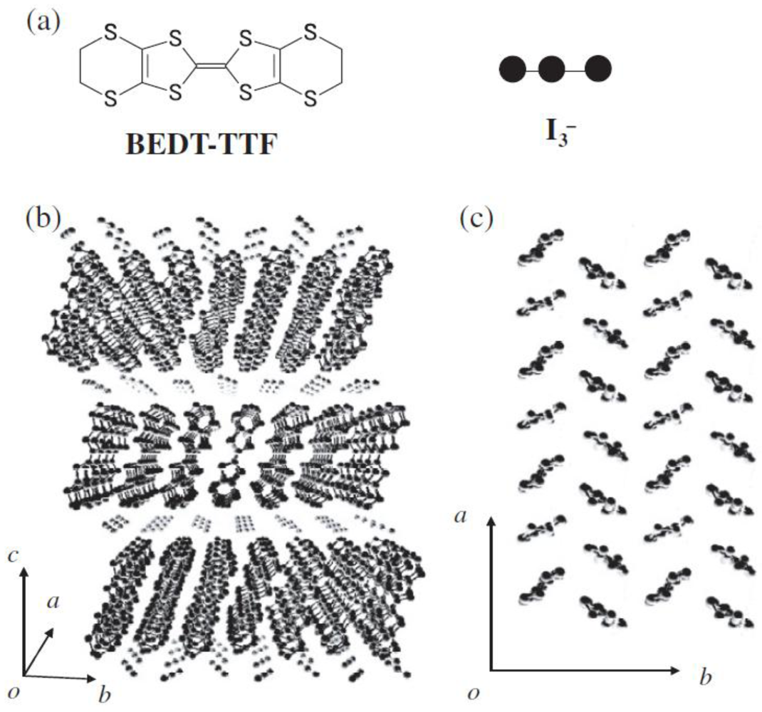
The organic conductor α-(BEDT-TTF)
2I
3 is a member of the (BEDT-TTF)
2I
3 family [
10]. All the crystals in this family consist of conductive layers of BEDT-TTF molecules and insulating layers of I
3− anions as shown in
Figure 1 [
10,
11,
12,
13]. The difference among them lies in the arrangement and orientation of BEDT-TTF molecules within the conducting plane, and this difference gives rise to variations in the transport phenomena. Most of the members of this family are 2D metals with large Fermi surfaces, and some of them are superconducting with
TC values of several Kelvin [
11,
12,
13]. On the other hand, α-(BEDT-TTF)
2I
3 is different from the other crystals. According to the band calculation, this system is a semimetal with two small Fermi surfaces; one with electron character and the other with hole character [
8].
Figure 1.
(
a) BEDT-TTF molecule and I
3− anion; (
b) Crystal structure of α-(BEDT-TTF)
2I
3 viewed from
a-axis; (
c) Crystal structure viewed from
c-axis. Reproduced with permission from [
5].
Figure 1.
(
a) BEDT-TTF molecule and I
3− anion; (
b) Crystal structure of α-(BEDT-TTF)
2I
3 viewed from
a-axis; (
c) Crystal structure viewed from
c-axis. Reproduced with permission from [
5].
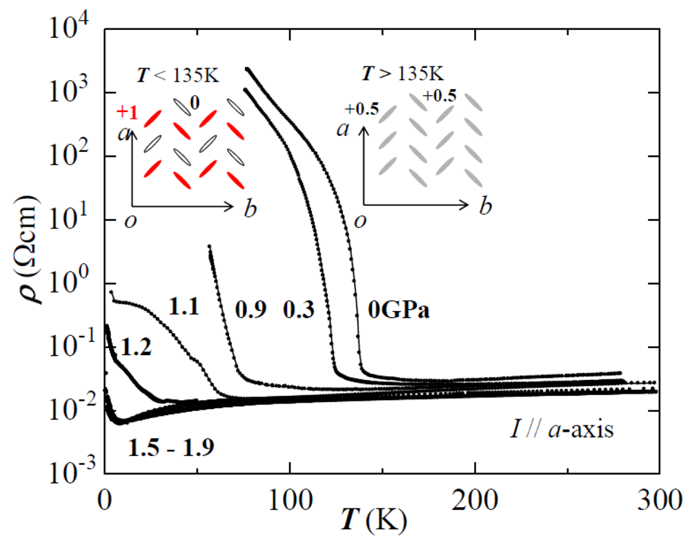
When cooled, it behaves as a metal above 135 K, where it undergoes a phase transition to an insulator as shown in
Figure 2 [
10]. In the insulator phase below 135 K, the rapid decrease in the magnetic susceptibility indicates that the system is in a nonmagnetic state with a spin gap [
14]. According to the theoretical work by Kino and Fukuyama [
15] and Seo [
16] and the experimental investigation by Takano
et al. (nuclear magnetic resonance) [
17], Wojciechowski
et al. (Raman) [
18] and Moldenhauer
et al. [
19], this transition is due to the charge disproportionation. In the metal state, the charge distribution of each BEDT-TTF molecules is approximately 0.5
e [
18,
20]. At temperatures below 135 K, however, horizontal charge stripe patterns for +1
e and 0 have been formed as shown in the inset of
Figure 2.
Figure 2.
Temperature dependence of the resistance under several hydrostatic pressures [
5,
8]. The inset shows a schematic picture of the arrangement of BEDT-TTF molecules in a conducting layer viewed from the
c-crystal axis and the charge pattern under ambient pressure. At temperatures below 135 K, the BEDT-TTF molecule layer forms horizontal charge stripe patterns for +1
e and 0 [
15,
16,
17,
18,
19]. Reproduced with permission from [
5].
When the crystal is placed under a high hydrostatic pressure of above 1.5 GPa, the metal-insulator transition is suppressed and the metallic region expands to low temperatures as shown in
Figure 2 [
7,
21,
22]. This change in the electronic state is accompanied by the disappearance of the charge-ordering state as shown by the Raman experiment [
18]. Note that in the high-pressure phase, the resistance is almost constant over the temperature region from 300 to 2 K. It looks like a dirty metal with a high density of impurities or lattice defects. In dirty metals, the mobilities of carriers are low and depend on temperature only weakly, and therefore, resistance is also independent of temperature. In the present case, however, the situation is different. Carriers with a very high mobility approximately 10
5 cm/V·s exhibit extremely large magnetoresistance at low temperatures [
5,
6,
7,
8,
21], indicating that the crystal is clean.
To clarify the mechanism of these apparently contradictory phenomena, the Hall effect was first examined by Mishima
et al. [
22]. However, the magnetic field of 5 T they used was too high to investigate the property of carriers in the zero-field limit. This is because the carrier system at low temperatures is sensitive to the magnetic field and its character is varied even in weak magnetic fields below 1 T. Thus, Tajima
et al. reexamined the Hall effect using a much lower magnetic field of 0.01 T [
8]. They also investigated the magnetoresistance and Hall resistance as a function of the magnetic field up to 15 T and the temperature between 0.5 and 300 K. The experimental results they obtained are summarized as follows: (1) Under a pressure of above 1.5 GPa, the resistivity is nearly constant between 300 and 2 K [
5,
8,
22]. (2) In the same region, both the carrier (hole) density and the mobility change by about six orders of magnitude as shown in
Figure 3. At low temperatures below 4 K, the carrier system is in a state with a low density of approximately 8 × 10
14 cm
−3 and a high mobility of approximately 3 × 10
5 cm
2/V·s [
5,
8]. (3) The effects of changes in the density and the mobility just cancel out to give a constant resistance [
5,
8,
22]. (4) At low temperatures, the resistance and Hall resistance are very sensitive to the magnetic field [
5,
7,
8,
21]. However, neither quantum oscillations nor the quantum Hall effect were observed in magnetic fields of up to 15 T [
5]. (5) The system is not a metal but a semiconductor with an extremely narrow energy gap of less than 1 meV [
5,
8].
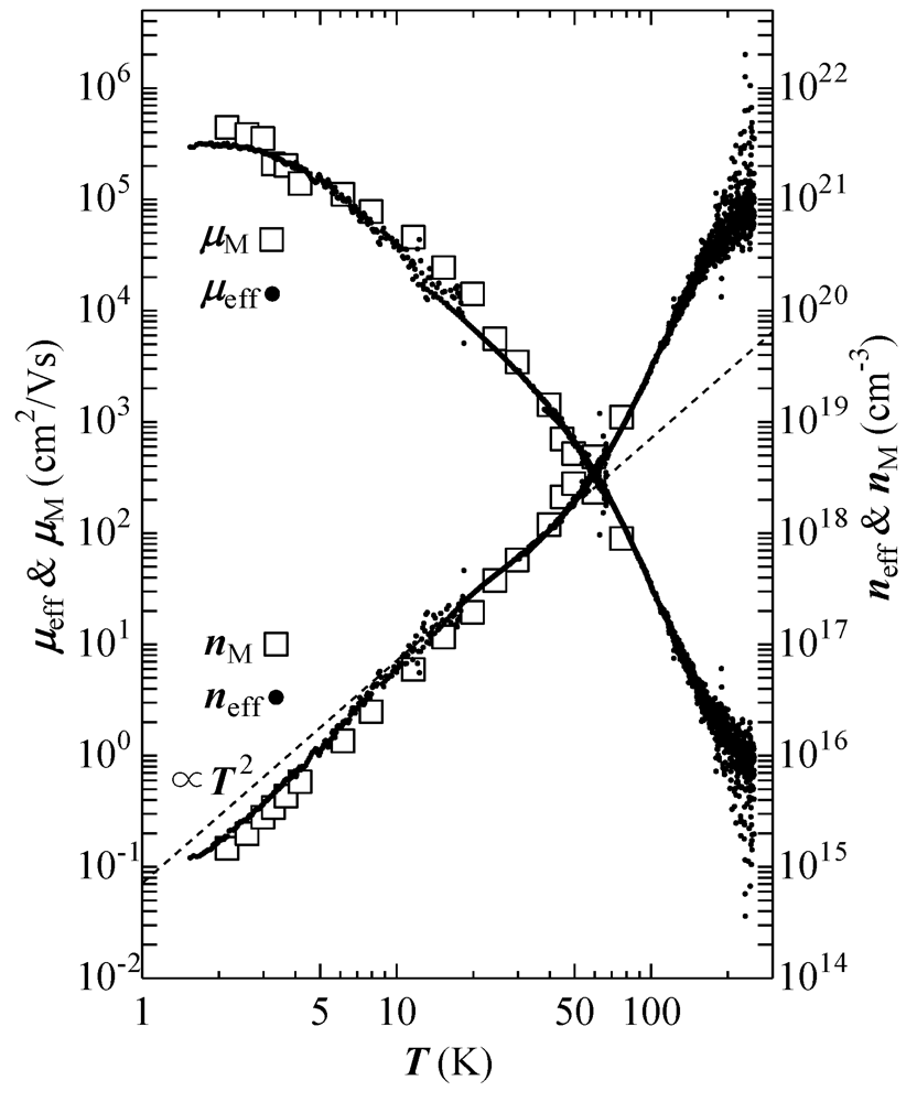
Figure 3.
Temperature dependence of the carrier density and the mobility for P= 1.8 GPa. The data plotted by close circle is the effective carrier density
neff and the mobility
μeff. The magnetoresistance mobility
μM and the density
nM, on the other hand, is shown by open square from 77 K to 2 K. The results of two experiments agree well and the density obeys
![Crystals 02 00643 i003]()
from 10 K to 50 K (indicated by broken lines). Reproduced with permission from [
5].
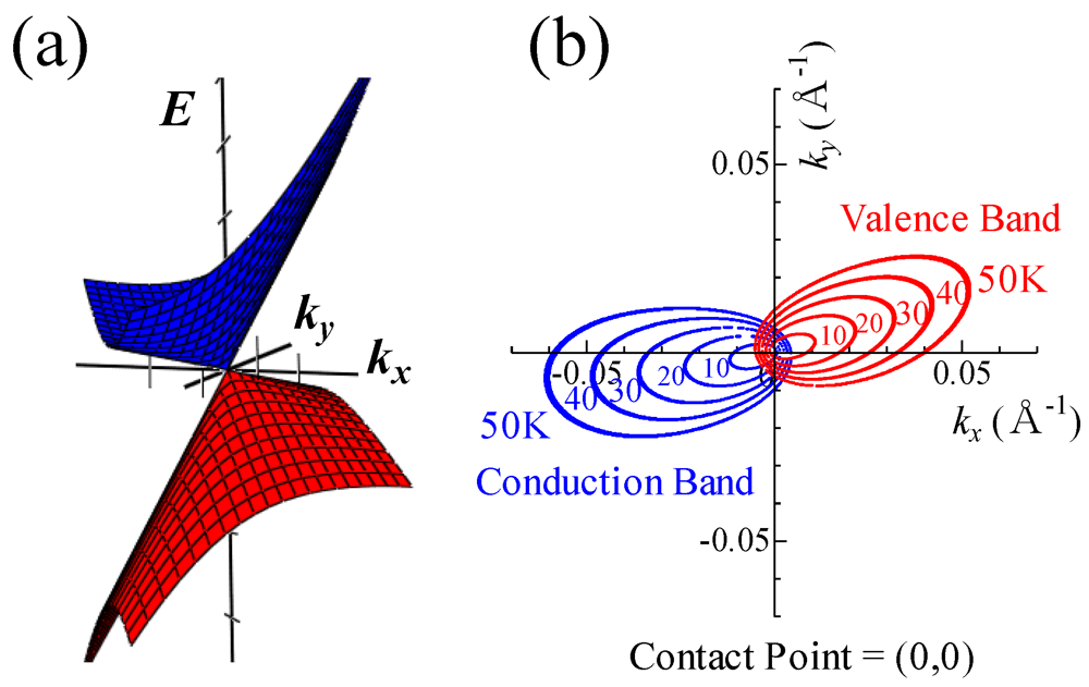
The mechanism of such anomalous phenomena, however, was not clarified until Kobayashi
et al. performed an energy band calculation in 2004 based on the crystal structure analysis of α-(BEDT-TTF)
2I
3 under uniaxial strain by Kondo and Kagoshima [
23] and suggested that this material under high pressures is in the zero-gap state [
3,
4]. According to their calculations, the bottom of the conduction band and the top of the valence band are in contact with each other at two points (we call these “Dirac points”) in the first Brillouin zone. The Fermi energy is located exactly on the Dirac point. In contrast to the case of graphene, in which the Dirac points are located at points in the
k-space with high symmetry, the positions of the Dirac points in the present system are unrestricted.
Figure 4 depicts the energy structure around one of the contact points. In the vicinity of the Dirac point, a Dirac cone type linear energy dispersion exists. It is expressed as
E = ±
hνF(
φ)(
k−
k0) where
νF(
φ) is the Fermi velocity and
k0 are the positions of the two contact points. As shown in
Figure 4, the present Dirac cone is slanted and has strong anisotropy. Therefore, the Fermi velocity
νF(
φ) depends on the direction of the vector (
k−
k0), which is denoted by
φ in the above equation. These results were supported by first-principles band calculations [
24].
The picture of the zero-gap system grow understanding of the remarkable transport phenomena of α-(BEDT-TTF)2I3. In this paper, we describe the interpretation of transport phenomena in this system based on the zero-gap picture.
Figure 4.
(
a) Band structure; and (
b) energy contours near a Dirac point. They are calculated using the parameters for P = 0.6 GPa in [
4]. Note that the origin of the axes is taken to be the position of the Dirac point. Reproduced with permission from [
6].
Figure 4.
(
a) Band structure; and (
b) energy contours near a Dirac point. They are calculated using the parameters for P = 0.6 GPa in [
4]. Note that the origin of the axes is taken to be the position of the Dirac point. Reproduced with permission from [
6].
2. Carrier Density, Mobility and Sheet Resistance
First, let us examine the temperature dependence of the carrier density shown in
Figure 3. Between 77 and 1.5 K, it decreases by about four orders of magnitude. This large reduction of the carrier density is characteristic of semiconductors. However, the temperature dependence is different from those of the ordinary semiconductors. In ordinary semiconductors with finite energy gaps, the carrier density depends exponentially on the inverse temperature. On the other hand, the data in
Figure 3 show a power-law-type temperature dependence
![Crystals 02 00643 i006]()
, with α ≈ 2. This temperature dependence of carrier density is explained on the basis of 2D zero-gap systems with a linear dispersion of energy. When we assumed the Fermi energy
EF is located at the contact point and does not move with temperature, this relationship is derived as
![Crystals 02 00643 i007]()
(1)
where
![Crystals 02 00643 i008]()
is the density of state for zero-gap structure,
f(E) is the Fermi distribution function,
C = 1.75 nm is the lattice constant along
c-axis and
![Crystals 02 00643 i009]()
is an average of
νF(
φ) defined by
![Crystals 02 00643 i010]()
. The averaged value of the Fermi velocity,
![Crystals 02 00643 i009]()
is estimated to be approximately 3 × 10
4 cm/s. This value corresponds to the result obtained from realistic theories [
4,
25].
Carrier mobility, on the other hand, is determined as follows. According to Mott's argument [
26], the mean free path
l of a carrier subjected to elastic scattering can never be shorter than the wavelength
λ of the carrier, so
l≤λ. For the cases in which scattering centers exist at high densities,
l~λ. As the temperature is decreased,
l becomes long because
λ becomes long with the decreasing energy of the carriers. As a result, the mobility of carriers increases in proportion to
T−2 in the 2D zero-gap system. Consequently, the Boltzmann transport equation gives the temperature independent quantum conductivity as
![Crystals 02 00643 i011]()
(2)
where νxx is the velocity of carriers on Dirac cone when the electric field is applied along x-axis and τ is the scattering lifetime, which is assumed to depend on the energy of the carriers.
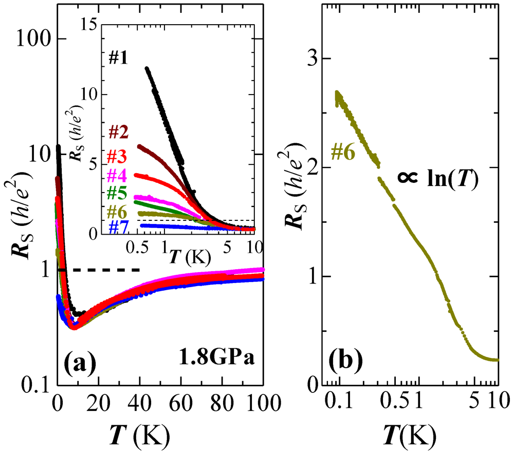
In order to examine Equation 2, we refer to
Figure 5 where the resistivity per layer (sheet resistance
Rs) for seven samples is plotted. Note that a conductive layer of this material is sandwiched by insulating layers as shown in
Figure 1, and therefore, each conductive layer is almost independent. Thus, the concept “resistivity per layer” is valid for this system. In this figure, it is shown that the sheet resistance depends on the temperature very weakly except for below 7 K. Note that the sheet resistance is close to the quantum resistance,
h/
e2 = 25.8 kΩ. It varies from a value approximately equal to the quantum resistance at 100 K to about 1/5 of it at 7 K. The reproducibility of data was checked using six samples. Many realistic theories predict that the sheet resistance of intrinsic zero-gap systems is given as
Rs =
gh/
e2, where
g is a parameter of order unity [
27,
28,
29]. Thus, the constant resistance observed in this material is ascribed to a zero-gap energy structure.
Figure 5.
(
a) Temperature dependence of
Rs for seven samples under a pressure of 1.8 GPa. The inset
Rs at temperatures below 10 K; (
b) Temperature dependence of
Rs for Sample 6. It was examined down to 80 mK. Reproduced with permission from [
30].
Figure 5.
(
a) Temperature dependence of
Rs for seven samples under a pressure of 1.8 GPa. The inset
Rs at temperatures below 10 K; (
b) Temperature dependence of
Rs for Sample 6. It was examined down to 80 mK. Reproduced with permission from [
30].
Here, we mention the resistivity below 7 K in
Figure 5. The sample dependence due to the effects of unstable I
3− anions appears strongly. A rise of
Rs may be a symptom of localization because it is proportional to log
T as shown in the inset of
Figure 5a. The unstable I
3− gives rise to a partially incommensurate structure in the BEDT-TTF layers. As for Sample 6, the log
T law of
Rs was examined down to 80 mK. The log
T law of resistivity, on the other hand, is also characteristic of the transport of Kondo-effect systems. In graphene, recently, Chen
et al. have demonstrated that the interaction between the vacancies and the electrons give rise to Kondo-effect systems [
31]. The origin of the magnetic moment was the vacancy. In α-(BEDT-TTF)
2I
3, on the other hand, Kanoda
et al. detected anomalous NMR signals which could not be understood based on the picture of Dirac fermion systems at low temperatures [
32]. We do not yet know whether, in the localization, the Kondo-effect or other mechanisms are the answer for the origin of the log
T law of
Rs. This answer, however, will answer the question as to why the sample with the higher carrier density (lower
RH saturation value in
Figure 6) exhibits the higher
Rs at low temperature. Further investigation should lead us to interesting phenomena.
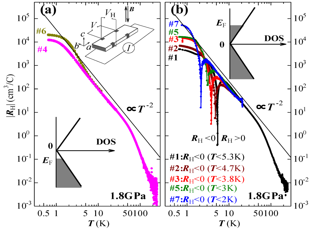
Figure 6.
Temperature dependence of the Hall coefficient for (
a) hole-doped-type; and (
b) electron-doped-type samples. Note that in this figure, the absolute value of
RH is plotted. Thus, the dips in (
b) indicate a change in the polarity. The inset in the upper part of (
a) shows the configuration of the six electrical contacts. The schematic illustration of the Fermi levels for the hole-doped type and the electron-doped type are shown in the inset in the lower part of (
a) and the inset of (
b), respectively. Reproduced with permission from [
30].
Here we adduce other examples for the effect of unstable I
3− anions. It was also seen in the superconducting transition of the organic superconductors β-(BEDT-TTF)
2I
3 [
33] and θ-(BEDT-TTF)
2I
3 [
34].
In conclusion of this section, α-(BEDT-TTF)
2I
3 under high hydrostatic pressure is an intrinsic zero-gap system with Dirac type energy band
E = ±
hνF(
φ)(
k −
k0). In the graphite systems, a monolayer sample (graphene) is inevitable to realize a zero-gap state. On the other hand, in the present system, bulk crystals can be two dimensional zero-gap systems. The carrier density depends on temperature as
![Crystals 02 00643 i003]()
. On the other hand, the resistance remains constant in the wide temperature region. The value of the sheet resistance coincide the quantum resistance
h/
e2 = 25.8 kΩ within a factor of 5.
3. Inter-Band Effects of the Magnetic Field
A magnetic field gives us characteristic phenomena. According to the theory of Fukuyama, the vector potential plays an important role in inter-band excitation in electronic systems with a vanishing or narrow energy gap [
35]. The orbital movement of virtual electron-hole pairs gives rise to anomalous orbital diamagnetism and the Hall effect in a weak magnetic field. These are called the interband effects of the magnetic field. This discovery inspired us to examine the interband effects of the magnetic field in α-(BEDT-TTF)
2I
3. In this section, we demonstrate that these effects give rise to anomalous Hall conductivity in α-(BEDT-TTF)
2I
3. Bismuth and graphite are the most well-known materials that serve as testing ground for the interband effects of magnetic fields. To our knowledge, however, α-(BEDT-TTF)
2I
3 is the first organic material in which the inter-band effects of the magnetic field have been detected.
Realistic theory predicts that the interband effects of the magnetic field are detected by measuring the Hall conductivity
σxy or the magnetic susceptibility at the vicinity of the Dirac points [
35,
36]. In order to detect these effects, we should control the chemical potential
μ. In this material, however, the multilayered structure makes control of
μ by the field-effect-transistor method much more difficult than in the case of graphene. Hence, we present the following idea.
We find two types of samples in which electrons or holes are slightly doped by unstable I
3− anions. The doping gives rise to strong sample dependences of the resistivity or the Hall coefficient at low temperatures (
Figure 5 and
Figure 6). In particular, the sample dependence of the Hall coefficient
RH is intense. In the hole-doped sample as shown in the inset of the lower part of
Figure 6a,
RH is positive over the whole temperature range (
Figure 6a). In the electron-doped sample as shown in the inset of
Figure 6b, however, the polarity is changed at low temperatures (
Figure 6b). The change in polarity of
RH is understood as follows. In contrast to graphene, the present electron-hole symmetry is not good except at the vicinity of the Dirac points [
24]. Thus,
μ must be dependent on temperature. Of significance is the fact that according to the theory by Kobayashi
et al., when
![Crystals 02 00643 i014]()
passes the Dirac point (
μ = 0),
RH = 0 [
36]. Thus,
RH at the vicinity of
RH = 0 for electron-doped samples must be determined to detect the inter-band effects of the magnetic field. The saturation value of
RH at the lowest temperature, on the other hand, depends on the doping density
nd, as
nd =
ns/
C = 1/(
eRH), where
ns is the sheet density.
nd =
ns/
C = 1/(
eRH).
Note that the carrier density and the mobility in
Figure 3 is the behavior for hole-doped type sample. However, the temperature dependence of
μ is much weaker than the thermal energy and the doping levels are estimated to be several ppm. Thus, the relationship of Equation 1 is valid which is derived when we assumed that
μ locates at the Dirac point and does not move with the temperature, in
Section 2.
In this section, thus, to detect the inter-band effects of the magnetic field, we focused on the behavior of
RH in which the polarity is changed (
Figure 6b). It was examined as follows.
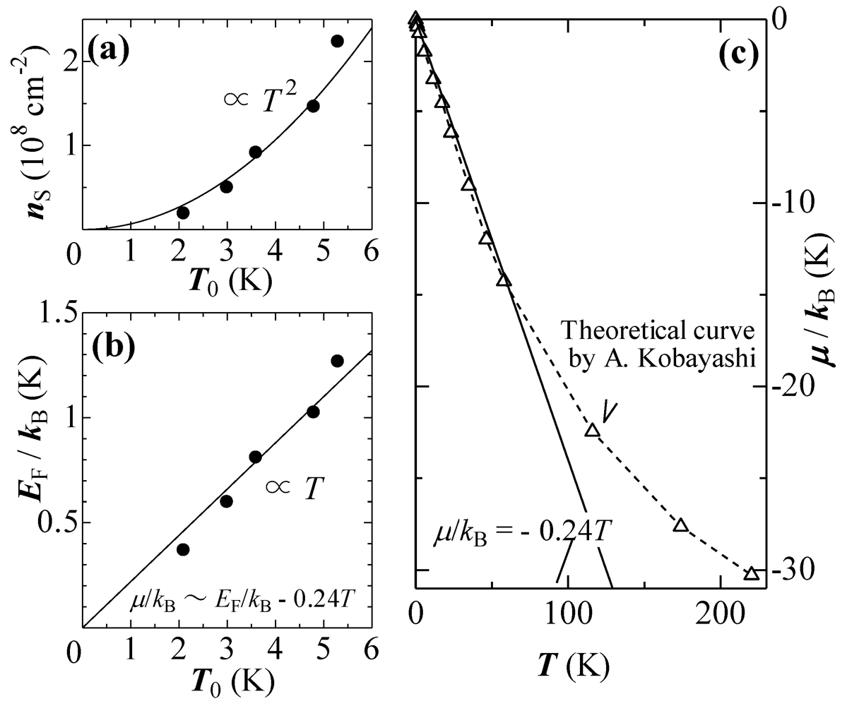
The first step is to examine the temperature dependence of
μ. As mentioned before, we believe
μ passes the Dirac point at the temperature
T0, shown as
RH = 0 [
36]. The sheet density
ns, on the other hand, is approximately proportional to
T02 as shown in
Figure 7(a). This result suggests that
μ is to be written as
μ/
kB =
EF/
kB−
AT at
T0 approximately because
![Crystals 02 00643 i015]()
, where
A is the fitting parameter depending on the electron-hole symmetry (
![Crystals 02 00643 i016]()
). Thus, we obtain the
EF versus
T0 curve in
Figure 7b.
EF is estimated from the relationship
ns =
EF2/(4π
h2νF2), where the averaged Fermi velocity
νF, is estimated to be approximately 3.3 × 10
4 m/s from the temperature dependence of the carrier density. Note that the weak sample dependence of both
Rs and
RH at temperatures above 7 K (
Figure 5 and
Figure 6) strongly indicates that the
νF values of all samples are almost the same. When we assume that
A is independent of
EF,
A is estimated to be approximately 0.24 from
Figure 7b. Thus, we examine the temperature dependence of
μ as
μ/
kB =
EF/
kB−
AT with
A ~ 0.24. This experimental formula reproduces well the realistic theoretical curve by Kobayashi
et al. [
36], as shown in
Figure 7(c). Our simple calculations, on the other hand, also reproduce well this curve when we assume
![Crystals 02 00643 i017]()
, where
![Crystals 02 00643 i018]()
and
![Crystals 02 00643 i019]()
are the Fermi velocities for lower and upper Dirac cones, respectively. This is the electron-hole asymmetry in this system. Actually, the result of the first principle band calculation by Kino and Miyazaki indicate that the electron-hole symmetry is not complete [
24].
Figure 7.
(
a) Sheet electron density
ns for five samples plotted against temperature at
RH. (
b)
EF was estimated from the relationship
ns =
EF2/(4π
h2νF2) with
νF ~ 3.3 × 10
4 m/s. From this curve, the temperature dependence of
μ is written approximately as
μ/
kB =
EF/
kB−
AT with
A ~ 0.24 when we assume
A is independent of
EF. (
c) Temperature dependence of
μ for
EF = 0. Our experimental formula is quantitatively consistent with the theoretical curve of Kobayashi
et al. [
36] at temperature below 100 K. Reproduced with permission from [
30].
The second step is to calculate the Hall conductivity as
σxy =
ρyx/(
ρxxρyy +
ρyx2). In this calculation, we assume
ρxx =
ρyy for the following reasons. According to band calculation, the energy contour of the Dirac cone is highly anisotropic [
4]. In the galvano-magnetic phenomena, however, the anisotropy is averaged and the system looks very much isotropic. A simple calculation indicates that the variation in the mobility with the current direction is within a factor of 2. Experimentally, Iimori
et al. showed that the anisotropy in the in-plane conductivity is less than 2 [
37].
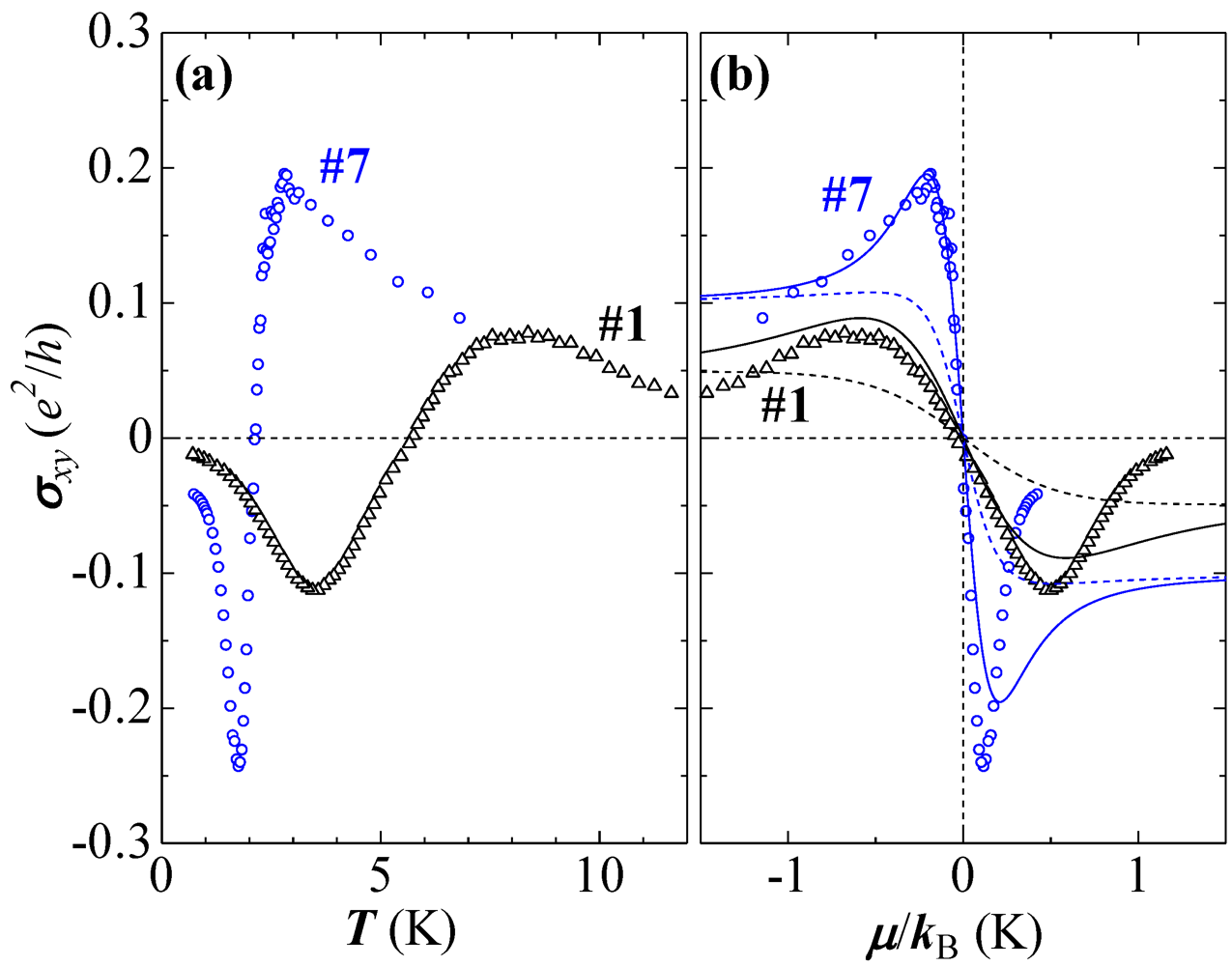
Based on this assumption, we show the temperature dependence of
σxy for Samples 1 and 7 in
Figure 5 and
Figure 6 in
Figure 8a as an example. We see the peak structure in
σxy at the vicinity of
σxy = 0. This peak structure is the anomalous Hall conductivity originating from the interband effects of the magnetic field. The realistic theory indicates that the Hall conductivity without the interband effects of the magnetic field has no peak structure [
36].
In the last step, we redraw
σxy in
Figure 8b as a function of
μ using the experimental formula,
μ/
kB =
EF/
kB −
AT with
A = 0.24. It should be compared with the theoretical curve [
36],
![Crystals 02 00643 i021]()
at
T = 0. Our experimental data are roughly expressed as
![Crystals 02 00643 i022]()
, where
g is a parameter that depends on temperature because the effect of thermal energy on the Hall effect is strong. Note that
σxy depends strongly on temperature. The energy between two peaks is the damping energy that depends on the density of scattering centers in a crystal. The intensity of the peak, on the other hand, depends on the damping energy and the tilt of the Dirac cones [
36].
Figure 8.
(
a) Temperature dependence of the Hall conductivity for Samples 1 and 7 in
Figure 5 and
Figure 6; (
b) Chemical-potential dependence of the Hall conductivity for Samples 1 and 7. Solid lines and dashed lines are the theoretical curves with and without the interband effects of the magnetic field by Kobayashi
et al., respectively [
36]. Reproduced with permission from [
30].
Lastly, we briefly mention the zero-gap structure in this material. The smooth change in the polarity of
σxy is also evidence that this material is an intrinsic zero-gap conductor. Nakamura demonstrated theoretically that in a system with a finite energy gap,
σxy is changed in a stepwise manner at the Dirac points [
38].
In conclusion of this section, we succeeded in detecting the interband effects of the magnetic field on the Hall conductivity when μ passes the Dirac point. Good agreement between experiment and theory was obtained.
4. Effects of Zero-Mode Landau Level on Transport
One of the characteristic features in Dirac fermion system is clearly seen in the magnetic field. In this section, the transport phenomena in the magnetic field are described. Note that we interpret the transport phenomena based on the assumption which EF locates at the Dirac point because EF is lower than broadening energy of Landau levels.
In the magnetic field, the energy of Landau levels (LLs) in zero-gap systems is expressed as
![Crystals 02 00643 i024]()
, where
n is the Landau index and
B is the magnetic field strength [
39]. One important difference between zero-gap conductors and conventional conductors is the appearance of a (
n = 0) LL at zero energy when magnetic fields are applied normal to the 2D plane. This special LL is called the zero-mode. Since the energy of this level is
EF irrespective of the field strength, the Fermi distribution function is always 1/2. It means that half of the Landau states in the zero mode are occupied. Note that in each LL, there are states whose density is proportional to
B. The magnetic field, thus, creates mobile carriers.
For kBT < E1LL, most of the mobile carriers are in the zero-mode. Such a situation is called the quantum limit. The carrier density per valley and per spin direction in the quantum limit is given by D(B) = B/2φ0, where φ0 = h/e is the quantum flux. The factor 1/2 is the Fermi distribution function at EF. In moderately strong magnetic fields, the density of carriers induced by the magnetic field can be very high. At 3 T, for example, the density of zero-mode carriers will be 1015 m−2. This value is by about 2 orders of magnitude higher than the density of thermally excited carriers at 4 K, and, in the absence of the magnetic field, it is 1013 m−2. Therefore, carrier density in the magnetic field is expressed as B/2φ0 except for very low fields.
This effect is detected in the inter-layer resistance,
Rzz, in the longitudinal magnetic field. In this field configuration, the interaction between the electrical current and the magnetic field is weak because they are parallel to each other. Hence, the effect of the magnetic field appears only through the change in the carrier density. In this regard, the large change in the density of zero-mode carriers gives rise to remarkable negative magnetoresistance in the low magnetic field region, as shown in
Figure 9 [
40,
41].
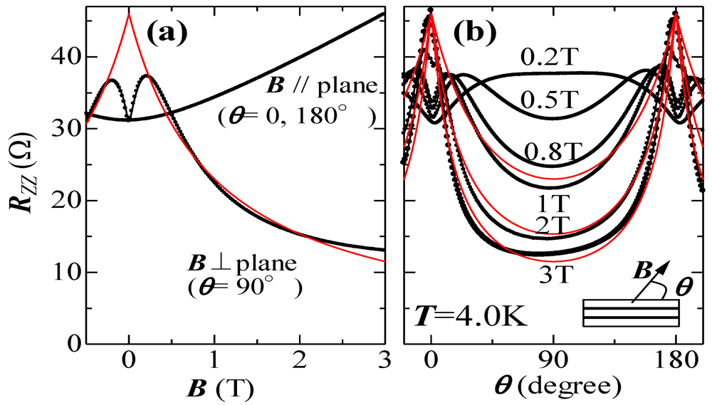
Figure 9.
(
a) Magnetic field dependence of interlayer resistance under the pressure about 1.7 GPa at 4 K. When
B > 0.2 T, remarkable negative magnetoresistance is observed. As for negative magnetoresistance, fitting is done with Equation 3,
![Crystals 02 00643 i025]()
(red line); (
b) Angle dependence of magnetoresistance. When
θ = 0 and
θ = 180°, the direction of the magnetic field is parallel to the 2D plane.
θ = 90° is the direction normal to the 2D plane. Fitting of the data measured at 1, 2, and 3 T was done using Equation 3. Reproduced with permission from [
40].
Recently, Osada gave an analytical formula for interlayer magnetoresistance in a multilayer Dirac fermion system as follows:
![Crystals 02 00643 i027]()
(3)
where
A = π
h3/2
C'tc2ce3 is a parameter that is considered to be independent of the magnetic field if the system is clean.
B0 is a fitting parameter that depends on the quality of the crystal,
C' is defined by
![Crystals 02 00643 i028]()
using the spectral density of the zero-mode Landau level and
ρ0(
E) satisfies
![Crystals 02 00643 i029]()
[
42].
Except for narrow regions around
θ = 0 and
θ = 180°, this formula can be simplified to
Rzz =
A/(|
B| +
B0). Using this formula and assuming
B0 = 0.7 T, we tried to fit the curves in
Figure 9. This simple formula reproduces well both the magnetic field dependence and the angle dependence of the magnetoresistance at magnetic fields above 0.5 T as shown by solid lines in
Figure 9, which evidences the existence of zero-mode Landau carriers in α-(BEDT-TTF)
2I
3 at high pressures.
Here, we briefly mention the origin of positive magnetoresistance around
θ = 0 and
θ = 180°. In the magnetic field in these directions, the Lorentz force works to bend the carrier trajectory to the direction parallel to the 2D plane. It reduces the tunneling of carriers between neighboring layers so that the positive magnetoresistance is observed. Note that the Equation 3 for
θ = 0 and
θ = 180° dose not correctly evaluate the effect of the Lorentz force and, thus, loses its validity. The value of the resistance peak depends weakly on the azimuthal angle. At 3 T, for example, the ratio of maximum value to the minimum value is less than 1.3. According to the calculation of interlayer magnetoresistance by Morinari, Himura and Tohyama, the effect of Dirac cones with highly anisotropic Fermi velocity is averaged and gives rise to this small difference [
43].
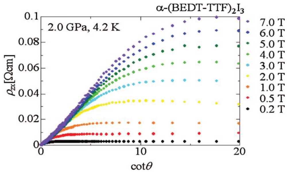
Angle dependence of interlayer Hall resistivity
ρzx in the fixed magnetic field gives also us the characteristic phenomena in quantum limit state [
44,
45].
Figure 10 shows cot
θ dependence of inter-layer Hall resistivity
ρzx in the magnetic field below 7 T at 4.2 K. We find the relationship of
ρzx=Acot
θ, where slope
A is close to the quantum resistance,
h/
e2 = 25.8 kΩ and is independent of the magnetic field. This is simply understood as follows. In general, Hall voltage is proportional to cos
θ. Thus, angle dependence of interlayer Hall resistivity is written as
ρzx =
ρ0 cos
θ =
B/ne cos
θ. The degeneracy of zero-mode, on the other hand, is proportional to the magnetic field, and then
n =
B/2
φ0 sin
θ. Thus, we obtain the relationship
ρzx =
h/2
e2 cot
θ.
Figure 10.
cot
θ dependence of inter-layer Hall resistivity
ρzx at 4.2 K. When the magnetic field is applied along to 2D plane,
θ = 0 or
θ = 180°. Reproduced with permission from [
44].
Figure 10.
cot
θ dependence of inter-layer Hall resistivity
ρzx at 4.2 K. When the magnetic field is applied along to 2D plane,
θ = 0 or
θ = 180°. Reproduced with permission from [
44].
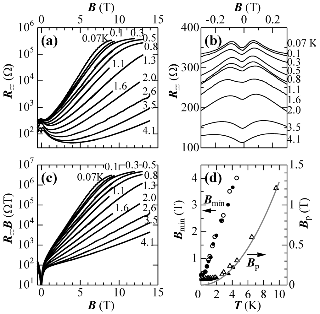
Here, let us return to
Figure 9. An apparent discrepancy from Equation 3 of the data is also seen at both low and high magnetic fields normal to the 2D plane, because the model is oversimplified. Equation 3 was derived based on the quantum limit picture in which only the zero-mode LL is considered. In fact, each LL has a finite width due to scattering. At a sufficiently low magnetic field, the zero-mode LL overlaps with other Landau levels. In such a region, Equation 3 loses its validity. We can recognize this region in
Figure 9 below 0.2 T, where positive magnetoresistance is observed. This critical magnetic field,
Bp, shifts to a lower field with decreasing temperature, where it almost saturates at about 0.04 K, as shown in
Figure 11b,d.
Figure 11.
(
a) Magnetic field dependence of
Rzz below 4.1 K under pressure of approximately 1.7 GPa; (
b)
Rzz in the low field region below 0.4 T; (
c) Magnetic field dependence of
Rzz B; (
d) Temperature dependence of
Bp (solid triangles) and
Bmin (solid circles). The solid line is the curve of
E1LL with
νF ~ 4 ×10
4 m/s. Reproduced with permission from [
41].
The overlap between the zero-mode and other LLs, primarily the
n = 1 LL will be sufficiently small above
Bp and as a result, the negative magnetoresistance is observed there. Then, we have a tentative relationship:
E1LL ~ 2
kBTp at
Bp [
41,
46]. In fact,
E1LL with
νF ~ 4 × 10
4 m/s is reproduced well except in the temperature region below 2 K. This Fermi velocity corresponds to that estimated from the temperature dependence of the carrier density [
6]. The discrepancy of the data from the curve of
E1LL below 2 K, on the other hand, suggests that thermal energy is sufficiently lower than the scattering broadening energy г
0. Thus, г
0 is roughly estimated to be approximately 2 K from the constant value of
Bp as
![Crystals 02 00643 i032]()
at 0.1 T [
41,
46]. This scattering broadening energy is much lower than that of graphene. In graphene, г
0 was estimated to be about 30 K.
The deviation from Equation 3 of data in the high field region of
Figure 9 is much more serious. In this region, the resistance increases exponentially with increasing field. This phenomenon is understood as follows.
In the above discussion, we did not consider the Zeeman effect. The Zeeman effect, however, should be taken into consideration because it has a significant influence on the transport phenomena at low temperatures. In the presence of a magnetic field, each LL is split into two levels with energies
EnLL = ±Δ
E, where Δ
E =
μBB is the Zeeman energy. This change in the energy structure gives rise to a change in the carrier density in LLs. In particular, the influence on the zero-mode carrier density is the strongest, because the energy level is shifted from the position of the Fermi energy. The value of the Fermi distribution function varies from
f(
EF) = 1/2 to
f(Δ
E) = 1/(exp(Δ
E/
kBT) + 1). At low temperatures where
kBT < Δ
E , this effect becomes important. It works to reduce the density of zero-mode carriers and, thus, increases the resistance as
![Crystals 02 00643 i033]()
(
Figure 11 a,c) [
38,
39]. According to the theory of Osada, on the other hand,
μBB ~ г
0 at the magnetoresistance minimum [
42].
The Zeeman energy when
B = 1 T is about 1 K. Therefore, in the experiment performed at 1 K, the deviation of experimental results from Equation 3 is expected to start around 1 T. This is confirmed in
Figure 11a. We find a resistance minimum. At 1.8 K, for example, the deviation is prominent in fields above 2 T. This critical field shifts to about 0.3 T at 0.07 K.
Recently, Osada pointed out the possibility of
ν = 0 quantum Hall effect (QHE) in this region [
47]. In the spin-splitting state of 2D Dirac fermion system such as graphene, the edge state with a pair of inverse spins exists at near the edge of sample as shown in
Figure 12. According to the theory by Osada [
47], the saturation of data at low temperatures and high magnetic fields in
Figure 11a strongly indicates the existence of the edge state. Thus,
ν= 0 quantum Hall state is expected in this region. Note that in this special state, the characteristic in-plane transport (
σxx and
σxy) phenomena in conventional quantum Hall state is not detected.
Figure 12.
Edge state Spector in ν = 0 quantum Hall state.
Figure 12.
Edge state Spector in ν = 0 quantum Hall state.
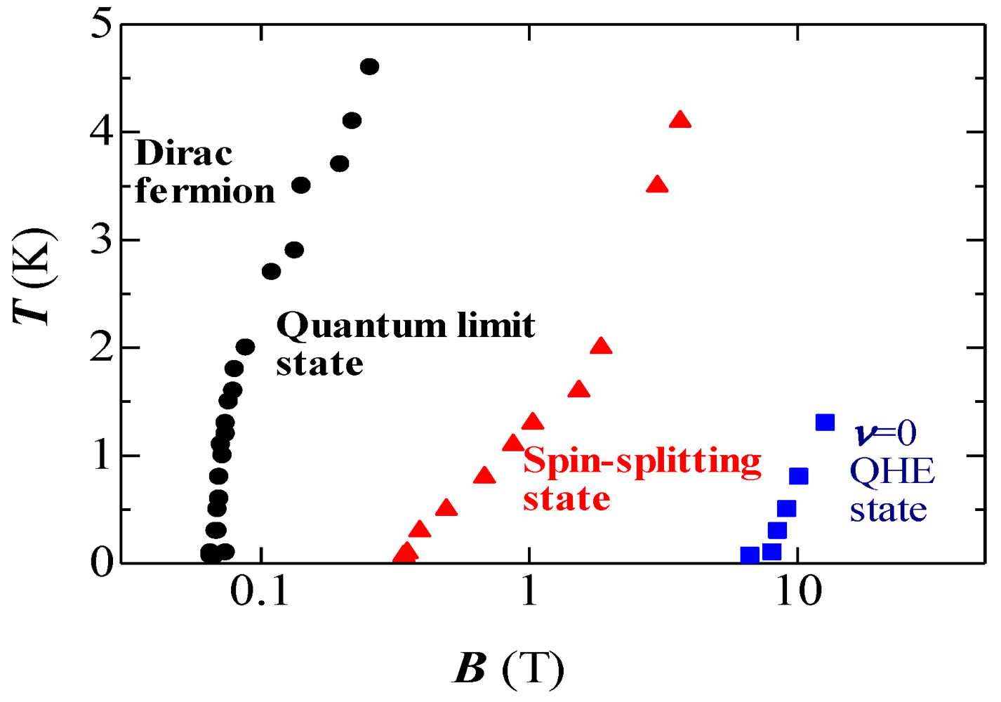
In conclusion of this section, we succeeded in detecting the zero-mode Landau level. The characteristic feature of zero-mode Landau carriers including the Zeeman effect was clearly seen in the inter-layer transport. The experimental data suggest that with increasing magnetic field or decreasing temperature, the system changes from a “Dirac fermion” state to a “quantum limit state”, then to a “spin-splitting” state and then to a “
ν = 0 QHE” state as shown in
Figure 13, where the boundaries between the states in the
B–
T plane are depicted using the data in
Figure 11. Stepwise changes in the states between boundaries, on the other hand, are observed in in-plane magnetoresistance as shown in
Figure 14.
Figure 13.
Schematic diagram of boundaries in
B–
T plane depicted using the data in
Figure 11. “Dirac fermion” state is the low magnetic field region, “quantum limit” state is the region observed negative magnetoresistance, the region that obeyed an exponential law is “spin-splitting” state and “
ν = 0 quantum Hall effect” state is the saturation region at low temperature and high magnetic field.
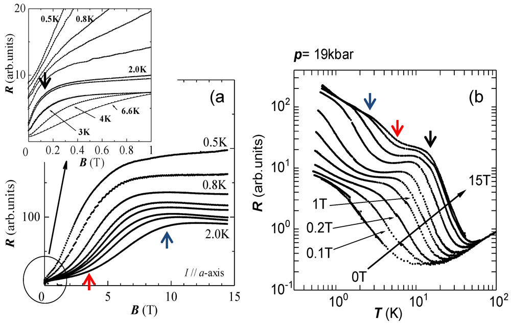
Figure 14.
(
a) Magnetic field dependence of the in-plane resistance down to 0.5 K. The low-field region below 1 T is shown in the inset; (
b) Temperature dependence of the in-plane resistance under a magnetic field of up to 15 T. The arrows shows the boundaries between “Dirac fermion”, “quantum limit”, “spin-splitting” and “
ν = 0 quantum Hall effect” states. Reproduced with permission from [
5].


 from 10 K to 50 K (indicated by broken lines). Reproduced with permission from [5].

 , with α ≈ 2. This temperature dependence of carrier density is explained on the basis of 2D zero-gap systems with a linear dispersion of energy. When we assumed the Fermi energy EF is located at the contact point and does not move with temperature, this relationship is derived as
  (1)
(1)  is the density of state for zero-gap structure, f(E) is the Fermi distribution function, C = 1.75 nm is the lattice constant along c-axis and
  is an average of νF(φ) defined by
  . The averaged value of the Fermi velocity,
  (2)
(2) 

 passes the Dirac point (μ = 0), RH = 0 [36]. Thus, RH at the vicinity of RH = 0 for electron-doped samples must be determined to detect the inter-band effects of the magnetic field. The saturation value of RH at the lowest temperature, on the other hand, depends on the doping density nd, as nd = ns/C = 1/(eRH), where ns is the sheet density. nd = ns/C = 1/(eRH).
 , where A is the fitting parameter depending on the electron-hole symmetry (
  ). Thus, we obtain the EF versus T0 curve in Figure 7b. EF is estimated from the relationship ns = EF2/(4πh2νF2), where the averaged Fermi velocity νF, is estimated to be approximately 3.3 × 10⁴ m/s from the temperature dependence of the carrier density. Note that the weak sample dependence of both Rs and RH at temperatures above 7 K (Figure 5 and Figure 6) strongly indicates that the νF values of all samples are almost the same. When we assume that A is independent of EF, A is estimated to be approximately 0.24 from Figure 7b. Thus, we examine the temperature dependence of μ as μ/kB = EF/kB− AT with A ~ 0.24. This experimental formula reproduces well the realistic theoretical curve by Kobayashi et al. [36], as shown in Figure 7(c). Our simple calculations, on the other hand, also reproduce well this curve when we assume
  , where
  and
and  are the Fermi velocities for lower and upper Dirac cones, respectively. This is the electron-hole asymmetry in this system. Actually, the result of the first principle band calculation by Kino and Miyazaki indicate that the electron-hole symmetry is not complete [24].
 at T = 0. Our experimental data are roughly expressed as
  , where g is a parameter that depends on temperature because the effect of thermal energy on the Hall effect is strong. Note that σxy depends strongly on temperature. The energy between two peaks is the damping energy that depends on the density of scattering centers in a crystal. The intensity of the peak, on the other hand, depends on the damping energy and the tilt of the Dirac cones [36].
 , where n is the Landau index and B is the magnetic field strength [39]. One important difference between zero-gap conductors and conventional conductors is the appearance of a (n = 0) LL at zero energy when magnetic fields are applied normal to the 2D plane. This special LL is called the zero-mode. Since the energy of this level is EF irrespective of the field strength, the Fermi distribution function is always 1/2. It means that half of the Landau states in the zero mode are occupied. Note that in each LL, there are states whose density is proportional to B. The magnetic field, thus, creates mobile carriers.
  (red line); (b) Angle dependence of magnetoresistance. When θ = 0 and θ = 180°, the direction of the magnetic field is parallel to the 2D plane. θ = 90° is the direction normal to the 2D plane. Fitting of the data measured at 1, 2, and 3 T was done using Equation 3. Reproduced with permission from [40].

 (3)
(3)  using the spectral density of the zero-mode Landau level and ρ0(E) satisfies
  [42].
[42]. 

 at 0.1 T [41,46]. This scattering broadening energy is much lower than that of graphene. In graphene, г0 was estimated to be about 30 K.
 (Figure 11 a,c) [38,39]. According to the theory of Osada, on the other hand, μBB ~ г0 at the magnetoresistance minimum [42].
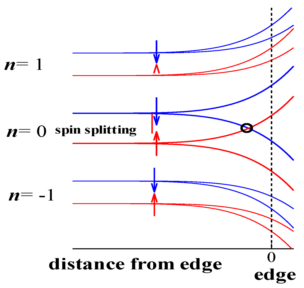
 , is a characteristic feature of the zero-gap system. On the other hand, the resistance remains constant from 2 to 300 K. The sheet resistance can be written in terms of the quantum resistance h/e2 as Rs = gh/e2, where g is a parameter that depends weakly on temperature. Moreover, we succeeded in detecting the interband effects of the magnetic field on the Hall conductivity when the chemical potential passes the Dirac point. In graphite systems, a monolayer sample (graphene) is necessary to realize a zero-gap state. On the other hand, in the present system, it was demonstrated that bulk crystals can be 2D zero-gap systems. We can observe this effect in the inter-layer magnetoresistance. The existence of the zero-mode Landau level is one of characteristic features in the zero-gap system. The effect of Landau degeneracy, which is proportional to the strength of the magnetic field, gives rise to the large negative magnetoresistance. We anticipate the ν = 0 quantum Hall state in the spin-splitting state of zero-mode at low temperature and high magnetic field. Lastly, we mention the robustness of zero-gap structure in this compound. The temperature dependence of the carrier density that ruled out