
High-Efficiency Broadband Selective Photothermal Absorbers Based on Multilayer Chromium Films

 ,
,  , ,
, , 

Abstract
1. Introduction
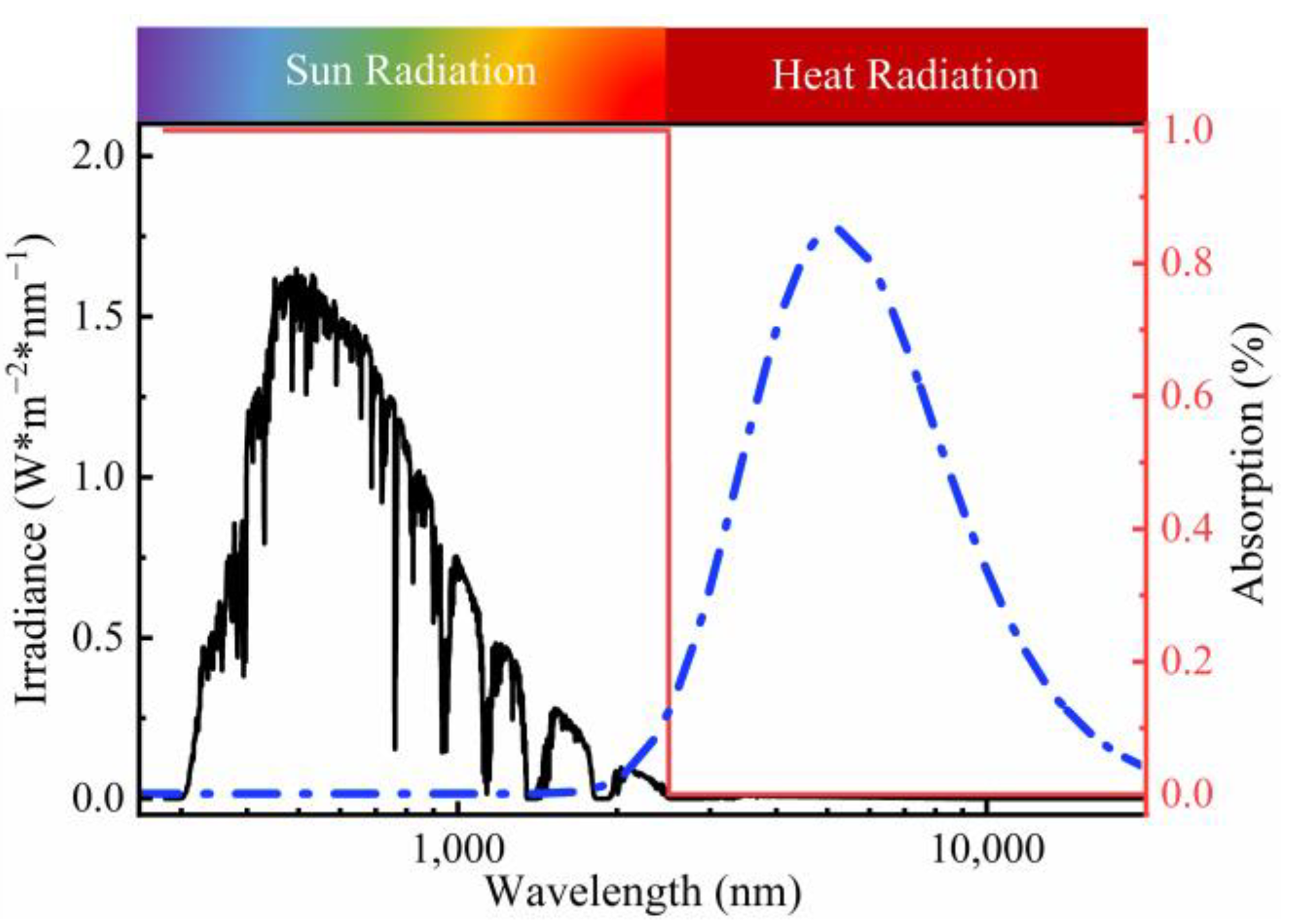
2. Principle
3. Structure and Simulation
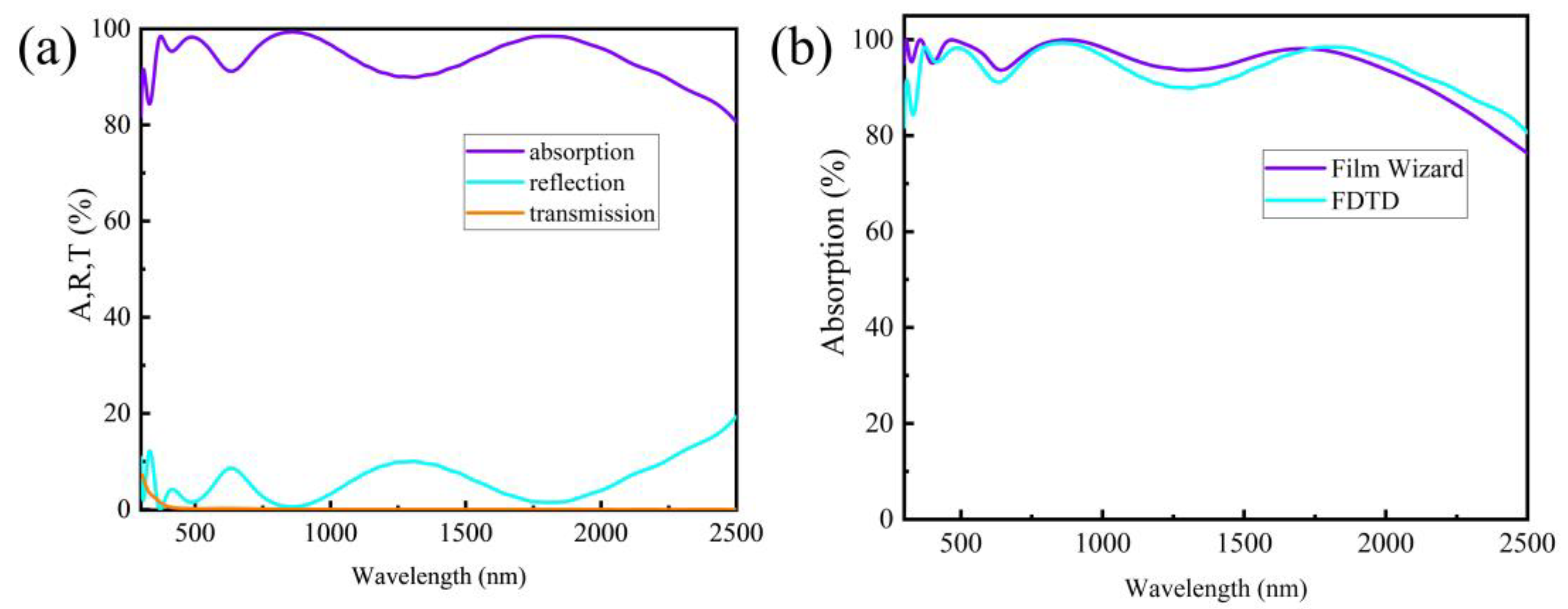
3.1. Multilayer Structure and Numerical Simulation Results
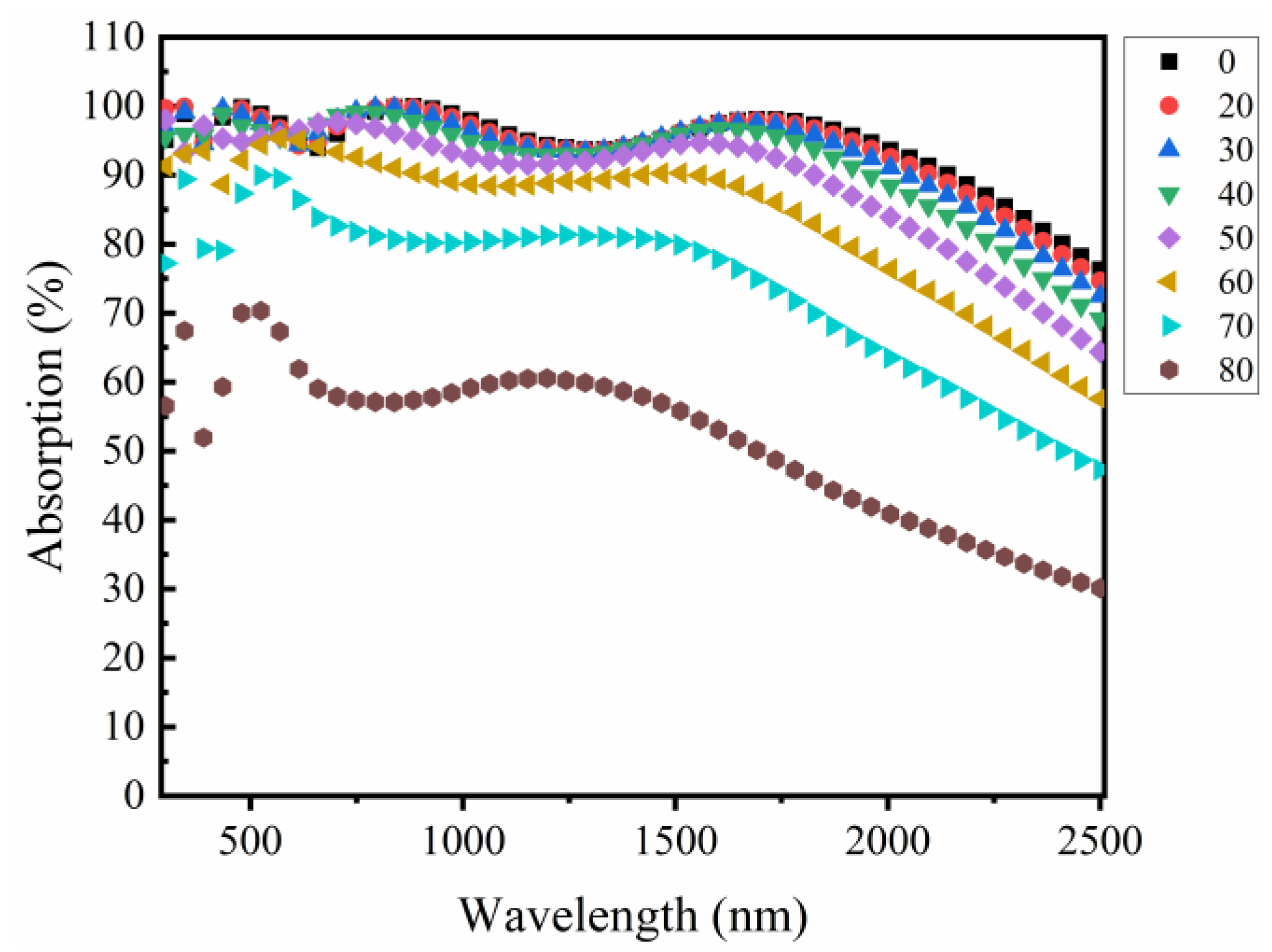
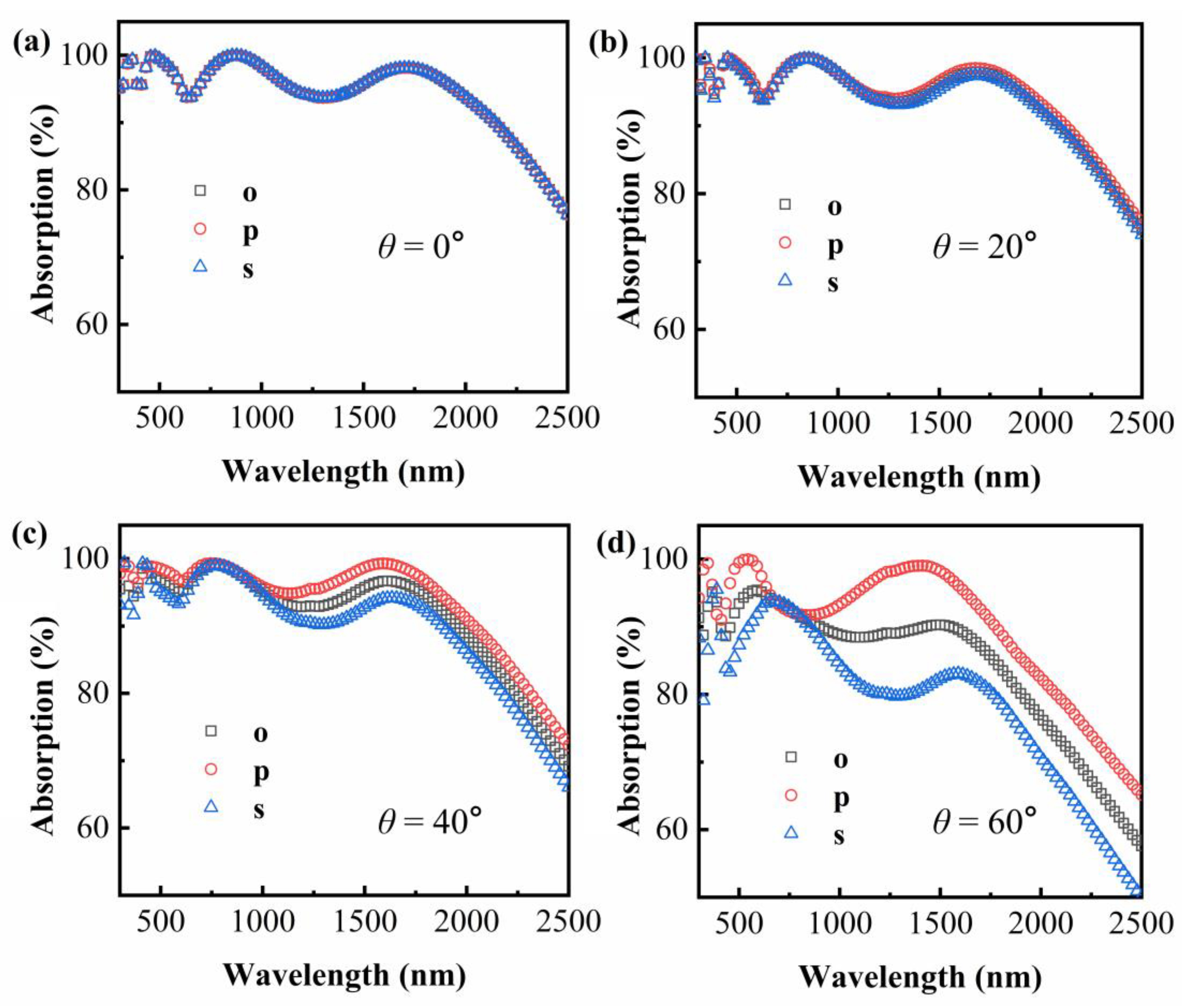
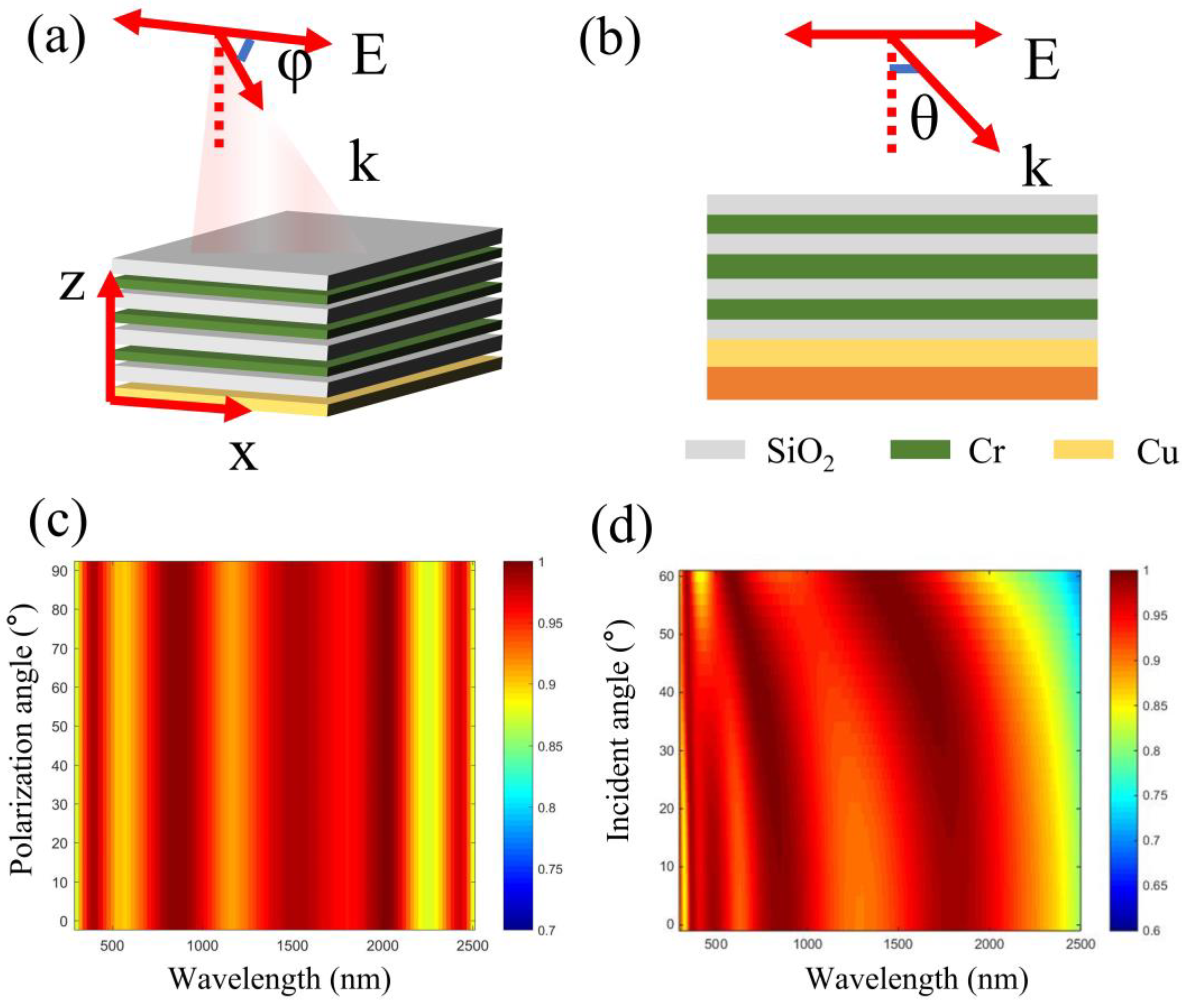
3.2. Effect of Polarization
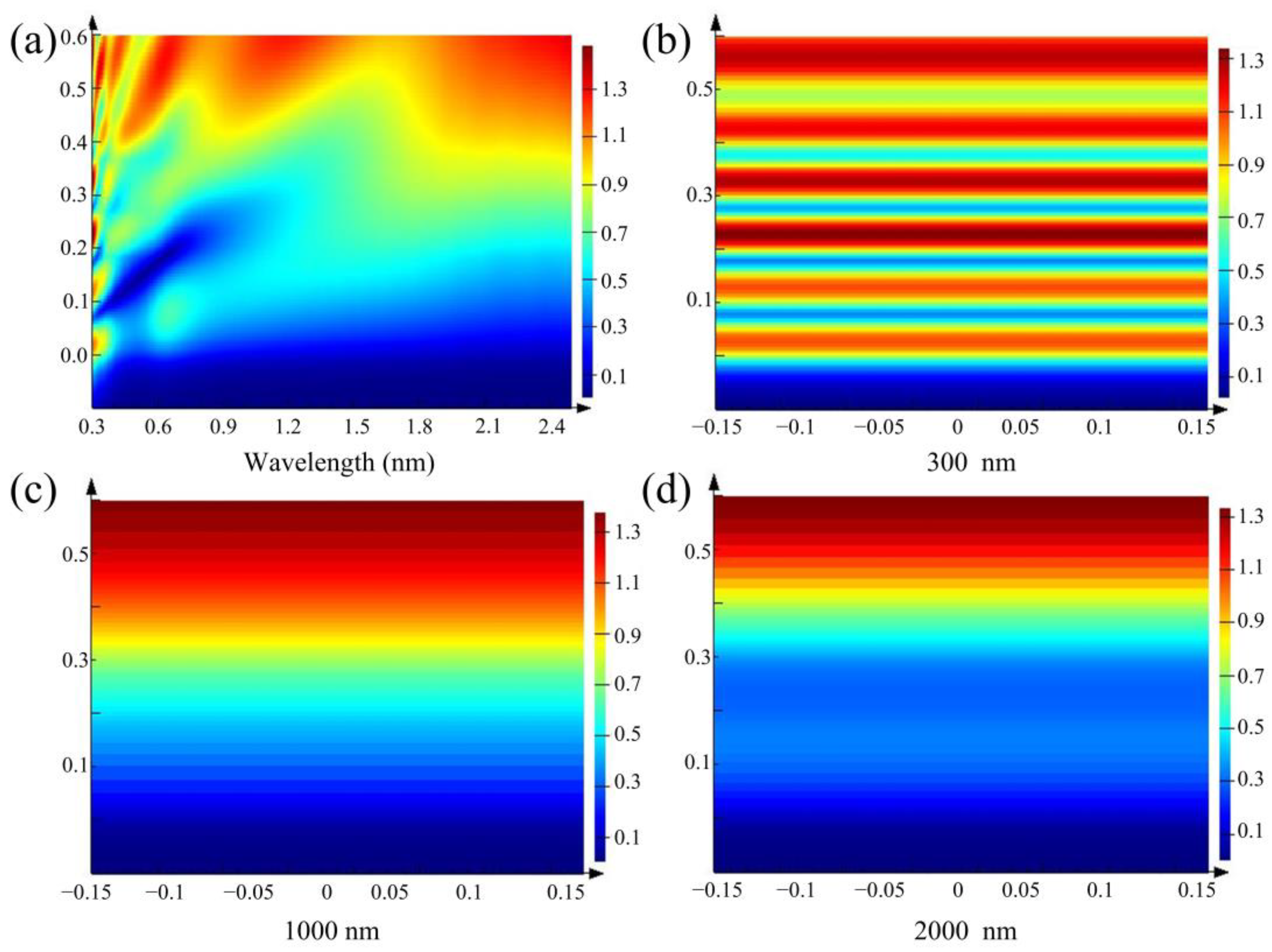
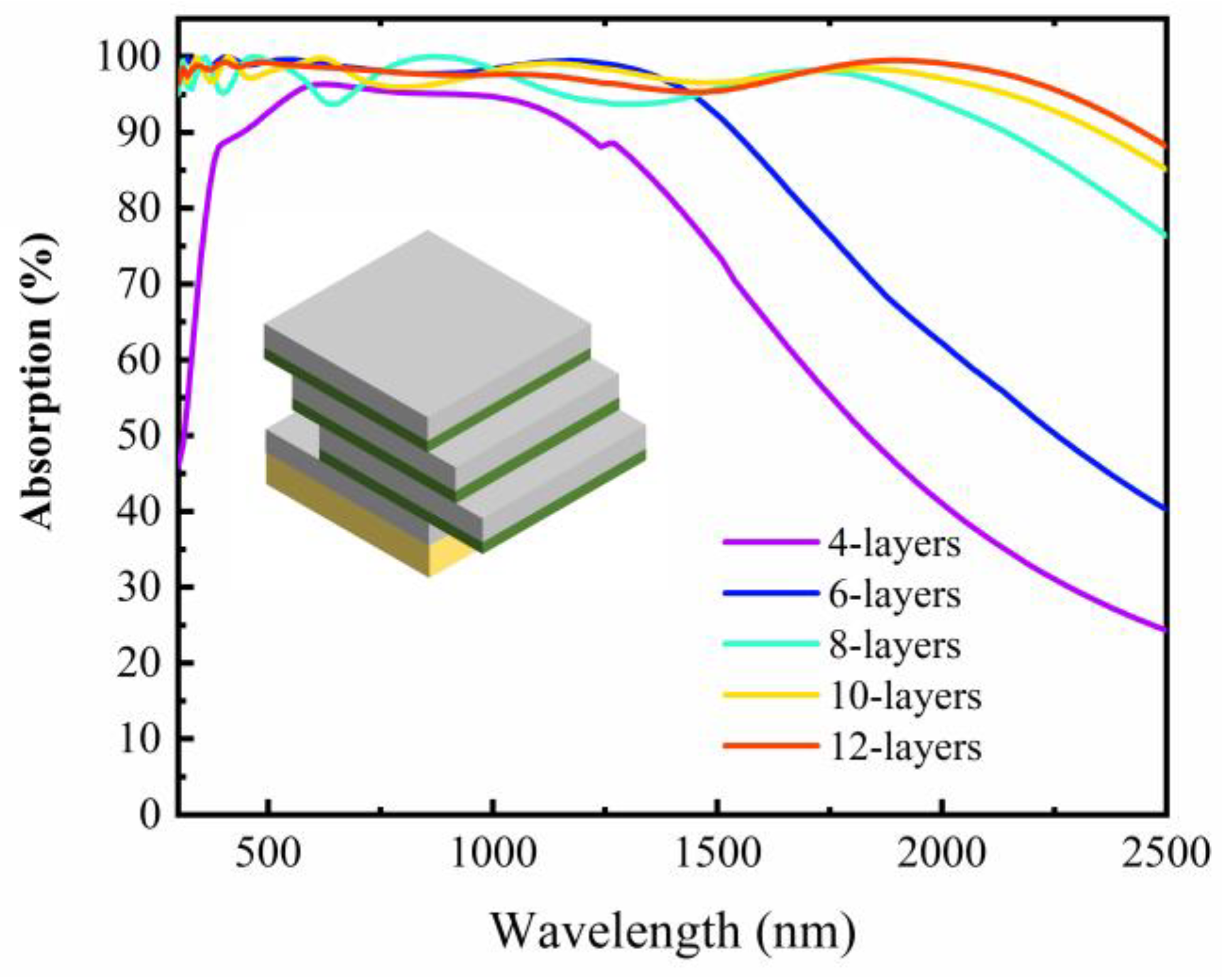
3.3. Effect of Layer Count
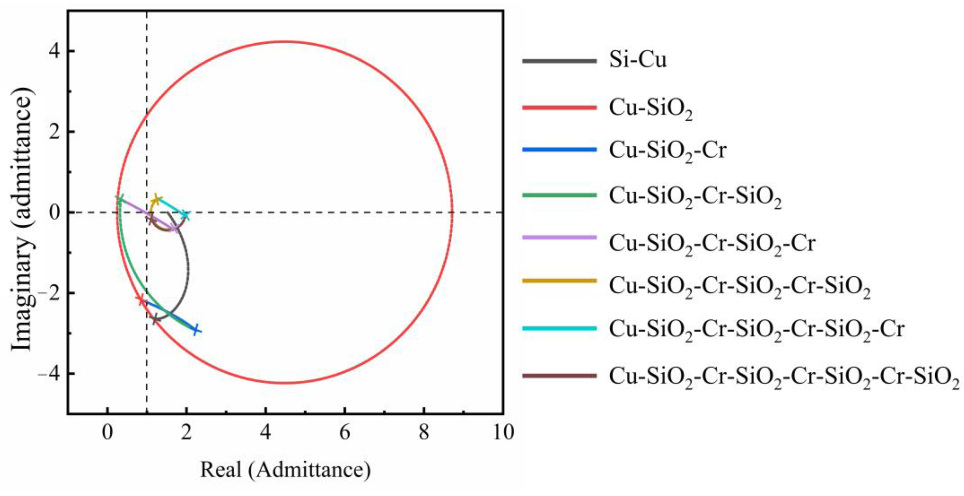
3.4. Admittance
3.5. Thermal Emissivity
4. Conclusions
Author Contributions
Funding
Data Availability Statement
Conflicts of Interest
References
- Kannan, N.; Vakeesan, D. Solar Energy for Future World: A Review. Renew. Sust. Energy Rev. 2016, 62, 1092–1105. [Google Scholar] [CrossRef]
- Lewis, N.S. Toward Cost-Effective Solar Energy Use. Science 2007, 315, 798–801. [Google Scholar] [CrossRef] [PubMed]
- Vo, T.T.E.; Ko, H.; Huh, J.-H.; Park, N. Overview of Solar Energy for Aquaculture: The Potential and Future Trends. Energies 2021, 14, 6923. [Google Scholar] [CrossRef]
- Kabir, E.; Kumar, P.; Kumar, S.; Adelodun, A.A.; Kim, K.-H. Solar Energy: Potential and Future Prospects. Renew. Sustain. Energy Rev. 2018, 81, 894–900. [Google Scholar] [CrossRef]
- Shah, A.; Torres, P.; Tscharner, R.; Wyrsch, N.; Keppner, H. Photovoltaic Technology: The Case for Thin-Film Solar Cells. Science 1999, 285, 692–698. [Google Scholar] [CrossRef] [PubMed]
- Weinstein, L.A.; Loomis, J.; Bhatia, B.; Bierman, D.M.; Wang, E.N.; Chen, G. Concentrating Solar Power. Chem. Rev. 2015, 115, 12797–12838. [Google Scholar] [CrossRef]
- Lin, Z.; Liu, H.; Qiao, T.; Hou, G.; Liu, H.; Xu, J.; Zhu, J.; Zhou, L. Tamm Plasmon Enabled Narrowband Thermal Emitter for Solar Thermophotovoltaics. Sol. Energy Mater. 2022, 238, 111589. [Google Scholar] [CrossRef]
- Zou, Y.; Zhang, C.; Yang, B.; Yi, Z.; Zhang, B.; Wu, X. Lithography-Free Solar Absorber Made of Multilayer w/SiO2 for Efficient Photothermal Conversion. Plasmonics 2023, 18, 1865–1871. [Google Scholar] [CrossRef]
- Cao, F.; McEnaney, K.; Chen, G.; Ren, Z. A Review of Cermet-Based Spectrally Selective Solar Absorbers. Energy Environ. Sci. 2014, 7, 1615–1627. [Google Scholar] [CrossRef]
- Xu, Z.; Zhang, L.; Zhao, L.; Li, B.; Bhatia, B.; Wang, C.; Wilke, K.L.; Song, Y.; Labban, O.; Lienhard, J.H.; et al. Ultrahigh-Efficiency Desalination via a Thermally-Localized Multistage Solar Still. Energy Environ. Sci. 2020, 13, 830–839. [Google Scholar] [CrossRef]
- Chen, C.; Zhou, L.; Yu, J.; Wang, Y.; Nie, S.; Zhu, S.; Zhu, J. Dual Functional Asymmetric Plasmonic Structures for Solar Water Purification and Pollution Detection. Nano Energy 2018, 51, 451–456. [Google Scholar] [CrossRef]
- Zhou, W.-X.; Shen, Y.; Hu, E.-T.; Zhao, Y.; Sheng, M.-Y.; Zheng, Y.-X.; Wang, S.-Y.; Lee, Y.-P.; Wang, C.-Z.; Lynch, D.W.; et al. Nano-Cr-Film-Based Solar Selective Absorber with High Photo-Thermal Conversion Efficiency and Good Thermal Stability. Opt. Express 2012, 20, 28953. [Google Scholar] [CrossRef] [PubMed]
- Yang, Y.-T.; Cai, Q.-Y.; Liu, D.-Q.; Gao, L.-S.; Zhang, H.-T.; Peng, L.; Hu, E.-T.; Liu, B.-J.; Luo, H.-H.; Zhang, R.-J.; et al. Low Polarization-Sensitive Ultra-Broadband Anti-Reflection Coatings with Improved Reliability. Opt. Express 2023, 31, 25477. [Google Scholar] [CrossRef]
- Ritchie, I.T.; Window, B. Applications of Thin Graded-Index Films to Solar Absorbers. Appl. Opt. 1977, 16, 1438. [Google Scholar] [CrossRef] [PubMed]
- Meng, Q.; Chen, F.; Cheng, S.; Xu, Y.; Yang, W.; Yi, Z. Near Perfect and Polarization Insensitive Broadband Absorber Based on Al2O3-Ti-Al2O3 Triple Layer Structure. Phys. Scr. 2023, 98, 025511. [Google Scholar] [CrossRef]
- Chen, B.; Shan, S.; Liu, J.; Zhou, Z. An Effective Design of Thermophotovoltaic Metamaterial Emitter for Medium-Temperature Solar Energy Storage Utilization. Sol. Energy 2022, 231, 194–202. [Google Scholar] [CrossRef]
- Yuan, H.; Yi, Y.; Song, Q.; Yi, Z.; Sun, T.; Tang, C.; Zeng, Q.; Cheng, S.; Wu, P. Ultra-Broadband Absorber and Perfect Thermal Emitter for High-Efficiency Solar Energy Absorption and Conversion. Renew. Energy 2024, 237, 121818. [Google Scholar] [CrossRef]
- Wang, Y.; Liu, Z.; Zhou, F.; Yi, Z.; Wang, J. Perfect Absorption Properties of a Near-Infrared Super-Surface Perfect Absorber Based on a Multilayer Subwavelength Array Structure. Phys. Lett. A 2025, 540, 130395. [Google Scholar] [CrossRef]
- Liu, Y.; Zhang, B.; Duan, J.; Xu, Y. Flexible Ultrawideband Microwave Metamaterial Absorber with Multiple Perfect Absorption Peaks Based on the Split Square Ring. Appl. Opt. 2018, 57, 10257–10263. [Google Scholar] [CrossRef]
- Xiong, H.; Hong, J.-S.; Luo, C.-M.; Zhong, L.-L. An Ultrathin and Broadband Metamaterial Absorber Using Multi-Layer Structures. J. Appl. Phys. 2013, 114, 064109. [Google Scholar] [CrossRef]
- Wu, B.; Liu, Z.; Liu, G.; Liu, X.; Tang, P.; Du, G.; Yuan, W.; Liu, M. An Ultra-Broadband, Polarization and Angle-Insensitive Metamaterial Light Absorber. J. Phys. D Appl. Phys. 2020, 53, 095106. [Google Scholar] [CrossRef]
- Li, X.-F.; Chen, Y.-R.; Miao, J.; Zhou, P.; Zheng, Y.-X.; Chen, L.-Y.; Lee, Y.-P. High Solar Absorption of a Multilayered Thin Film Structure. Opt. Express 2007, 15, 1907. [Google Scholar] [CrossRef] [PubMed]
- Liu, M.-H.; Hu, E.-T.; Yao, Y.; Zang, K.-Y.; He, N.; Li, J.; Zheng, Y.-X.; Wang, S.-Y.; Yoshie, O.; Lee, Y.; et al. High Efficiency of Photon-to-Heat Conversion with a 6-Layered Metal/Dielectric Film Structure in the 250–1200 Nm Wavelength Region. Opt. Express 2014, 22, A1843. [Google Scholar] [CrossRef]
- Zhang, Q.; Mills, D.R. Very Low-emittance Solar Selective Surfaces Using New Film Structures. J. Appl. Phys. 1992, 72, 3013–3021. [Google Scholar] [CrossRef]
- Sergeant, N.P.; Pincon, O.; Agrawal, M.; Peumans, P. Design of Wide-Angle Solar-Selective Absorbers Using Aperiodic Metal-Dielectric Stacks. Opt. Express 2009, 17, 22800–22812. [Google Scholar] [CrossRef]
- Kuang, K.; Wang, Q.; Yuan, X.; Yu, L.; Liang, Y.; Zhang, Y.; Peng, W. Ultra-Broadband Perfect Absorber Using Triple-Layer Nanofilm in a Long-Wave near-Infrared Regime. Appl. Opt. 2022, 61, 7706. [Google Scholar] [CrossRef] [PubMed]
- Ruud, C.J.; Cleri, A.; Maria, J.-P.; Giebink, N.C. Ultralow Index SiO2 Antireflection Coatings Produced via Magnetron Sputtering. Nano Lett. 2022, 22, 7358–7362. [Google Scholar] [CrossRef]
- Trotter, D.M.; Sievers, A.J. Spectral Selectivity of High-Temperature Solar Absorbers. Appl. Opt. 1980, 19, 711–728. [Google Scholar] [CrossRef]
- Xu, K.; Du, M.; Hao, L.; Mi, J.; Yu, Q.; Li, S. A Review of High-Temperature Selective Absorbing Coatings for Solar Thermal Applications. J. Mater. 2020, 6, 167–182. [Google Scholar] [CrossRef]
- Wang, Z.-Y.; Hu, E.-T.; Cai, Q.-Y.; Wang, J.; Tu, H.-T.; Yu, K.-H.; Chen, L.-Y.; Wei, W. Accurate Design of Solar Selective Absorber Based on Measured Optical Constants of Nano-Thin Cr Film. Coatings 2020, 10, 938. [Google Scholar] [CrossRef]
- Palik, E.D. Handbook of Optical Constants of Solids; Academic Press: Orlando, FL, USA, 1985; ISBN 0-12-544420-6. [Google Scholar]
- Yee, K. Numerical Solution of Initial Boundary Value Problems Involving Maxwell’s Equations in Isotropic Media. IEEE Trans. Antennas Propag. 1966, 14, 302–307. [Google Scholar] [CrossRef]


| Parameter | Material | Symbol | Quantity |
|---|---|---|---|
| Anti-reflection layer | SiO2 | h1 | 70.3 nm |
| Absorption layer | Cr | h2 | 2.3 nm |
| Transparent layer | SiO2 | h3 | 91.4 nm |
| Absorption layer | Cr | h4 | 4.4 nm |
| Transparent layer | SiO2 | h5 | 82.2 nm |
| Absorption layer | Cr | h6 | 7.2 nm |
| Transparent layer | SiO2 | h7 | 179.5 nm |
| Reflection layer | Cu | h8 | >100 nm |
| Layer Count | 4 | 6 | 8 | 10 | 12 |
|---|---|---|---|---|---|
| Average absorption | 69.77% | 82.3% | 94.26% | 96.5% | 97.07% |
| Angle | 0° | 10° | 20° | 30° | |
|---|---|---|---|---|---|
| Temperature | |||||
| 300 K | 0.20348 | 0.21603 | 0.21904 | 0.22405 | |
| 400 K | 0.20727 | 0.21468 | 0.21587 | 0.21785 | |
| 500 K | 0.22156 | 0.22602 | 0.22557 | 0.22487 | |
| 600 K | 0.2473 | 0.24988 | 0.24801 | 0.24495 | |
Disclaimer/Publisher’s Note: The statements, opinions and data contained in all publications are solely those of the individual author(s) and contributor(s) and not of MDPI and/or the editor(s). MDPI and/or the editor(s) disclaim responsibility for any injury to people or property resulting from any ideas, methods, instructions or products referred to in the content. |
© 2025 by the authors. Licensee MDPI, Basel, Switzerland. This article is an open access article distributed under the terms and conditions of the Creative Commons Attribution (CC BY) license (https://creativecommons.org/licenses/by/4.0/).
Share and Cite
Li, C.; Hu, E.-T.; Zheng, Y.-X.; Wang, S.-Y.; Yang, Y.-M.; Lee, Y.-P.; Guo, J.-P.; Cai, Q.-Y.; Duan, W.-B.; Chen, L.-Y. High-Efficiency Broadband Selective Photothermal Absorbers Based on Multilayer Chromium Films. Crystals 2025, 15, 562. https://doi.org/10.3390/cryst15060562
Li C, Hu E-T, Zheng Y-X, Wang S-Y, Yang Y-M, Lee Y-P, Guo J-P, Cai Q-Y, Duan W-B, Chen L-Y. High-Efficiency Broadband Selective Photothermal Absorbers Based on Multilayer Chromium Films. Crystals. 2025; 15(6):562. https://doi.org/10.3390/cryst15060562
Chicago/Turabian StyleLi, Chu, Er-Tao Hu, Yu-Xiang Zheng, Song-You Wang, Yue-Mei Yang, Young-Pak Lee, Jun-Peng Guo, Qing-Yuan Cai, Wei-Bo Duan, and Liang-Yao Chen. 2025. "High-Efficiency Broadband Selective Photothermal Absorbers Based on Multilayer Chromium Films" Crystals 15, no. 6: 562. https://doi.org/10.3390/cryst15060562
APA StyleLi, C., Hu, E.-T., Zheng, Y.-X., Wang, S.-Y., Yang, Y.-M., Lee, Y.-P., Guo, J.-P., Cai, Q.-Y., Duan, W.-B., & Chen, L.-Y. (2025). High-Efficiency Broadband Selective Photothermal Absorbers Based on Multilayer Chromium Films. Crystals, 15(6), 562. https://doi.org/10.3390/cryst15060562