Article

Optimizing the Morphology and Optical Properties of MoS2 Using Different Substrate Placement: Numerical Simulation and Experimental Verification

1
School of Physics and Electronic Information, Anhui Normal University, Wuhu 241003, China
2
Anhui Province Key Laboratory for Control and Applications of Optoelectronic Information Materials, Wuhu 241003, China
3
College of Physics, Guizhou University, Guiyang 550025, China
*
Authors to whom correspondence should be addressed.
Crystals 2025, 15(1), 59; https://doi.org/10.3390/cryst15010059
Submission received: 24 December 2024 / Revised: 5 January 2025 / Accepted: 7 January 2025 / Published: 8 January 2025

Abstract

:
The prerequisite for rapid and steady development of TMDC-based optoelectronic devices is high efficiency in materials preparation, which relies on a mature synthesis technique and optimized production conditions. Visualization based on numerical simulation, which illustrates the impact of growth parameters on deposited products, is helpful to understand formation mechanisms and modify growth conditions. In this work, we construct two models with two different substrate placements, where the substrate is parallel or perpendicular to gas flow direction. The simulation results show more velocity distribution uniformity across a wider range from −1.4 cm to 1.4 cm for vertically placed (VP) compared to horizontally placed (HP) substrates. The calculated average velocities of 0.048, 0.053, 0.078, 0.137, and 0.391 cm/s along five different positions on the VP substrate are greater than the values of 0.027, 0.026, 0.025, 0.023, and 0.036 cm/s on the HP substrate. Comparing the precursor concentration distributions on both substrates, it is observed that the S molar concentration gradient on both substrates is negligible and the uniform Mo molar concentrations from z = −1.4 cm to 2.0 cm on the VP substrate ensure minimal change in the S/Mo ratio, which contributes to forming single-morphology domains. Furthermore, increasing the distance between the precursor inlets and the VP substrate decreases the amount of molecules on the substrate surface, achieving near-stoichiometry and promoting monolayer deposition. This is verified by the experimental result, which showed gentle morphological transformation on the VP substrate from a truncated triangle to a hexagon, and then back to a truncated triangle. By contrast, the multi-morphology and thickness of MoS2 on the HP substrate result from the complex Mo concentration along the flow direction. Moreover, PL intensities of the MoS2 domains deposited on the VP substrate are enhanced by 11.9-fold compared to the average intensity on the HP substrate. This result indicates the MoS2 grown on the VP substrate has less intrinsic defects than that grown on the HP substrate. The combination of numerical simulation with experimental methods facilitates the visualization of invisible growth conditions, which provides effective guidance for using simulation results for other TMDC materials.

1. Introduction

Two-dimensional (2D) transition metal dichalcogenides (TMDCs) have become a hot research topic in the fields of optoelectronics [1,2], nonlinear photonics [3,4] and micro-cavity optics [5,6,7] in the past decades, which have been complimented by increasingly mature material preparation and integration technology. Among various preparation methods, chemical vapor deposition (CVD) [8,9,10], which is capable of fabricating high-quality TMDC materials with uniform thickness over a large area, has been widely used.
Previous studies have revealed that the growth behaviors of TMDC in a CVD process are closely correlated with growth temperature [11], substrate materials [12], and promoters [13,14], etc. In a typical growth [15], transition metal oxide powder is loaded into an alumina boat in the central heating zone of a tube furnace, and chalcogen powder is placed in the upstream zone, while the substrate is horizontally placed (HP) face down above the transition metal oxide or at the downstream side. High-purity argon gas carries the precursor horizontally through the substrate, forming a precursor concentration gradient along the gas flow direction, which coordinates with the temperature gradient, resulting in the growth of TMDC materials with different morphologies, sizes [16], and thicknesses on the same substrate.
Recently, several original schemes have been explored in experiments and simulations; some investigation factors and methods are listed in Table S1. Li et al. [9] achieved wafer-scale monolayer MoSe2 films with excellent uniformity on a vertically placed (VP) substrate by combining a multisource design. Johari et al. [11] simulated the effect of substrate orientations (0, 20, 45, 70, and 90°) and proved that non-uniformity gradually reduces with increasing substrate angles, reaching a minimum at 90°. There is no doubt that simulation results illustrate the distribution of invisible factors and provide guidance for subsequent experimental programs. On the other hand, achievable experimental results are essential to verify the feasibility of a developed model. Hence, Zhou et al. [17] firstly modified key parameters including precursor mixing, fluid velocity, and shear stress using computational fluid dynamics analysis and then obtained inch-scale monolayer MoSe2. Zhang et al. [18] improved material uniformity by changing the substrate placement from face down to face up, which was demonstrated using experimental and simulation methods. Obviously, substrate placement has a significant impact on the uniformity of the resultant TMDCs, which can be attributed to the distinct growing microenvironments (precursor concentrations) at different positions. The precursor is carried by the gas flow, and thus, the concentration distribution of the precursor is determined by the flow-field distribution. However, it is difficult to experimentally investigate flow field in a tube. Therefore, a detailed simulation of the growth environment is helpful to optimize growth conditions and provide a deeper understanding of the CVD process. Moreover, TMDC materials are usually applied to develop optic devices, like light-emitters, which require a high PL quantum yield. Hence, optical measurements are necessary to evaluate potential applications. Here, we construct two simplified models to calculate and compare the gas flow and concentration distributions on the surfaces of VP and HP substrates using the COMSOL Multiphysics® software package 5.5. A fluid-flow simulation is employed to derive flow-rate distributions in different cross-sections. Precursor concentration gradient computations help to reveal the growth microenvironment of the MoS2 domains. Finally, experiments are performed to compare the morphologies and PL emissions of the MoS2 domains on substrates with different placements. The results indicate that the monolayer MoS2 domains grown on the VP substrate exhibit a more uniform structure, fewer intrinsic defects, and thus, a better PL emission performance than those grown on the HP substrate, which is consistent with the simulation results.

2. Materials and Methods

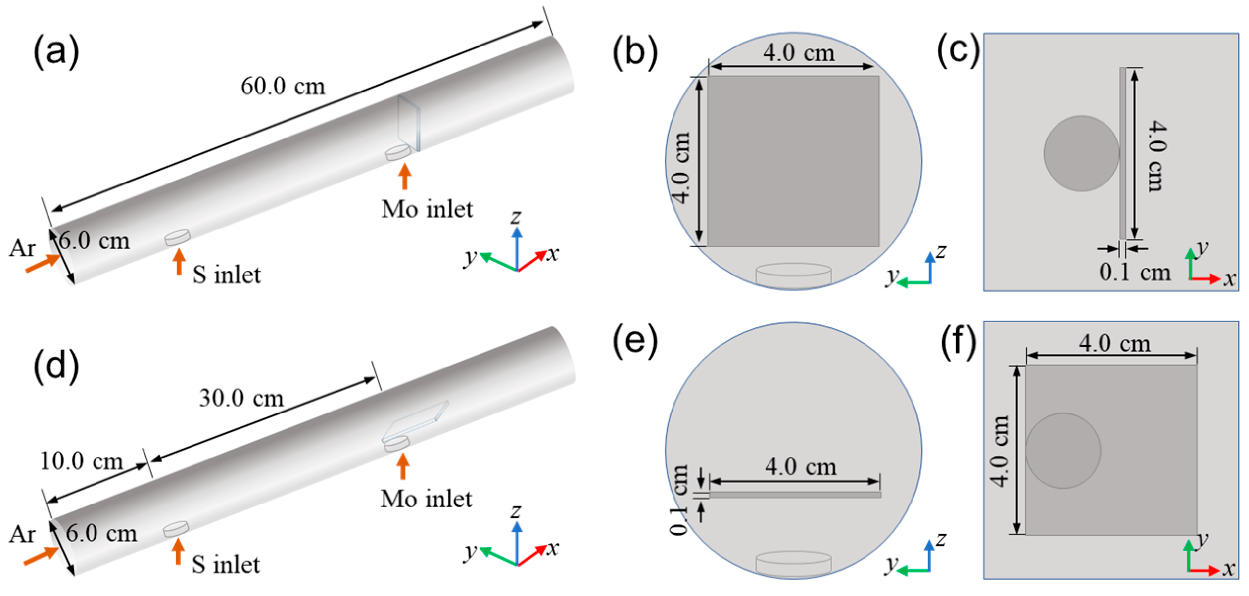
2.1. The Numerical Models

According to our experimental setup [6,19], two simplified 3D models consisting of a quartz tube (6.0 cm in diameter and 60.0 cm in length) and a quartz substrate (4.0 cm × 4.0 cm × 0.1 cm) were constructed, as shown in Figure 1a,d, where the substrate was placed vertically and parallel to the gas flow direction, respectively. The corresponding left view and top view are illustrated in Figure 1b,c,e,f. The gas phase sulfur (S) inlet was 30 cm away from the molybdenum (Mo) inlet, and 10 cm from the carrier gas inlet. In the simulations, a flow rate of 200 sccm was used for argon gas, and the molar concentrations of Mo and S were set to 0.002 and 0.09 mol/m3, respectively, which were obtained according to the reactant proportions used in experiment. Based on the experimental process, three modules, namely, fluid flow, structural mechanics and chemical species transport were combined in the simulation platform using COMSOL Multiphysics software 5.5.

2.2. Synthesis of MoS2

As reported in our previous work [6], a home-built CVD system equipped with a single-zone tubular furnace and a 6.0 cm diameter of quartz tube was used to synthesize the MoS2. As shown in Figure S1a, an alumina boat containing sulfur powder (5 mg, Alfa Aesar, Shanghai, China) was first placed at the center of the heating zone, which was 30 cm away from another alumina boat containing molybdenum oxide (MoO3) (0.5 mg, Sinopharm Chemical Reagent Co., Ltd., Nanjing, China), which was placed upstream to the edge of the furnace. One piece of substrate (Si substrate with a 300 nm-thick oxygen layer) was placed above the MoO3 boat, which was parallel to the gas flow direction. To ensure the vertical position of the gas flow direction, another substrate was installed on an L-shaped quartz mounting plate and aligned with the backend of the MoO3 boat, as shown in Figure S1b. Argon gas with a flow rate of 200 sccm was introduced into the quartz tube to remove residual air and adjust growth pressure. The furnace was heated to a temperature of 850 °C and then maintained for 5 min under atmospheric pressure. Following this, the temperature naturally cooled down to room temperature.

2.3. Optical Measurement of PL and Raman Spectra

A CW 532 nm excitation light (MSL-FN-532, Changchun New Industries Optoelectronics Technology Co., Ltd., Changchun, China) was used to excite the PL and Raman spectra of the MoS2 samples. The light beam was focused on the samples through a 50× objective (LU Plan, Nikon, Tokyo, Japan) with a diameter of 2 μm. Emissions were collected using the same 50× objective through a 532 nm notch filter (NF01-532U-25, Semrock, Rochester, NY, USA) and then split by a beam splitter between a spectrometer (iHR320, HORRIBA, Osaka, Japan) for spectral analysis and a CCD camera for imaging.

3. Results

3.1. The Simulation Results

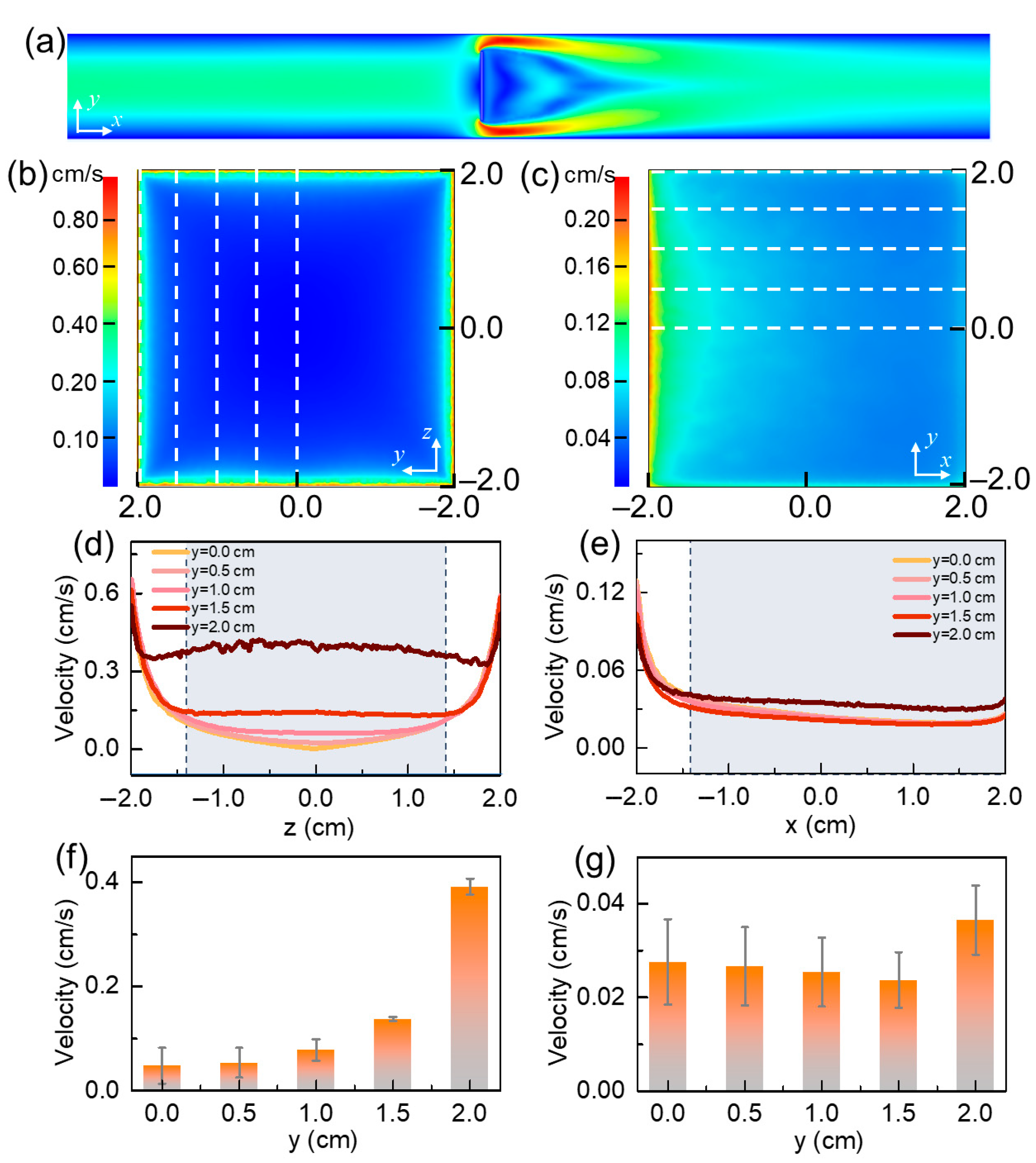
3.1.1. Velocity Distribution

During the CVD process, a thin fluid layer, namely, the boundary layer, that differs from the free stream, was found to exist near the substrate surface. The precursor concentration [18], flow velocity [17] and viscous force in the boundary layer had a great impact on the thickness and morphology of the resultant film. Among these factors, the velocity distribution is considered critical because it affects the crystal distribution by changing the deposition rate of the precursors. Therefore, we simulated the velocity field around the VP substrate and compared it with that of the HP substrate. The top view (x-y plane) of the velocity field around the VP substrate is shown in Figure 2a, in which high velocity occurs at the narrow gaps between the tube and substrate. Figure 2b presents the 2D velocity distribution (y-z plane) near the substrate surface; good uniformity can clearly be observed. The velocity is symmetric around the y = 0 axis due to the structural symmetry. The velocity values at varying heights (z) corresponding to five different horizontal locations (y = 0.0, 0.5, 1.0, 1.5, and 2.0 cm) are plotted in Figure 2d. These velocity curves exhibit two distinct features. One is that the velocity changes rapidly around the edge regions of the substrate, which is attributed to the singularity at the substrate edges [11] that influences the transport processes. The other is that the velocity slightly changes in the wider central region, ranging from z = −1.4 cm to 1.4 cm, which is the proper region for uniform deposition. In comparison, different behavior was observed on the HP substrate (Figure 2c), where the velocity rapidly decreased from the front edge of the substrate (x = −2.0 cm) to x = −1.4 cm, followed by a slow decrease toward the back edge, as shown in Figure 2e. The calculated average velocity crossing the uniform region is 0.048, 0.053, 0.078, 0.137, and 0.391 cm/s along y = 0.0, 0.5, 1.0, 1.5, 2.0 cm, respectively, on the VP substrate (Figure 2f), which is larger than the corresponding values (0.027, 0.026, 0.025, 0.023, and 0.036 cm/s) on the HP substrate (Figure 2g). A previous study [18] has defined boundary layer thickness (δ) using Equation (1):
δ ( h ) = 5 h Re ( h )
where h is the distance from the substrate surface, Re(h) is the Reynolds number, which can be roughly expressed as Re(h)∝v0, and v0 is the flow velocity. Obviously, the thickness of the boundary layer (δ) reduces with increasing fluid velocity, and reactant molecules are more easily absorbed on a thinner boundary layer. For the HP substrate, a constant distance (h) is maintained while velocity rapidly decreases from the front edge of the substrate, followed by a slow decrease toward the back edge. According to Equation (1), gradually varied and small velocities lead to a non-uniform thick boundary layer. This is different from the VP substrate, where larger velocities in a uniform distribution result in a thin boundary layer, promoting the epitaxy growth process of domains on the substrate. Furthermore, subsequent simulation results show that the distance between the S or Mo inlet and the substrate is another important factor determining precursor concentration.

3.1.2. Precursor Molar Concentration

It is well known that the size and morphology [20,21] of TMDCs are related to precursor concentration at the deposition site. In a typical experimental setup, the distribution of chalcogens on the substrate can be considered uniform because the chalcogen inlet is far from the substrate. However, the substrate is near the transition metal inlet, resulting in an obvious difference in transition metal concentration at different positions on the substrate. Therefore, the deposited pattern is greatly affected by the concentration gradient of the transition metals on the substrate. Figure 3a presents the simulated concentration distributions of S and Mo atoms on the VP substrate, which shows that the distribution of S atoms is more uniform than Mo atoms. The molar concentrations of S and Mo along five different horizontal positions (y = 0.0, 0.5, 1.0, 1.5, 2.0 cm) are plotted in Figure 3c. The data show that the S molar concentrations are about 6.0 × 10⁻⁴ ± 4.8 × 10⁻⁴ mol/m3 across the entire wafer, while the Mo molar concentrations gradually decrease and then flatten out with increasing height. Correspondingly, the S/Mo ratio changes along the z direction, resulting in the morphological transformation of MoS2 at different heights, which will be further discussed in the following experimental section. As a comparison, the simulated concentration distributions of S and Mo atoms on the HP substrate are presented in Figure 3b, d. The molar concentration of S atoms is in the range of 2.0 × 10⁻³ ± 6.9 × 10⁻⁴ mol/m3—such a small concentration gradient is negligible [22,23]—and the S molar concentration is considered constant. However, there is a significant difference in Mo atom concentration on the substrate: the closer the substrate to the reactant inlet, the higher the Mo molar concentration. The corresponding concentration curves shown in Figure 3d further reveal that the molar concentration of Mo atoms first increases, then decreases, and finally flattens. Such a complex concentration distribution on the HP substrate will lead to the deposition of MoS2 with multiple morphologies. The possible deposition regions for monolayer MoS2 films are in the downstream region and at the side edges of the substrate, while multi-layer films should occur in the upstream region due to excessive Mo atoms, which lead to the formation of numerous nucleation sites.

3.2. The Morphology of MoS2 Deposited on SiO2/Si Substrate
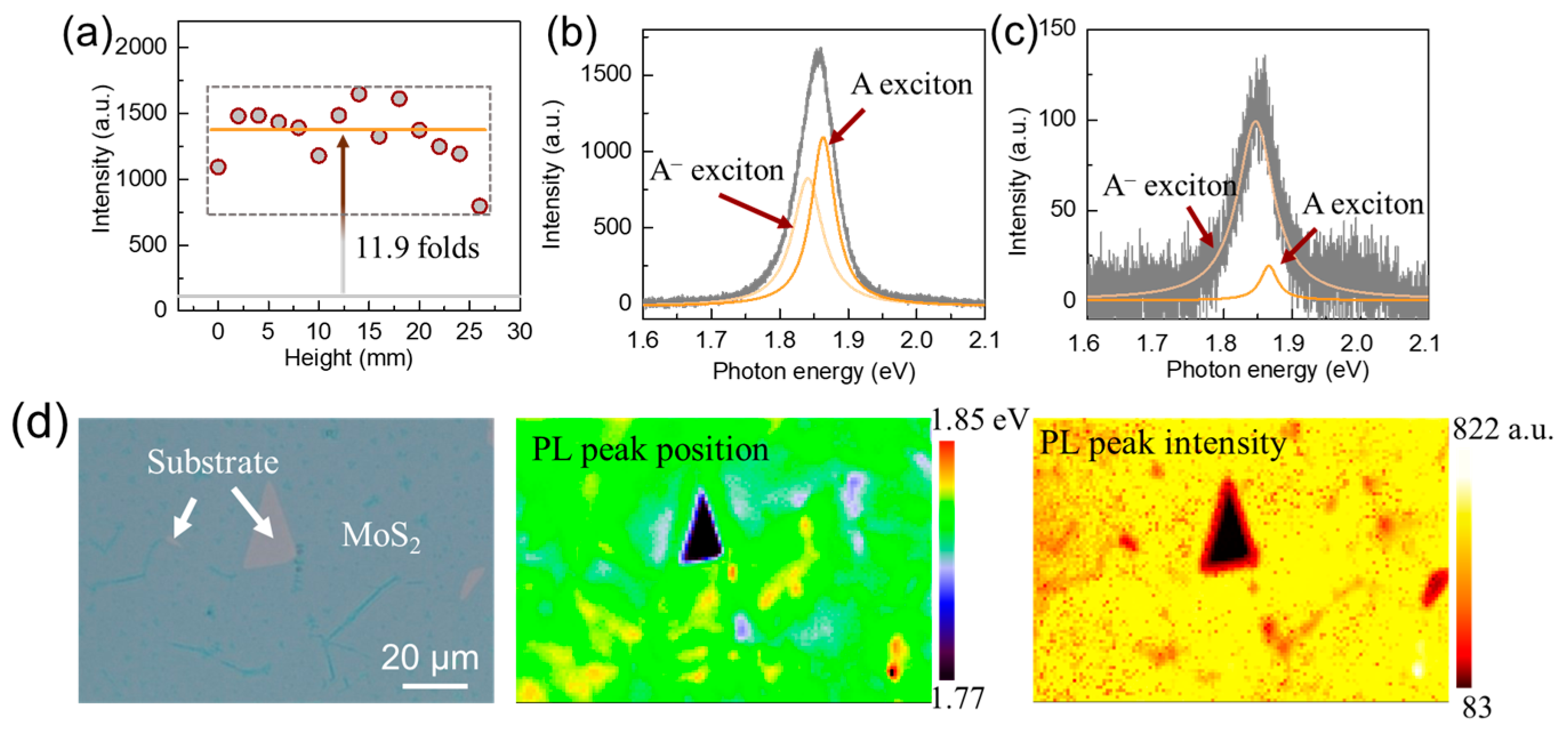
To verify the simulated results, comparative experiments with two different substrate placements were separately performed. Figure 4a,b shows the single-deposition pattern of MoS2 on the VP and HP substrate, respectively. The indistinctive color contrast of the VP substrate indicates uniform precursor molecules on the full substrate [9], which is consistent with the simulation result in Figure 3a. On the substrate, the S atom concentration gradient can be ignored due to the long distance between the S source and the substrate, while the Mo atom concentration varies gently at a height range from z = −1.4 cm to 2.0 cm, resulting in a small change in the S/Mo atom ratio at different heights. Correspondingly, the deposited MoS2 domains experience a morphological transformation from a truncated triangle (position I) to a hexagon (position II), then back to a truncated triangle (position III), as shown in Figure 4c. Such a morphological transformation can be explained by the hexagonal qualitative model reported previously [16], which consists of three sides of Mo-zigzag (Mo-zz) terminations and another three sides of S-zigzag (S-zz) terminations. At position I, close to the Mo source which has a low S/Mo atom ratio, the probability of the S-zz terminations meeting and bonding with Mo atoms is higher than that of the Mo-zz terminations bonding with S atoms; thus, truncated triangle domains are preferential because of the faster growth rate of the S-zz terminations than Mo-zz terminations. At a higher position (position II), the probabilities of the two types of terminations bonding with their corresponding free atoms are similar, eventually leading to the formation of hexagonal domains. As the height increases to position III, the Mo concentration further decreases, so that the growth rate of Mo-zz terminations is faster than S-zz terminations, and the shape of MoS2 returns to a truncated triangle. Such a gentle morphological transformation indicates that the S/Mo ratio approaches near stoichiometry. On the contrary, multiple morphologies of MoS2 are observed at different positions on the HP substrate, as shown in Figure 4d. This observation reflects a different concentration distribution of Mo atoms along the gas flow direction. Comparing the SEM images in Figure S2a, multi-layer MoS2 (light white areas in position ⅰ–ⅲ) was deposited on the upstream region closer to the Mo source, where the proportion of Mo atoms is quite high. This observation aligns with the Mo molar concentration curves in the simulation. Further, the AFM image in Figure S2b characterizes the monolayer nature of the deposited domains, which occur in the downstream region (position iv), where low concentrations of both S and Mo decrease the nucleation sites and promote epitaxial growth, while a triangular shape indicates that the S/Mo ratio is far above stoichiometry.

3.3. PL Emissions

PL emission [24,25,26,27] is an important indicator used to assess the quality of MoS2 materials. In general, mismatched stoichiometry leads to the formation of intrinsic defects [28] including vacancies [29], impurities [30] and grain boundaries in TMDCs, which increases the nonradiative recombination pathway, thereby weakening the PL intensity. Figure 5a shows the PL intensities of the MoS2 domains deposited on the VP substrate. The calculated average intensity is 1404.0 a. u. (yellow line), which is enhanced by a factor of 11.9 compared to the average intensity (118.1 a. u., gray line) on the HP substrate. This result indicates that the MoS2 grown on the VP substrate is near stoichiometric and has fewer intrinsic defects than that grown on the HP substrate. Moreover, excess electrons originated from defect-induced doping are prone to bind with photoexcited electron-hole pairs. The recombination of such charged excitons generates an A exciton feature in the PL spectrum. It is observed that the A exciton emission is dominant in the PL spectrum of the MoS2 deposited on the HP substrate (Figure 5c). However, for the MoS2 grown on the VP substrate, the A exciton is significantly inhibited, and the A exciton dominates the emission (Figure 5b), which is expected to achieve a high quantum yield. Furthermore, there are no shifts for the Raman modes located at 384 cm−1 (E2g mode) and 402 cm−1 (A1g mode), which are extracted from the Raman spectra of MoS2 at different heights of the VP substrate, as shown in Figure S3, again revealing their similar atomic arrangement. The maps showing PL peak position and intensity for MoS2 on the VP substrate, illustrated in Figure 5d, clearly show its good uniformity, indicating its great potential for application in TMDC-based light-emitting devices.

4. Discussion

The simulation visualizes the growth parameters during the deposition process and optimizes growth conditions. The experimental results strongly support the simulation’s feasibility. In this work, two simulation models, in which the substrate was vertical and horizontal to the gas flow direction, were constructed to compare their velocity and precursor concentration distribution, which determined the morphology and thickness of MoS2. The uniform velocity distribution on the VP substrate indicates the potential region for monolayer domain deposition. The S molar concentration gradient for both substrate placements is negligible, while the concentration of Mo located closer to the substrate would determine the precursor ratio in different locations and affect the growth procedure. The observed morphological transformation from truncated triangles to hexagons, and then back to truncated triangles, reveals that the S/Mo ratios are approximately equal to 2.0, which is a suitable proportion for reactants, making it possible to grow ideal MoS2 domains containing fewer defects. This is confirmed in terms of optical characteristics, and the PL intensity of MoS2 on the VP substrate is 11.9 times higher than that on the HP substrate. The deconvolution of the PL spectrum shows that the weight of A exciton decreased due to the substrate placement change from horizontal to vertical. In summary, the following investigations were carried out: (1) a comparison of velocity and precursor distributions based on two numerical simulations where substrates were vertical and horizontal to gas flow direction; (2) an analysis of the relationship between MoS2 morphology and the simulated factors; (3) a 11.9-fold enhancement in PL intensity, indicating fewer intrinsic defects of MoS2 on the VP compared to the HP substrate. This work provides information to enhance the design and optimization of experiments using a simulation platform before material preparation, which can also be applied to synthesizing other TMDC materials using the CVD method. Although the approximate results are demonstrated using simplified models, there is some deviation originating from the original state of S and Mo and the related reaction kinetics. In future work, we will correct the simulation conditions to more closely align with the actual experiment and broaden the study candidates to TMDC heterostructures.

Supplementary Materials

The following supporting information can be downloaded at: https://www.mdpi.com/article/10.3390/cryst15010059/s1, Figure S1. (a) The schematic for growing MoS2 by the CVD method, inset: horizontally placed (HP) substrate above MoO3 powder; (b) Vertically placed (VP) substrate aligned to the backend of the MoO3 boat; Figure S2. (a) The SEM images of MoS2 along flow direction; (b) the AFM image of monolayer MoS2 and corresponding height profile; Figure S3. Raman spectra of MoS2 on VP substrate; Table S1. Comparison of investigation factors and methods.

Author Contributions

Conceptualization, F.L.; methodology, F.L. and Y.Z.; software, F.L., Y.Z., Y.Y. and Q.X.; validation, F.L. and Z.Z.; formal analysis, F.L.; investigation, Z.Z.; resources, F.L., S.L. and Q.X.; data curation, F.L.; writing—original draft preparation, F.L.; writing—review and editing, Z.Z.; visualization, F.L.; supervision, F.L. and Z.Z.; project administration, F.L. and Z.Z.; funding acquisition, F.L., Z.Z. and L.L. All authors have read and agreed to the published version of the manuscript.

Funding

This research was funded by National Natural Science Foundation of China, grant number 12104014, 12304333, 62341401, Anhui Province Natural Science Foundation, grant number 2108085QA28, 2008085QA35, University Annual Scientific Research Plan of Anhui Province, grant number 2023AH040029, and Guizhou Provincial Basic Research Program, grant number ZK[2024]071.

Data Availability Statement

The original contributions presented in this study are included in the article/Supplementary Material. Further inquiries can be directed to the corresponding authors.

Conflicts of Interest

The authors declare no conflicts of interest.

References

  1. Guo, B.; Xiao, Q.L.; Wang, S.H.; Zhang, H. 2D Layered Materials: Synthesis, Nonlinear Optical Properties, and Device Applications. Laser Photonics Rev. 2019, 13, 1800327. [Google Scholar] [CrossRef]
  2. Kumar, A.; Kumar, M. Recent Progress in Emerging 2D Transition-Metal Dichalcogenide-Based Gas Sensors: A Review. IEEE Sens. J. 2024, 24, 25221–25226. [Google Scholar] [CrossRef]
  3. Liu, X.F.; Guo, Q.B.; Qiu, J.R. Emerging Low-Dimensional Materials for Nonlinear Optics and Ultrafast Photonics. Adv. Mater. 2017, 29, 1605886. [Google Scholar] [CrossRef]
  4. Liao, F.; Wang, Y.; Peng, T.; Peng, J.; Gu, Z.Q.; Yu, H.K.; Chen, T.; Yu, J.X.; Gu, F.X. Highly Efficient Nonlinear Optical Conversion in Waveguiding GaSe Nanoribbons with Pump Pulses Down to a Femto-Joule Level. Adv. Opt. Mater. 2018, 6, 1701012. [Google Scholar] [CrossRef]
  5. Yu, J.X.; Xing, S.; Dai, G.Y.; Linghu, S.Y.; Gu, F.X. Direct-Bandgap Bilayer WSe2/Microsphere Monolithic Cavity for Low-Threshold Lasing. Adv. Mater. 2021, 34, 2106502. [Google Scholar] [CrossRef] [PubMed]
  6. Liao, F.; Yu, J.X.; Gu, Z.Q.; Yang, Z.Y.; Hasan, T.; Linghu, S.Y.; Peng, J.; Fang, W.; Zhuang, S.L.; Gu, M.; et al. Enhancing Monolayer Photoluminescence on Optical Micro/nanofibers for Low-threshold Lasing. Sci. Adv. 2019, 5, eaax7398. [Google Scholar] [CrossRef]
  7. Yu, J.X.; Yang, L.Q.; Gu, F.X. Metal Substrate Modulation for Realizing a More Compact Whispering-gallery Microcavity. Appl. Phys. Express 2021, 14, 064001. [Google Scholar] [CrossRef]
  8. Gong, Y.J.; Ye, G.L.; Lei, S.D.; Shi, G.; He, Y.M.; Lin, J.H.; Zhang, X.; Vajtai, R.; Pantelides, S.T.; Zhou, W.; et al. Synthesis of Millimeter-Scale Transition Metal Dichalcogenides Single Crystals. Adv. Funct. Mater. 2016, 26, 2009–2015. [Google Scholar] [CrossRef]
  9. Li, J.W.; Wang, S.P.; Li, L.; Wei, Z.; Wang, Q.Q.; Sun, H.C.; Tian, J.P.; Guo, Y.T.; Liu, J.Y.; Yu, H.; et al. Chemical Vapor Deposition of 4 Inch Wafer-Scale Monolayer MoSe2. Small Sci. 2022, 2, 2200062. [Google Scholar] [CrossRef]
  10. Sergeyev, D.; Duisenova, A.; Shunkeyev, K. Electronic and Optical Properties of One-Dimensional Van Der Waals Nanodevices Based on MoS2(n,n) and MoSe2(n,n) Nanotubes. Crystals 2024, 14, 1055. [Google Scholar] [CrossRef]
  11. Johari, M.H.; Sirat, M.S.; Mohamed, M.A.; Mustaffa, A.F.; Mohmad, A.R. Computational Fluid Dynamics In -sights into Chemical Vapor Deposition of Homogeneous MoS2 Film with Solid Precursors. Cryst. Res. Technol. 2023, 58, 2300139. [Google Scholar] [CrossRef]
  12. Zhou, D.; Shu, H.B.; Hu, C.L.; Jiang, L.; Liang, P.; Chen, X.S. Unveiling the Growth Mechanism of MoS2 with Chemical Vapor Deposition: From Two-Dimensional Planar Nucleation to Self-Seeding Nucleation. Cryst. Growth Des. 2018, 18, 1012–1019. [Google Scholar] [CrossRef]
  13. Kim, T.S.; Dhakal, K.P.; Park, E.; Noh, G.; Chai, H.J.; Kim, Y.; Oh, S.; Kang, M.; Park, J.; Kim, J.; et al. Gas-Phase Alkali Metal-Assisted MOCVD Growth of 2D Transition Metal Dichalcogenides for Large-Scale Precise Nucleation Control. Small 2022, 18, 2106368. [Google Scholar] [CrossRef]
  14. Zhu, L.J.; Yang, P.F.; Huan, Y.H.; Pan, S.Y.; Zhang, Z.Q.; Cui, F.F.; Shi, Y.P.; Jiang, S.L.; Xie, C.Y.; Hong, M.; et al. Scalable Salt-templated Directed Synthesis of High-Quality MoS2 Nanosheets Powders towards Energetic and Environmental Applications. Nano Res. 2020, 13, 3098–3104. [Google Scholar] [CrossRef]
  15. Zhou, J.D.; Lin, J.H.; Huang, X.W.; Zhou, Y.; Chen, Y.; Xia, J.; Wang, H.; Xie, Y.; Yu, H.M.; Lei, J.C.; et al. A Library of Atomically Thin Metal Chalcogenides. Nature 2018, 556, 355–359. [Google Scholar] [CrossRef]
  16. Wang, S.S.; Rong, Y.M.; Fan, Y.; Pacios, M.; Bhaskaran, H.; He, K.; Warner, J.H. Shape Evolution of Monolayer MoS2 Crystals Grown by Chemical Vapor Deposition. Chem. Mater. 2014, 26, 6371–6379. [Google Scholar] [CrossRef]
  17. Zhou, D.; Lang, J.; Yoo, N.; Unocic, R.R.; Wu, Q.H.; Li, B. Fluid-Guided CVD Growth for Large-Scale Monolayer Two-Dimensional Materials. ACS Appl. Mater. Interfaces 2020, 12, 26342–26349. [Google Scholar] [CrossRef]
  18. Zhang, F.; Wang, Z.P.; Zheng, K.; Feng, C.N.; Yao, R.; Tao, L.Q.; Yu, J.B.; Chen, X.P. Promoting Crystal Distribution Uniformity Based on the CVD Method with the Aid of Finite Element Methods. Cryst. Growth Des. 2020, 20, 777–782. [Google Scholar] [CrossRef]
  19. Shivayogimath, A.; Thomsen, J.D.; Mackenzie, D.M.A.; Geisler, M.; Stan, R.M.; Holt, A.J.; Bianchi, M.; Crovetto, A.; Whelan, P.R.; Carvalho, A.; et al. A Universal Approach for the Synthesis of Two-dimensional Binary Compounds. Nat. Commun. 2019, 10, 2957. [Google Scholar] [CrossRef]
  20. Buchkov, K.; Rafailov, P.; Minev, N.; Videva, V.; Strijkova, V.; Lukanov, T.; Dimitrov, D.; Marinova, V. Meta tungstate Chemical Vapor Deposition of WSe2: Substrate Effects, Shapes, and Morphologies. Crystals 2024, 14, 184. [Google Scholar] [CrossRef]
  21. Cho, Y.J.; Sim, Y.; Lee, J.H.; Hoang, N.T.; Seong, M.J. Size and Shape control of CVD-grown monolayer MoS2. Curr. Appl. Phys. 2023, 45, 99–104. [Google Scholar] [CrossRef]
  22. Loginov, A.B.; Kuvatov, M.M.; Ismagilov, R.R.; Sapkov, I.V.; Fedotov, P.V.; Kleshch, V.I.; Obraztsova, E.D.; Obraztsov, A.N. Evolution of Transition Metal Dichalcogenide Film Properties during Chemical Vapor Deposition: From Monolayer Islands to Nanowalls. Nanotechnology 2024, 35, 415601. [Google Scholar] [CrossRef]
  23. Liao, F.; Huang, H.D.; Xie, Q.Q.; Zeng, Y.H.; Liang, L.; Gu, F.X.; Zuo, Z.W. Broadband Tunable Resonance Modes from Multi-composition Monolayer MoS2(1−x)Se2x with SiO2 Microsphere Cavity. Appl. Phys. Lett. 2024, 124, 243103. [Google Scholar] [CrossRef]
  24. Politano, G.G.; Versace, C. Recent Advances in the Raman Investigation of Structural and Optical Properties of Graphene and Other Two-Dimensional Materials. Crystals 2023, 13, 1357. [Google Scholar] [CrossRef]
  25. Carozo, V.; Wang, Y.X.; Fujisawa, K.; Carvalho, B.R.; Mccreary, A.; Feng, S.M.; Lin, Z.; Zhou, C.J.; Perea-Lopez, N.; Elias, A.L.; et al. Optical Identification of Sulfur Vacancies: Bound Excitons at the Edges of Monolayer Tungsten Disulfide. Sci. Adv. 2017, 3, e1602813. [Google Scholar] [CrossRef] [PubMed]
  26. Mouri, S.; Miyauchi, Y.; Matsuda, K. Tunable Photoluminescence of Monolayer MoS2 via Chemical Doping. Nano Lett. 2013, 13, 5944–5948. [Google Scholar] [CrossRef]
  27. Ross, J.S.; Wu, S.F.; Yu, H.Y.; Ghimire, N.J.; Jones, A.M.; Aivazian, G.; Yan, J.Q.; Mandrus, D.G.; Xiao, D.; Yao, W.; et al. Electrical Control of Neutral and Charged Excitons in a Monolayer Semiconductor. Nat. Commun. 2013, 4, 1474. [Google Scholar] [CrossRef]
  28. Zheng, Y.J.; Chen, Y.F.; Huang, Y.L.; Gogoi, P.K.; Li, M.Y.; Li, L.J.; Trevisanutto, P.E.; Wang, Q.X.; Pennycook, S.J.; Wee, A.T.S.; et al. Point Defects and Localized Excitons in 2D WSe2. ACS Nano 2019, 13, 6050–6059. [Google Scholar] [CrossRef]
  29. Zhou, M.F.; Wang, W.H.; Lu, J.P.; Ni, Z.H. How Defects Influence the Photoluminescence of TMDCs. Nano Res. 2021, 14, 29–39. [Google Scholar] [CrossRef]
  30. Komsa, H.P.; Kurasch, S.; Lehtinen, O.; Kaiser, U.; Krasheninnikov, A.V. From Point to Extended Defects in Two-dimensional MoS2: Evolution of Atomic Structure under Electron Irradiation. Phys. Rev. B 2013, 88, 035301. [Google Scholar] [CrossRef]
Figure 1. (a) Schematic diagram of 3D CVD model for VP and (d) HP substrate in simulation; (b) The corresponding left view and (c) top view for VP substrate; (e) The corresponding left view and (f) top view for HP substrate.
Crystals 15 00059 g001
Figure 2. (a) Velocity contour in the top view (x-y plane) of the VP substrate; velocity distribution near the surface of VP (b) and HP (c) substrate; (d) velocities and (f) average velocities crossing the uniform region at varying heights corresponding to five different horizontal locations (y = 0.0, 0.5, 1.0, 1.5, and 2.0 cm) on the VP substrate; (e) velocities for HP substrate along five lines and their average values (g).
Crystals 15 00059 g002
Figure 3. (a) Mo and S concentration distributions near the VP and (b) HP substrate; (c,d) molar concentrations of S and Mo along five different locations indicated in (a,b).
Crystals 15 00059 g003
Figure 4. (a) The single deposition pattern of MoS2 on VP and HP substrates (SiO2/Si) (b); (c,d) the optical images at different locations indicated in (a,b), respectively.
Crystals 15 00059 g004
Figure 5. (a) PL intensity values of MoS2 domains deposited at different heights on VP substrate. The yellow and gray lines represent the average PL intensity on VP and HP substrate, respectively; (b,c) PL spectrum and its deconvolution of MoS2 on (b) VP and (c) HP substrate. The light and deep yellow curves represent A and A exciton, respectively; (d) optical image of large size MoS2 on VP substrate and its PL peak position and intensity map.
Crystals 15 00059 g005
Disclaimer/Publisher’s Note: The statements, opinions and data contained in all publications are solely those of the individual author(s) and contributor(s) and not of MDPI and/or the editor(s). MDPI and/or the editor(s) disclaim responsibility for any injury to people or property resulting from any ideas, methods, instructions or products referred to in the content.

