
Machinability of MoS2 after Oxygen Plasma Treatment under Mechanical Scanning Probe Lithography


Abstract
1. Introduction
2. Materials and Methods
2.1. Oxygen Plasma Treatment
2.2. Mechanical Scanning Probe Lithography
3. Results and Discussion
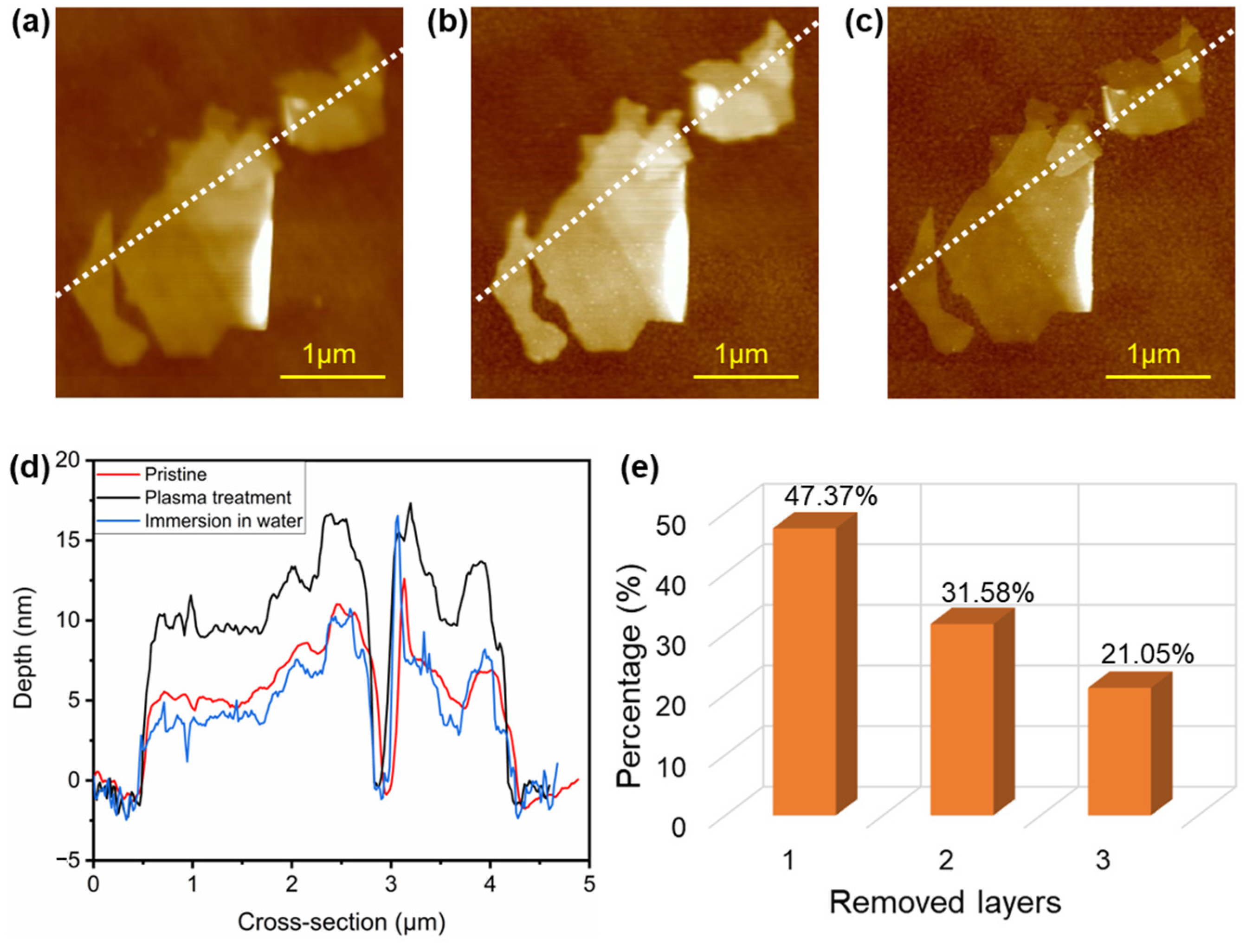
3.1. MoS2 Nanosheets under Oxygen Plasma Treatment
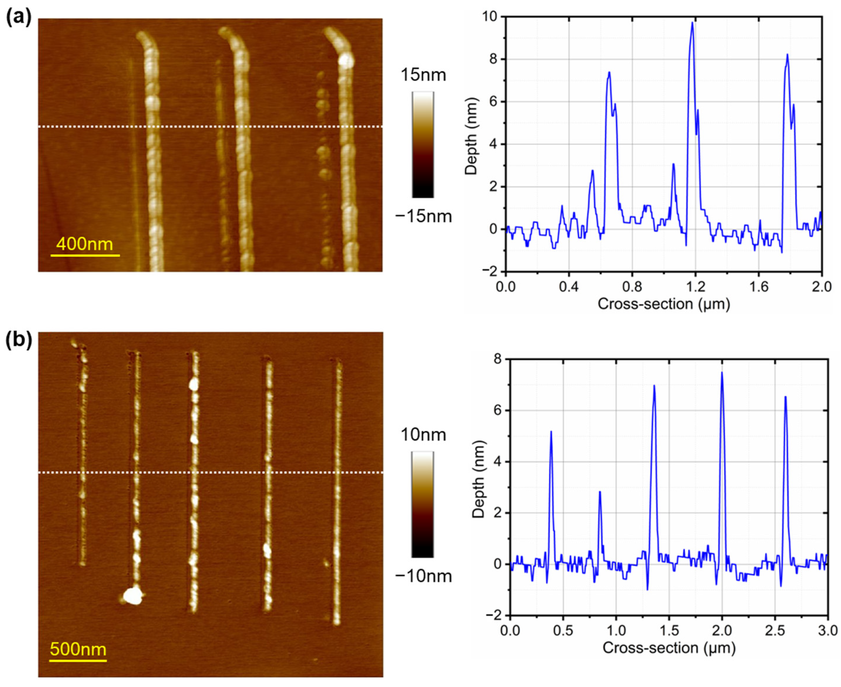
3.2. Comparation between Nano-Scratching and Dynamic Lithography
3.3. Characterization on Nanofabrication Quality of Dynamic Lithography
4. Conclusions
Author Contributions
Funding
Data Availability Statement
Conflicts of Interest
References
- Radisavljevic, B.; Radenovic, A.; Brivio, J.; Giacometti, V.; Kis, A. Single-layer MoS2 transistors. Nat. Nanotechnol. 2011, 6, 147–150. [Google Scholar] [CrossRef] [PubMed]
- Hu, Z.; Wu, Z.; Han, C.; He, J.; Ni, Z.; Chen, W. Two-dimensional transition metal dichalcogenides: Interface and defect engineering. Chem. Soc. Rev. 2018, 47, 3100–3128. [Google Scholar] [CrossRef] [PubMed]
- Fathi-Hafshejani, P.; Azam, N.; Wang, L.; Kuroda, M.A.; Hamilton, M.C.; Hasim, S.; Mahjouri-Samani, M. Two-dimensional-material-based field-effect transistor biosensor for detecting COVID-19 Virus (SARS-CoV-2). ACS Nano 2021, 15, 11461–11469. [Google Scholar] [CrossRef]
- Park, H.; Park, J.; Kang, S.; Jeong, S. 3D-nanostructured MoS2 nanoscroll with highly active sites for improving NO2 gas detection. Mater. Lett. 2023, 349, 134733. [Google Scholar] [CrossRef]
- Liang, J.; Xu, K.; Toncini, B.; Bersch, B.; Jariwala, B.; Lin, Y.; Robinson, J.; Fullerton-Shirey, S.K. Impact of post-lithography polymer residue on the electrical characteristics of MoS2 and WSe2 field effect transistors. Adv. Mater. Interfaces 2019, 6, 1801321. [Google Scholar] [CrossRef]
- Jia, Y.; Gong, X.; Peng, P.; Wang, Z.; Tian, Z.; Ren, L.; Fu, Y.; Zhang, H. Toward high carrier mobility and low contact resistance: Laser cleaning of PMMA residues on graphene surfaces. Nano-Micro Lett. 2016, 8, 336–346. [Google Scholar] [CrossRef] [PubMed]
- Suk, J.W.; Lee, W.H.; Lee, J.; Chou, H.; Piner, R.D.; Hao, Y.; Akinwande, D.; Ruoff, R.S. Enhancement of the electrical properties of graphene grown by chemical vapor deposition via controlling the effects of polymer residue. Nano Lett. 2013, 13, 1462–1467. [Google Scholar] [CrossRef] [PubMed]
- Choi, J.; Zhang, H.; Du, H.; Choi, J.H. Understanding solvent effects on the properties of two-dimensional transition metal dichalcogenides. ACS Appl. Mater. Interfaces 2016, 8, 8864–8869. [Google Scholar] [CrossRef]
- Thoutam, L.R.; Mathew, R.; Ajayan, J.; Tayal, S.; Nair, S.V. A critical review of fabrication challenges and reliability issues in top/bottom gated MoS2 field-effect transistors. Nanotechnology 2023, 34, 232001. [Google Scholar] [CrossRef]
- Tilmann, R.; Bartlam, C.; Hartwig, O.; Tywoniuk, B.; Dominik, N.; Cullen, C.P.; Peters, L.; Stimpel-Lindner, T.; McEvoy, N.; Duesberg, G.S. Identification of ubiquitously present polymeric adlayers on 2D transition metal dichalcogenides. ACS Nano 2023, 17, 10617–10627. [Google Scholar] [CrossRef]
- Chang, S.; Yan, Y.; Geng, Y. Local nanostrain engineering of monolayer MoS2 using atomic force microscopy-based thermomechanical nanoindentation. Nano Lett. 2023, 23, 9219–9226. [Google Scholar] [CrossRef] [PubMed]
- Zheng, X.; Calò, A.; Albisetti, E.; Liu, X.; Alharbi, A.S.M.; Arefe, G.; Liu, X.; Spieser, M.; Yoo, W.J.; Taniguchi, T.; et al. Patterning metal contacts on monolayer MoS2 with vanishing Schottky barriers using thermal nanolithography. Nat. Electron. 2019, 2, 17–25. [Google Scholar] [CrossRef]
- Dago, A.I.; Ryu, Y.K.; Palomares, F.J.; Garcia, R. Direct patterning of p-type-doped few-layer WSe2 nanoelectronic devices by oxidation scanning probe lithography. ACS Appl. Mater. Interfaces 2018, 10, 40054–40061. [Google Scholar] [CrossRef] [PubMed]
- Li, J.; Yi, S.; Wang, K.; Liu, Y.; Li, J. Alkene-catalyzed rapid layer-by-layer thinning of black phosphorus for precise nanomanufacturing. ACS Nano 2022, 16, 13111–13122. [Google Scholar] [CrossRef] [PubMed]
- Rani, E.; Wong, L.S. High-resolution scanning probe nanolithography of 2D materials: Novel nanostructures. Adv. Mater. Technol. 2019, 4, 1900181. [Google Scholar] [CrossRef]
- Khac, B.T.; DelRio, F.W.; Chung, K. Interfacial strength and surface damage characteristics of atomically thin h-BN, MoS2, and graphene. ACS Appl. Mater. Interfaces 2018, 10, 9164–9177. [Google Scholar] [CrossRef] [PubMed]
- Ye, S.; Xu, K.; Lei, L.; Hussain, S.; Pang, F.; Liu, X.; Zheng, Z.; Ji, W.; Shi, X.; Xu, R.; et al. Nanoscratch on single-layer MoS2 crystal by atomic force microscopy: Semi-circular to periodical zigzag cracks. Mater. Res. Express 2019, 6, 025048. [Google Scholar] [CrossRef]
- Zhang, Y.; Liu, J.; Pan, Y.; Luo, K.; Yu, J.; Zhang, Y.; Jia, K.; Yin, H.; Zhu, H.; Tian, H.; et al. The evolution of MoS2 properties under oxygen plasma treatment and its application in MoS2 based devices. J. Mater. Sci. Mater. Electron. 2019, 30, 18185–18190. [Google Scholar] [CrossRef]
- Pei, C.; Li, X.; Fan, H.; Wang, J.; You, H.; Yang, P.; Wei, C.; Wang, S.; Shen, X.; Li, H. Morphological and spectroscopic characterizations of monolayer and few-layer MoS2 and WSe2 nanosheets under oxygen plasma treatment with different excitation power: Implications for modulating electronic properties. ACS Appl. Nano Mater. 2020, 3, 4218–4230. [Google Scholar] [CrossRef]
- Ryu, Y.K.; Dago, A.I.; He, Y.; Espinosa, F.M.; Lopez-Elvira, E.; Munuera, C.; Garcia, R. Sub-10 nm patterning of few-layer MoS2 and MoSe2 nanolectronic devices by oxidation scanning probe lithography. Appl. Surf. Sci. 2021, 539, 148231. [Google Scholar] [CrossRef]
- Vasić, B.; Kratzer, M.; Matković, A.; Nevosad, A.; Ralević, U.; Jovanović, D.; Ganser, C.; Teichert, C.; Gajić, R. Atomic force microscopy based manipulation of graphene using dynamic plowing lithography. Nanotechnology 2013, 24, 015303. [Google Scholar] [CrossRef]
- Vasić, B.; Matković, A.; Gajić, R. Phase imaging and nanoscale energy dissipation of supported graphene using amplitude modulation atomic force microscopy. Nanotechnology 2017, 28, 465708. [Google Scholar] [CrossRef]


| Vw/Vr | Unmachined Surface Ra (nm) | Machined Surface Ra (nm) |
|---|---|---|
| 10 | 0.13 | 0.17 |
| 15 | 0.20 | 0.31 |
| 20 | 0.19 | 0.21 |
Disclaimer/Publisher’s Note: The statements, opinions and data contained in all publications are solely those of the individual author(s) and contributor(s) and not of MDPI and/or the editor(s). MDPI and/or the editor(s) disclaim responsibility for any injury to people or property resulting from any ideas, methods, instructions or products referred to in the content. |
© 2024 by the authors. Licensee MDPI, Basel, Switzerland. This article is an open access article distributed under the terms and conditions of the Creative Commons Attribution (CC BY) license (https://creativecommons.org/licenses/by/4.0/).
Share and Cite
He, Y.; Su, X.; Hai, K. Machinability of MoS2 after Oxygen Plasma Treatment under Mechanical Scanning Probe Lithography. Crystals 2024, 14, 280. https://doi.org/10.3390/cryst14030280
He Y, Su X, Hai K. Machinability of MoS2 after Oxygen Plasma Treatment under Mechanical Scanning Probe Lithography. Crystals. 2024; 14(3):280. https://doi.org/10.3390/cryst14030280
Chicago/Turabian StyleHe, Yang, Xing Su, and Kuo Hai. 2024. "Machinability of MoS2 after Oxygen Plasma Treatment under Mechanical Scanning Probe Lithography" Crystals 14, no. 3: 280. https://doi.org/10.3390/cryst14030280
APA StyleHe, Y., Su, X., & Hai, K. (2024). Machinability of MoS2 after Oxygen Plasma Treatment under Mechanical Scanning Probe Lithography. Crystals, 14(3), 280. https://doi.org/10.3390/cryst14030280