
Ultrathin Encapsulation Strategies with Predefined Gate Dielectric Surface Area for Flexible Crystalline Silicon Nanomembrane-Based MOS Capacitors

Abstract
1. Introduction
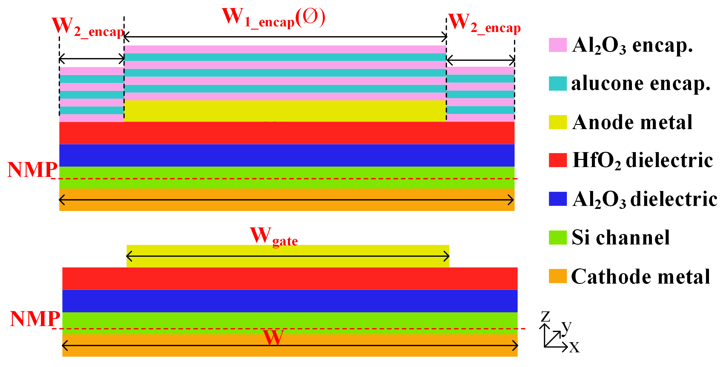
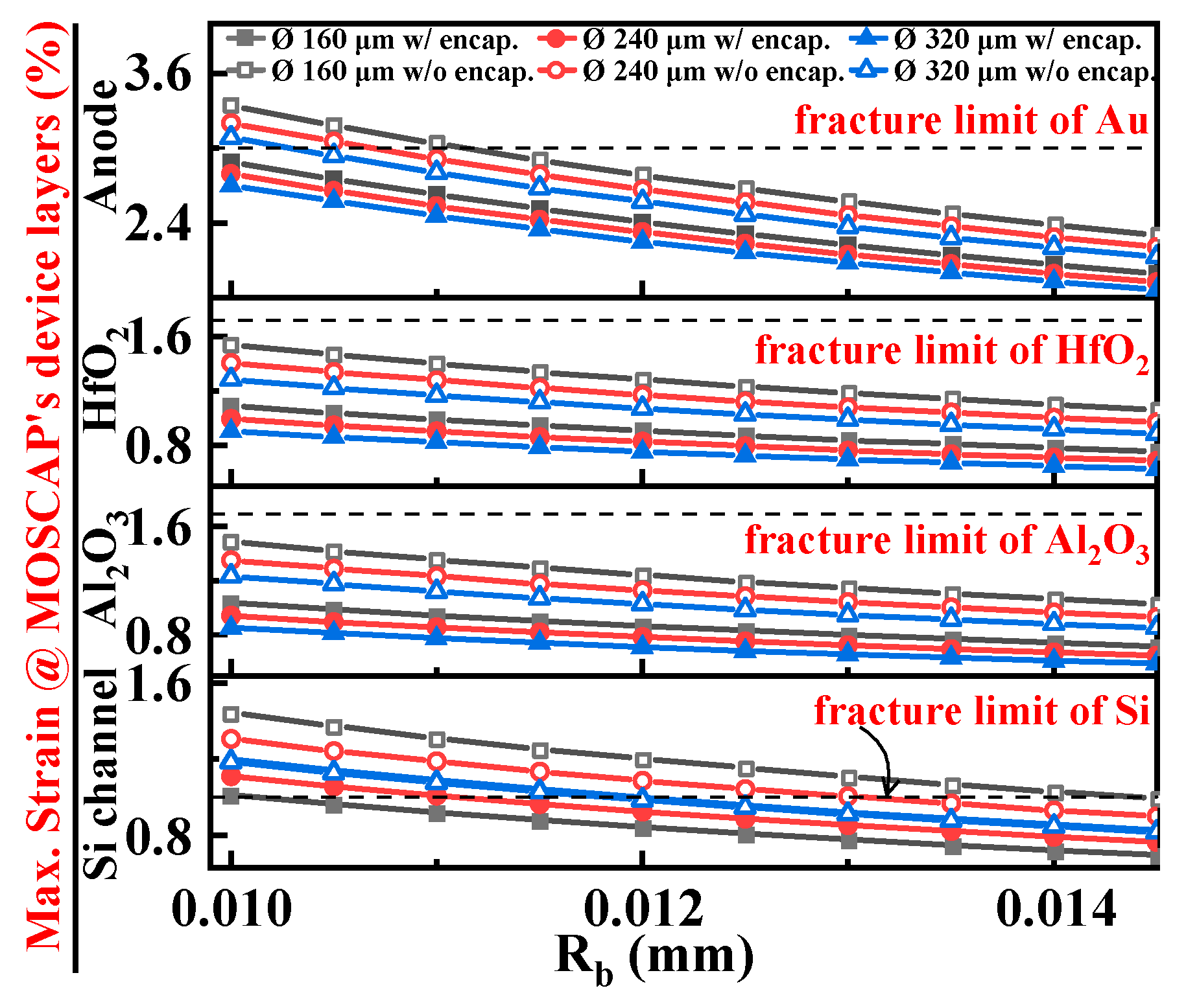
2. Maximum Strain Analysis in the Device Layer for Al2O3/Alucone-Encapsulated and Bare MOSCAPs with Different Ø
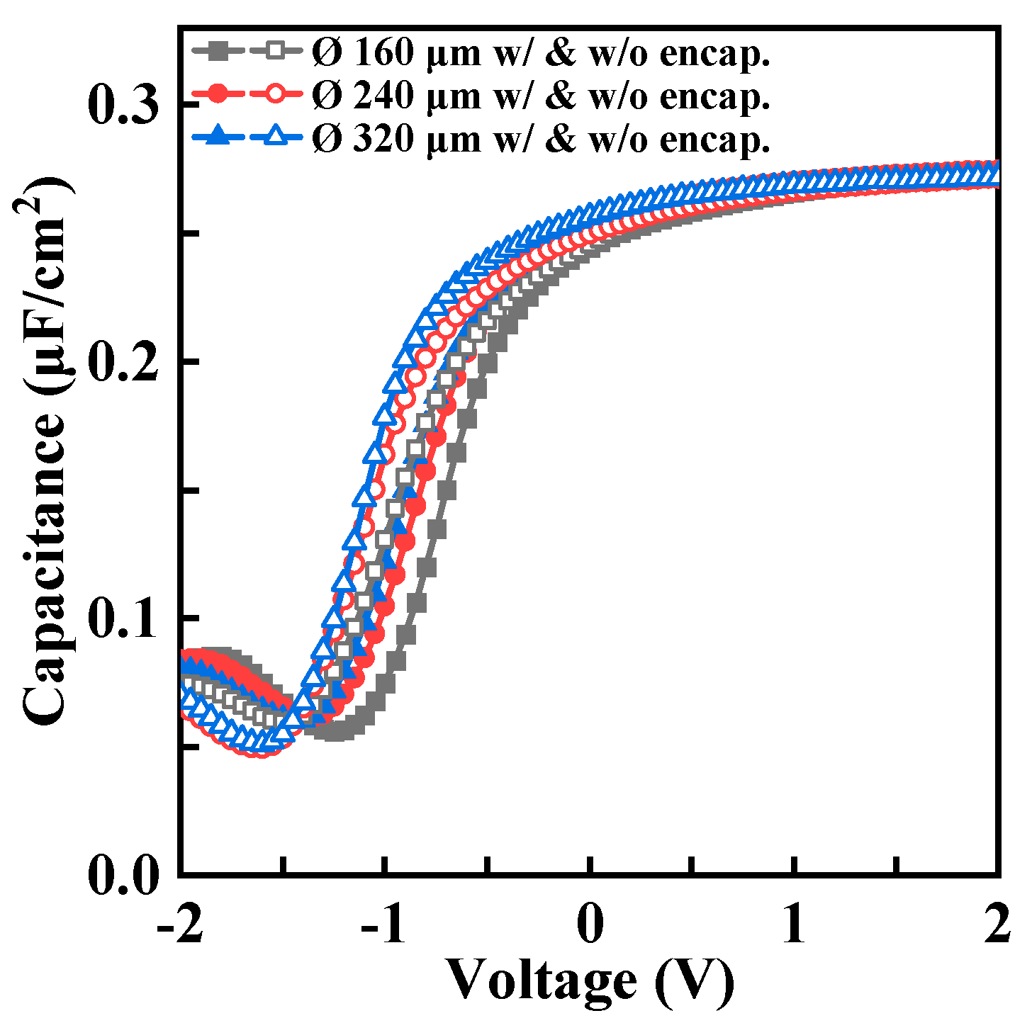
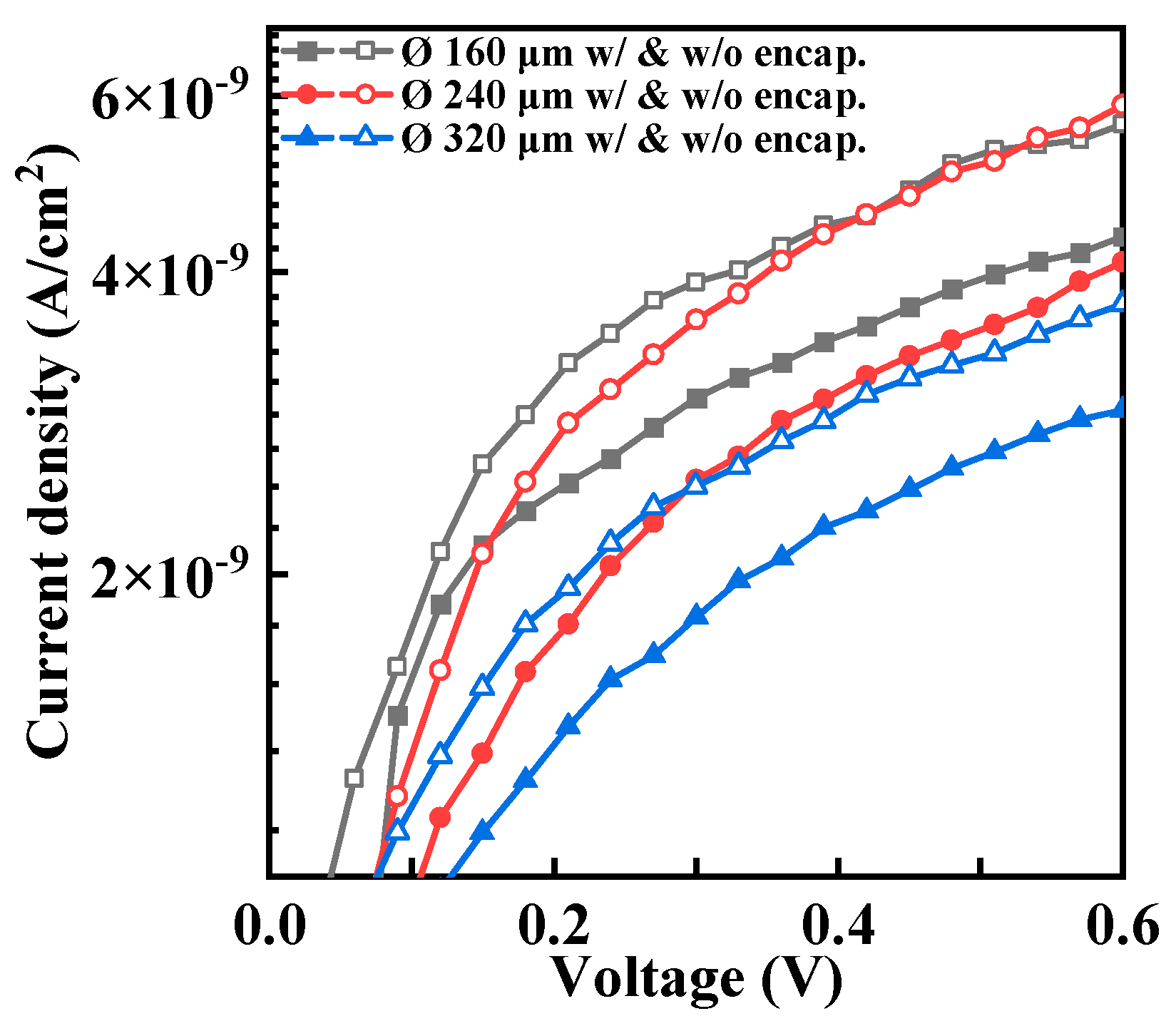
3. C-V and J-V Characteristics in the Planar State for Encapsulated and Bare MOSCAPs with Different Ø
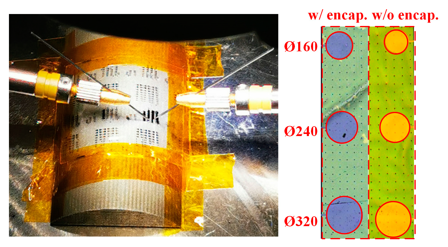
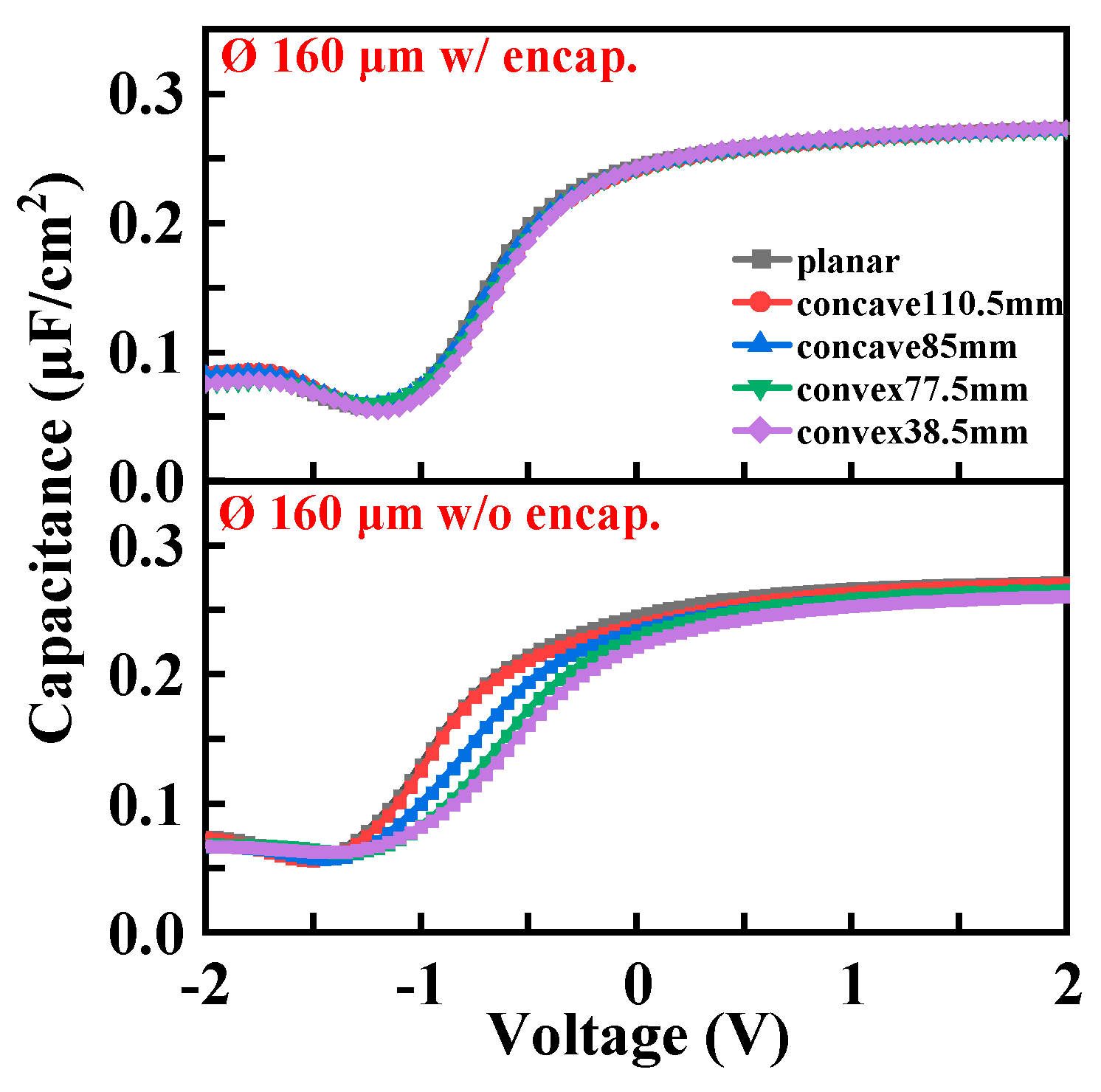
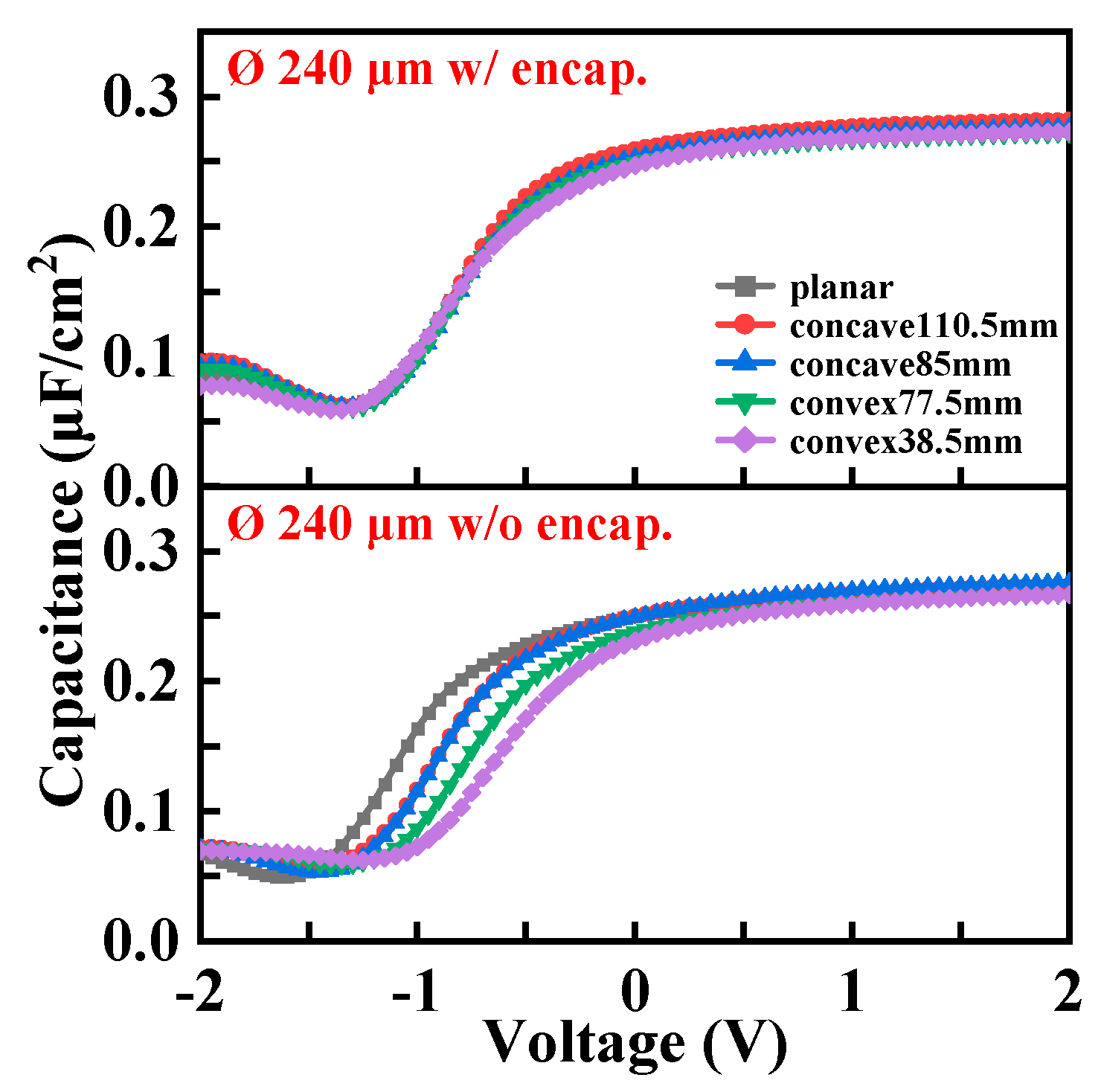
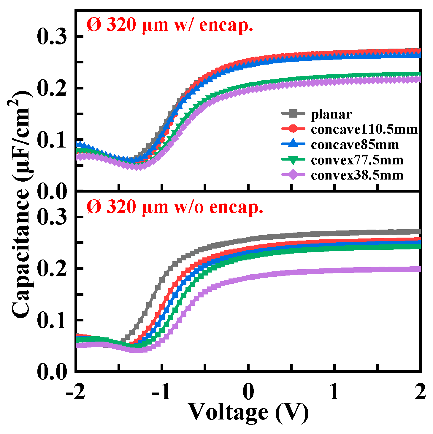
4. Electro-Mechanical Analysis under Bending Conditions for Encapsulated and Bare MOSCAPs with Different Ø
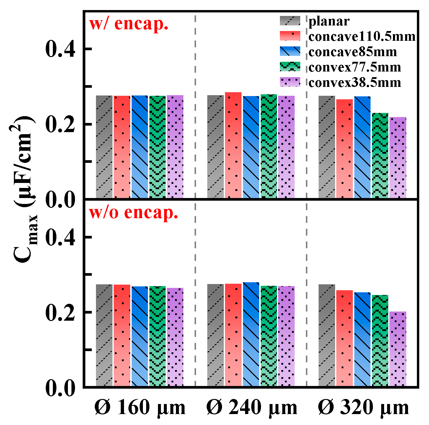
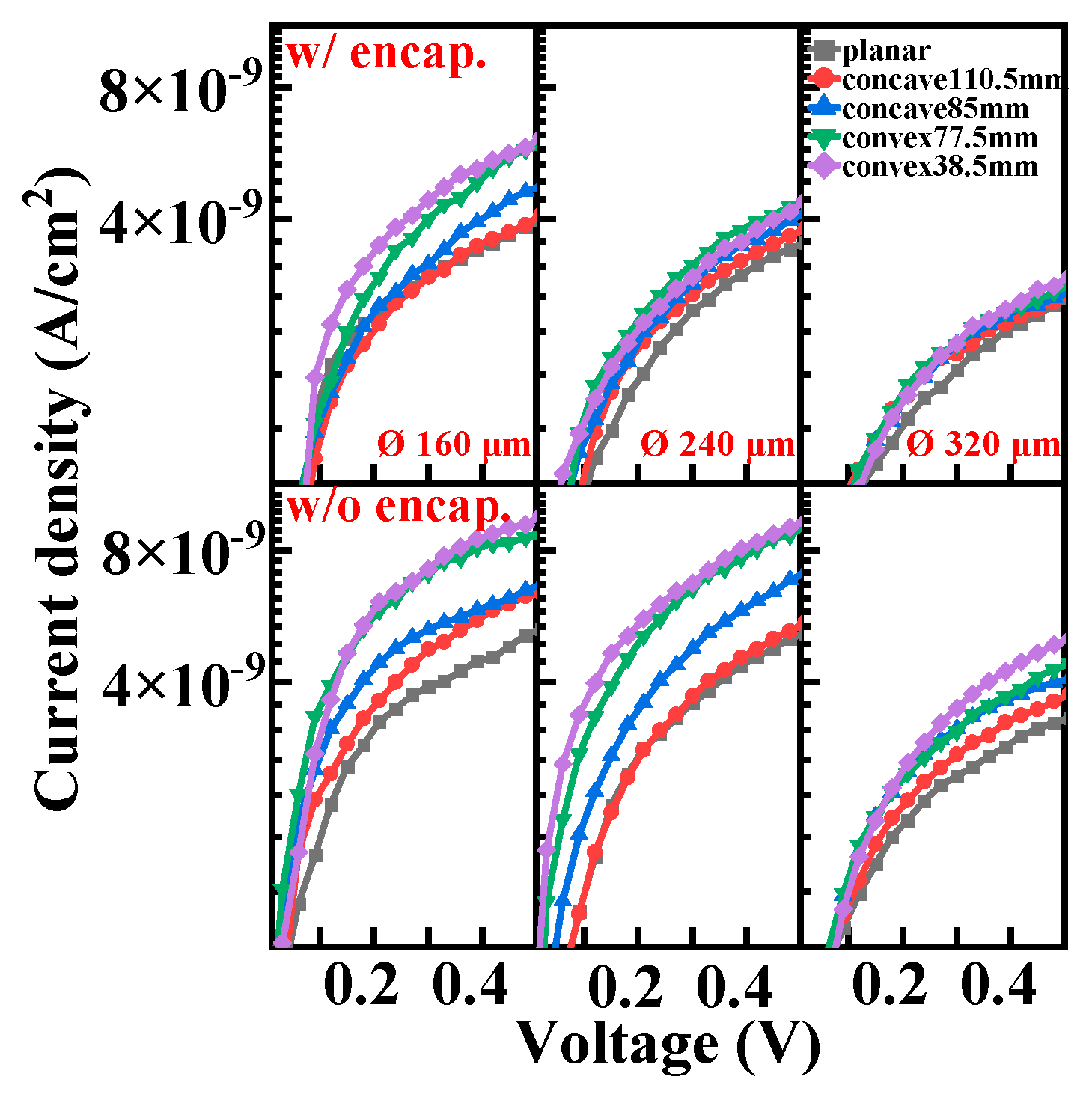
4.1. Comparative Analysis on Basic Electrical Properties
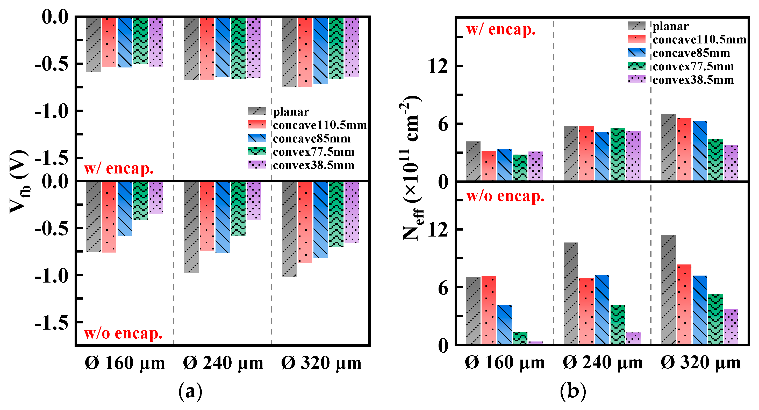
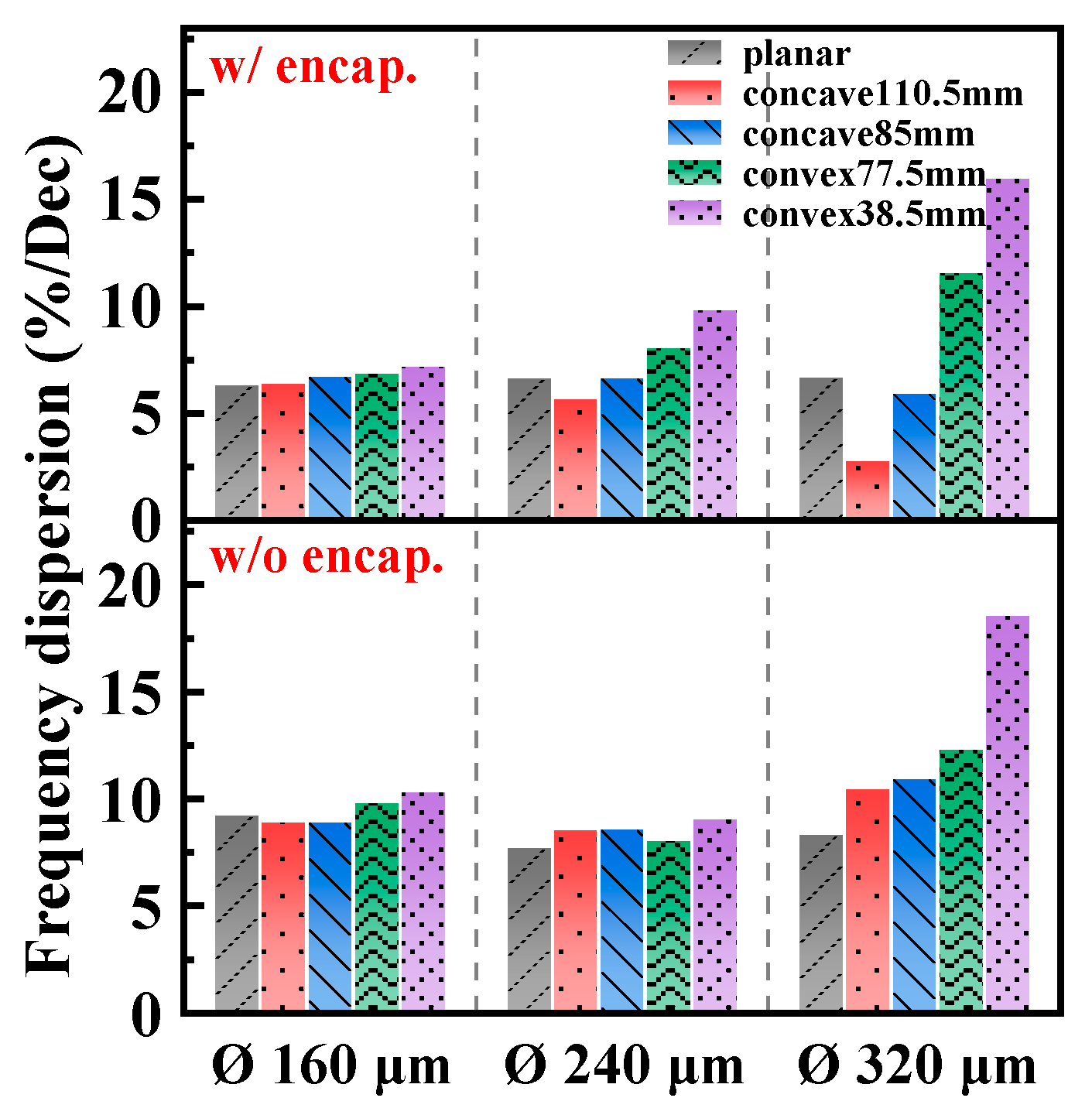
4.2. Comparative Analysis of Extracted Parameters
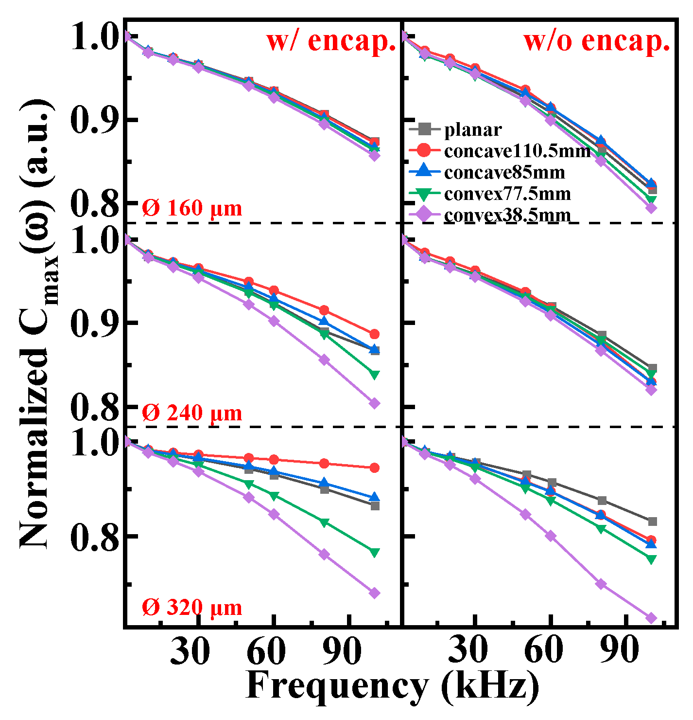
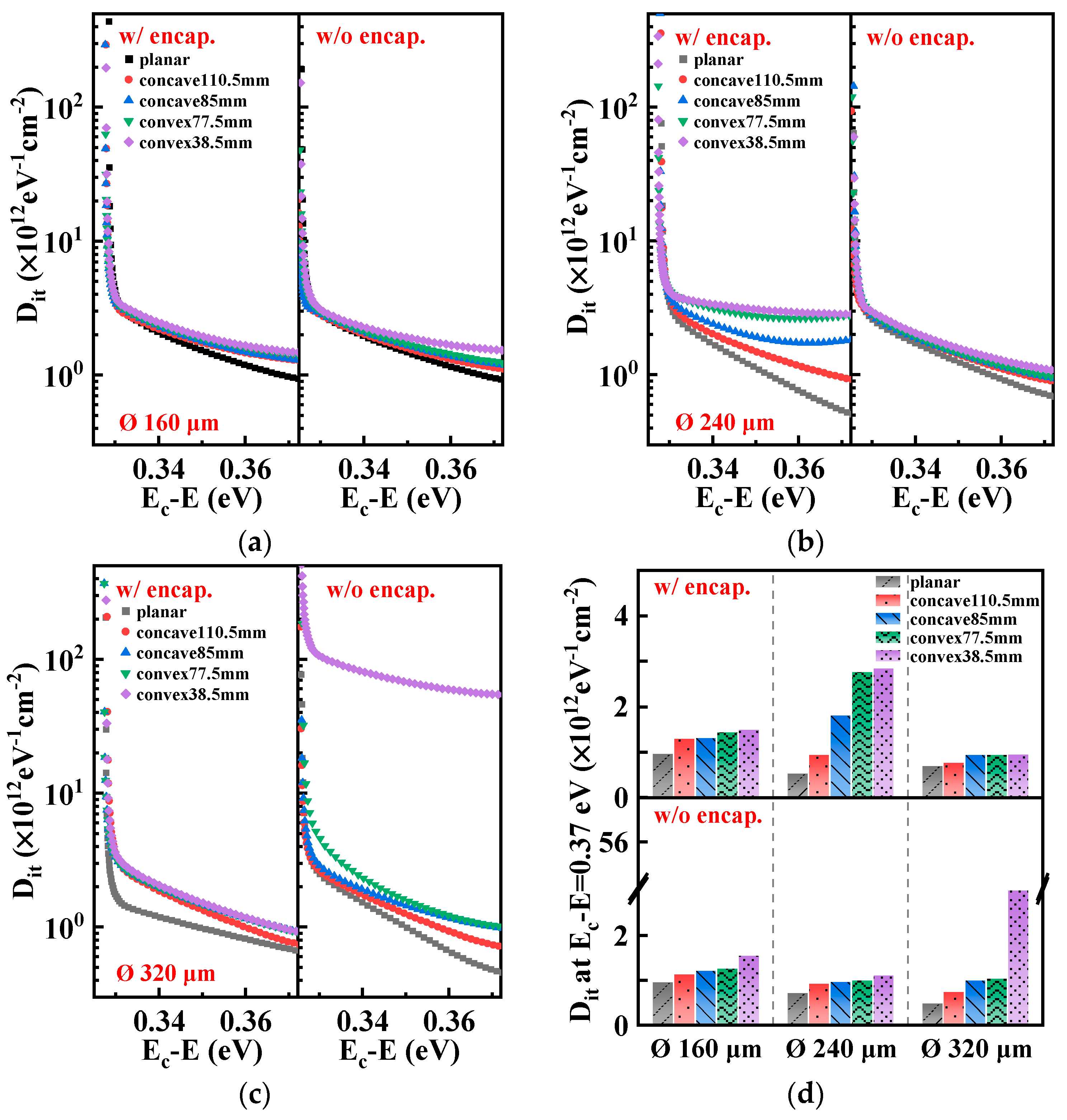
4.3. Comparative Analysis on Interfacial Characteristics
5. Conclusions
Author Contributions
Funding
Data Availability Statement
Conflicts of Interest
Appendix A
References
- Mariello, M.; Kim, K.; Wu, K.; Lacour, S.P.; Leterrier, Y. Recent advances in encapsulation of flexible bioelectronic implants: Materials, technologies, and characterization methods. Adv. Mater. 2022, 34, 2201129. [Google Scholar] [CrossRef]
- Cho, Y.; Park, S.; Lee, J.; Yu, K.J. Emerging materials and technologies with applications in flexible neural implants: A comprehensive review of current issues with neural devices. Adv. Mater. 2021, 33, 2005786. [Google Scholar] [CrossRef] [PubMed]
- Oldroyd, P.; Malliaras, G.G. Achieving long-term stability of thin-film electrodes for neurostimulation. Acta Biomater. 2022, 139, 65–81. [Google Scholar] [CrossRef]
- Sinha, S.; Pal, T. A comprehensive review of FET-based pH sensors: Materials, fabrication technologies, and modeling. Electrochem. Sci. Adv. 2022, 2, e2100147. [Google Scholar] [CrossRef]
- Khau, B.V.; Scholz, A.D.; Reichmanis, E. Advances and opportunities in development of deformable organic electrochemical transistors. J. Mater. Chem. C 2020, 8, 15067–15078. [Google Scholar] [CrossRef]
- Lee, J.Y.; Shin, J.; Kim, K.; Ju, J.E.; Dutta, A.; Kim, T.S.; Cho, Y.U.; Kim, T.; Hu, L.; Min, W.K.; et al. Ultrathin crystalline silicon nano and micro membranes with high areal density for low-cost flexible electronics. Small 2023, 19, 2302597. [Google Scholar] [CrossRef] [PubMed]
- Seo, K.J.; Hill, M.; Ryu, J.; Chiang, C.H.; Rachinskiy, I.; Qiang, Y.; Jang, D.; Trumpis, M.; Wang, C.; Viventi, J.; et al. A soft, high-density neuroelectronic array. npj Flex. Electron. 2023, 7, 40. [Google Scholar] [CrossRef]
- Multia, J.; Karppinen, M. Atomic/Molecular layer deposition for designer’s functional metal–organic materials. Adv. Mater. Interfaces 2022, 9, 2200210. [Google Scholar] [CrossRef]
- Niemelä, J.P.; Rohbeck, N.; Michler, J.; Utke, I. Molecular layer deposited alucone thin films from long-chain organic precursors: From brittle to ductile mechanical characteristics. Dalton Trans. 2020, 49, 10832–10838. [Google Scholar] [CrossRef]
- Xiao, W.; Hui, D.Y.; Zheng, C.; Yu, D.; Qiang, Y.Y.; Ping, C.; Xiang, C.L.; Yi, Z. A flexible transparent gas barrier film employing the method of mixing ALD/MLD-grown Al2O3 and alucone layers. Nanoscale Res. Lett. 2015, 10, 130. [Google Scholar] [CrossRef]
- Kim, L.H.; Jang, J.H.; Jeong, Y.J.; Kim, K.; Baek, Y.; Kwon, H.J.; An, T.K.; Nam, S.; Kim, S.H.; Jang, J.; et al. Highly-impermeable Al2O3/HfO2 moisture barrier films grown by low-temperature plasma-enhanced atomic layer deposition. Org. Electron. 2017, 50, 296–303. [Google Scholar] [CrossRef]
- Cao, K.; Chen, R.; Li, Y.; Xiong, Y.; Yang, H. Thin film encapsulation for the organic light-emitting diodes display via atomic layer deposition. J. Mater. Res. 2020, 35, 681–700. [Google Scholar]
- Fang, H.; Yu, K.J.; Gloschat, C.; Yang, Z.; Song, E.; Chiang, C.H.; Zhao, J.; Won, S.M.; Xu, S.; Trumpis, M.; et al. Capacitively coupled arrays of multiplexed flexible silicon transistors for long-term cardiac electrophysiology. Nat. Biomed. Eng. 2017, 1, 0038. [Google Scholar]
- Bao, M. Analysis and Design Principles of MEMS Devices, 1st ed; Elsevier Science: Amsterdam, The Netherlands, 2005; pp. 54–59. [Google Scholar]
- Liu, C.; Wang, Z.; Zhang, Y.; Lü, H.; Zhang, Y.M. Nanolaminated HfO2/Al2O3 dielectrics for high-performance silicon nanomembrane based field-effect transistors on biodegradable substrates. Adv. Mater. Interfaces 2022, 9, 2201477. [Google Scholar] [CrossRef]
- Liu, C.; Zhang, Y.; Zhang, Y.M.; Lü, H.L. Interfacial characteristics of Al/Al2O3/ZnO/n-GaAs MOS capacitor. Chin. Phys. B 2013, 22, 076701. [Google Scholar] [CrossRef]
- Cao, Y.; Allameh, S.; Nankivil, D.; Sethiaraj, S.; Otiti, T.; Soboyejo, W. Nanoindentation measurements of the mechanical properties of polycrystalline Au and Ag thin films on silicon substrates: Effects of grain size and film thickness. Mater. Sci. Eng. A 2006, 427, 232–240. [Google Scholar] [CrossRef]
- Park, S.I.; Ahn, J.H.; Feng, X.; Wang, S.; Huang, Y.; Rogers, J.A. Theoretical and experimental studies of bending of inorganic electronic materials on plastic substrates. Adv. Funct. Mater. 2008, 18, 2673–2684. [Google Scholar] [CrossRef]
- Chang, H.Y.; Yang, S.; Lee, J.; Tao, L.; Hwang, W.S.; Jena, D.; Lu, N.; Akinwande, D. High-performance, highly bendable MoS2 transistors with high-k dielectrics for flexible low-power systems. ACS Nano 2013, 7, 5446–5452. [Google Scholar] [CrossRef]
- Rontu, V.; Nolvi, A.; Hokkanen, A.; Haeggström, E.; Kassamakov, I.; Franssila, S. Elastic and fracture properties of free-standing amorphous ALD Al2O3 thin films measured with bulge test. Mater. Res. Express 2018, 5, 046411. [Google Scholar] [CrossRef]
- Berdova, M.; Liu, X.; Wiemer, C.; Lamperti, A.; Tallarida, G.; Cianci, E.; Fanciulli, M.; Franssila, S. Hardness, elastic modulus, and wear resistance of hafnium oxide-based films grown by atomic layer deposition. J. Vac. Sci. Technol. A 2016, 34, 051510. [Google Scholar] [CrossRef]
- Ruoho, M.; Tarasiuk, N.; Rohbeck, N.; Kapusta, C.; Michler, J.; Utke, I. Stability of mechanical properties of molecular layer–deposited alucone. Mater. Today Chem. 2018, 10, 187–194. [Google Scholar] [CrossRef]

Disclaimer/Publisher’s Note: The statements, opinions and data contained in all publications are solely those of the individual author(s) and contributor(s) and not of MDPI and/or the editor(s). MDPI and/or the editor(s) disclaim responsibility for any injury to people or property resulting from any ideas, methods, instructions or products referred to in the content. |
© 2024 by the authors. Licensee MDPI, Basel, Switzerland. This article is an open access article distributed under the terms and conditions of the Creative Commons Attribution (CC BY) license (https://creativecommons.org/licenses/by/4.0/).
Share and Cite
Wang, Z.; Lu, H.; Zhang, Y.; Liu, C. Ultrathin Encapsulation Strategies with Predefined Gate Dielectric Surface Area for Flexible Crystalline Silicon Nanomembrane-Based MOS Capacitors. Crystals 2024, 14, 190. https://doi.org/10.3390/cryst14020190
Wang Z, Lu H, Zhang Y, Liu C. Ultrathin Encapsulation Strategies with Predefined Gate Dielectric Surface Area for Flexible Crystalline Silicon Nanomembrane-Based MOS Capacitors. Crystals. 2024; 14(2):190. https://doi.org/10.3390/cryst14020190
Chicago/Turabian StyleWang, Zhuofan, Hongliang Lu, Yuming Zhang, and Chen Liu. 2024. "Ultrathin Encapsulation Strategies with Predefined Gate Dielectric Surface Area for Flexible Crystalline Silicon Nanomembrane-Based MOS Capacitors" Crystals 14, no. 2: 190. https://doi.org/10.3390/cryst14020190
APA StyleWang, Z., Lu, H., Zhang, Y., & Liu, C. (2024). Ultrathin Encapsulation Strategies with Predefined Gate Dielectric Surface Area for Flexible Crystalline Silicon Nanomembrane-Based MOS Capacitors. Crystals, 14(2), 190. https://doi.org/10.3390/cryst14020190